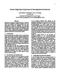
Model-based Exploration of the Design Space for Heterogeneous Systems on Chip H. Blume, H. Hübert, H. T. Feldkämper, T. G. Noll Chair of Electrical Engineering and Computer Systems Institute of Technology, RWTH Aachen Schinkelstr. 2, 52062 Aachen, GERMANY
[email protected] Abstract The exploration of the design space for heterogeneous reconfigurable Systems on Chip (SoC) becomes more and more important. As modern SoCs include a variety of different architecture blocks ensuring flexibility as well as highest performance, it is mandatory to prune the design space in an early stage of the design process in order to achieve short innovation cycles for new products. Therefore, the goal of this work is to provide estimations of implementation specif ic parameters like throughput rate, power dissipation and silicon area by means of cost functions. A concept for a model based exploration strategy supporting the design flow for heterogeneous SoCs is presented. In order to prove the feasibility of this exploration strategy first of all operations were implemented on discrete components like DSPs, FPGAs or dedicated ASICs. Implementation parameters are provided for a variety of basic operations frequently required in digital signal processing. These implementation parameters serve as a basis for deriving models for the design space exploration concept.
1. Introduction For today's high-performance and computational intensive systems for e.g. video processing or wireless communication a high degree of flexibility and highest computational capacities have to be provided. But the computational demands are well beyond the performance of today's programmable processor based platforms [5], [12]. For example in [8] the increase in computational demands evolving from one communication standard to the next one has been compared to the increase in performance of digital signal processor (DSP) kernels. It is shown that the computational requirements stay well beyond the available performance of on-chip DSP kernels (Figure 1). Even more severe, future gene rations of communication standards strengthen this computational gap. In addition to these computational demands different forms of required flexibility have to be distinguished: • short innovation cycles e.g. in the consumer electronic field demand for possibilities to integrate new features from one product generation to the next one, respectively enforce to integrate new algorithmic updates to increase the system quality • adaptation to standard updates (e.g. variation of chiprate with evolution of a communication standard like UMTS), causing redesign time and effort and resulting typically in increased time-to-market • runtime adaptation due to switching between several cells/standards (e.g. handover between GPRS/EDGE/UMTS), respectively adaptation to channel quality Therefore, the underlying architecture of many electronic products has to include architecture blocks that provide sufficient flexibility to match the requirements. Generally, dedicated hardware implementations offer orders of magnitude better performance with respect to throughput and power dissipation. But flexibility of those implementations is restricted to weak programmability (e.g. switching coefficients) considered at design time.
MIPS
required
5000
computational performance
2000
available
1000
computational performance
500
100
GSM
expected 600 MHz 4800 MIPS
300 MHz 1200 MIPS
160 MHz 320 MIPS
90 MHz 90 MIPS
50 20
UMTS
EDGE
GPRS
200
? +adaptive -antenna - coding
30 MHz 30 MIPS
10 ‘97
‘98
‘99
‘00
‘01
‘02
‘03
Year
Figure 1. Increase in computational complexity and available DSP-performance [8] A qualitative comparison of flexibility, performance and power consumption among today's available building block implementation styles is depicted in Figure 2. Altogether, a wellbalanced architecture of a sophisticated, high performance SoC has to include different types of architecture blocks in order to provide the required performance at reasonable costs (area, power dissipation, throughput rate) on one hand and ensuring sufficient flexibility on the other. Digital Signal Processor Core
10 2 W Application Specific Signal Processor Core
Embedded FPGA Standard Cell Macro Physically Optimized Macro
10-3 h-1
10 -3 W 102 MOPS
Log
PERFORMANCE
Log P O W E R D I S S I P A T I O N
General Purpose Processor Core
Log F L E X I B I L I T Y
1 h-1
106 MOPS
Figure 2. Trade-off between flexibility, performance and power consumption Therefore, according to the required performance and flexibility systems have to be partitioned into system blocks, which have to be mapped to appropriate architecture blocks (see Figure 3). In order to meet the challenging demands of such a partitioning and mapping process it is important to elaborate strategies, models and tool methodologies which assist designers with metrics and with an early assessment of the capabilities of a given platform [3], [12]. In order to achieve competitive results implementing a SoC, it is required to explore the available design space in an early phase of the design process. This paper is organized as follows: In chapter 2 the problems connected to the design flow for heterogeneous architectures is reviewed and possible solution strategies are worked out. The concept of a model based partitioning strategy for design space exploration is presented. In chapter 3 the different architecture blocks are described. In chapter 4 optimizations for the
architecture blocks and the results for frequently used basic operations are discussed. Chapter 5 shows an example for the partitioning and mapping of a system onto a heterogeneous architecture. Conclusions are given in chapter 6. coprocessor 1 copro- FPGA cessor 2
system filter system blocks
image analysis module
motion estimation
DSP core
...
coprocessor x
on-chip memory
System-on-Chip
architecture blocks µC
partitioning and mapping
Figure 3. Partitioning and mapping of a system to a heterogeneous architecture
2. Design Flow for Heterogeneous Architectures 2.1. Problems related to conventional design flows A very simplified conventional design flow for heterogeneous architectures is depicted in Figure 4. system design simulation of algorithms
time consuming feedback
ASIC/SW design partitioning RTL/C code
physical design mask layout
Figure 4. Conventional design flow for heterogeneous architectures [5] Different design levels such as system, architecture and physical level are shown. The typical, undesirable time consuming feedback loops arise as often the specification can not been met with the first approach. This results in the following alternatives at system level: • The initial partitioning/mapping of the algorithm to the heterogeneous architecture has to be altered. One possibility is to distribute the system blocks on the architecture blocks in a different way, e.g. implementing the critical block no longer on the given DSP core but selecting another one or implementing it in dedicated hardware. This will be a time consuming process as it requires a new design for at least some system blocks. Therefore, this feedback from architecture to system level prolongates the innovation cycles. • The other possibility is to restrict the parameters of the design (e.g. restriction of algorithmic parameters like the size of the search area of blockmatching) as a consequence of
the feedback from architecture level. This results in a loss of system quality for the sake of reduced redesign effort. Here, system quality is traded for design time. Even worse, the more heterogeneous future SoCs will be, the more complex this design space exploration will be. In order to solve this problem several approaches have been proposed in the literature. For example in [5], a methodology for a hierarchical automated design flow is presented, that generates from an initial description on system level a direct mapped architecture. In [14] an extensible simulation integration framework is presented. This framework supports multi-granular simulation of embedded systems by integrating (e.g. power/ performance) simulators into a unified environment. By this, a design space exploration and pruning of the design space is performed. Starting with initial design descriptions interpreters translate these into the input of the selected simulators. These simulation results need to be incorporated back in the design description. This methodology highly depends on the interfacing between several simulators and translators. Hence, the number of addressable architecture blocks is significantly limited by the number and efficiency of integrated simulators. And even worse for some simulators this feedback of simulation results will necessarily be a "human-in-the-loop process". A methodology called SPADE is presented in [15]. This methodology allows to explore the design space for heterogeneous architectures. SPADE distinguishes between application and architecture models. It uses a trace-driven simulation technique for co-simulation. This tool yields performance metrics for architecture blocks out of a library of generic building blocks e.g. in form of processor utilization or the number of read/write stalls on the I/O ports. All of these approaches try to integrate several design tools (e.g. for synthesis or co-simulation) into the design flow. Hence, the extent of the design space exploration is limited by the time effort for deriving fairly accurate values by passing the complete tool chain. And even worse, the interfacing between the tools is not always automated. This significantly restricts the number of possible feedbacks. Furthermore, the variety of design alternatives is restricted to those alternatives which are supported by the integrated tools. But for some alternatives (e.g. high performance macros) no pure tool based generation is possible. For example even in standard cell design the trend to integrate hand optimized standard cells in order to achieve highest performance becomes important [11]. Relying solely on pure tool based concepts means not to pay regard to the complete degree of heterogeneity respectively performance demands. Opposed to these concepts we propose a methodology applying parameterized feature models for system functions covering the complete variety of architecture blocks and helping to better explore the heterogeneous design space. 2.2. A model based partitioning strategy for efficient design space exploration As was shown, in an early stage of the design process of a SoC a design space exploration is required. It should be possible to evaluate different partitioning/mapping alternatives concerning important characteristic features like resulting power dissipation, silicon area, CPU usage of processor cores, throughput rate etc. Only the system designer will be able to partition the system in that sense that the required flexibility is kept. But in order to avoid time consuming feedbacks between several design levels a deeper hardware/architecture knowledge is required even on system level. Therefore, a model based partitioning concept is proposed here being depicted in Figure 5. A cost evaluation tool supports the system designer by allowing an exploration of the design space. This tool requires information about the system specification (e.g. symbol rate, filter parameters etc.). Furthermore, a system partitioning and a mapping to specific architecture blocks can be passed over to this tool. An additional input is the access to a model library. This library includes parameterized models of the characteristic features (silicon area, power consumption,
throughput rate) for the functional blocks of the chosen application domain (e.g. models for digital filter architectures, Viterbi decoders, Reed Solomon decoders).
system design
partitioning/ mapping to be evaluated
specification throughput rate parameter
... model library
simulation of algorithms
ASIC/SW design
cost evaluation tool
partitioning RTL/C code
physical design mask layout
estimated values designsupport
data sheet
A = ... fmax = ... PD = ...
Figure 5. Optimized design flow for heterogeneous architectures The cost evaluation tool supports the design by deriving feature estimates of the SoC to be designed. Although those estimates will yield deviations from real physical implementation figures, these estimates support the pruning of the design space without performing time consuming simulation runs. Non-realistic partitionings/mappings can be avoided in an early design phase and by this valuable design time can be saved. Most decisive for such a concept is to elaborate models for a variety of basic operations and architecture blocks. In order to prove the feasibility of such models first of all these operations were implemented on discrete components like DSPs, FPGAs or dedicated ASICs. Hence, a first quantitative comparison between different implementation alternatives became possible. Then the parameter range was extended and parameterized models were elaborated for the resulting features. For a powerful tool supporting design space pruning, a sufficiently large model library is required. For the evaluation of these basic operations several aspects have to be regarded and therefore several evaluation metrics have been proposed in the past e.g. the peak computational density which is the density of operations per unit of area-time (area × time) [6]. Due to the increasing importance of battery operated systems and expensive cooling methods in consumer products, here, throughput rate respectively sample rate (fsample=1/T) as well as silicon area (A) and energy per sample Eper sample was also incorporated into the evaluation. Eper sample is the energy which is required to compute one output sample (e. g. one output vector for a pixel within a motion estimation algorithm). Therefore, the following function for the implementation costs C was chosen as an exemplary evaluation metric: C = A ⋅ T ⋅ E per sample
(1)
In real systems maximum throughput rate is not always the objective. Instead a given specification has to be met, e.g. a throughput rate for real time systems. Therefore, at first the implementation of a system block has to be adapted to the given specification. Nevertheless, the maximum achievable throughput rate is a valuable information. Time-sharing or parallelization concepts can be applied in order to adjust the performance e.g. free computational resources of
a DSP or FPGA can be utilized for further system blocks. For a dedicated macro the speed potential can be traded for silicon area or power dissipation. The overhead introduced by these concepts is neglected here. Assuming complex algorithms the interfaces between the architecture blocks can be neglected. A resulting cost (Cres) is calculated for multiple alternatives according to: C res =
∑ A ⋅ T i
spec
i
⋅
∑E i
i
i ^= architecture blocks
(2)
Depending on the application field the cost Cres and the flexibility have to be weighted. For example for a high volume consumer product the cost may be most decisive whereas for a small volume product (niche market) the redesign time (flexibility) is decisive. Quantitative results applying those metrics for selected basic operations on discrete components are presented in the following sections.
3. Architecture blocks In order to obtain implementation parameters for the cost functions and to elaborate models basic operations have to be implemented on each architecture block available for SoC-architectures. As a first step to this models implementations of basic operations were examined on a variety of existing discrete components. Table 1 lists the components which were applied in order to verify implementations out of each architecture group. Although the considered processors and FPGAs are not available as core components for the integration in a SoC, the achieved costs indicate the cost ratio expected for SoC components and prove the feasibility of the concept. In future, these test implementations and the belonging models have to be extended to on-chip macros for SoC-architectures where all different architecture types are implemented on one single chip. Since the considered discrete components are fabricated in different technologies, normalization rules [3] were applied when calculating the costs in order to eliminate technology dependencies. Table 1. Architecture blocks included in the test series architecture block General-Purpose Processor
device, characteristics, references Celeron, 700 MHz [9] Pentium MMX 266 MHz , Low Power [9] NIOS RISC-Core, 33 MHz, Soft-Core on FPGA [1] DSP TM1300, 166 MHz, VLIW architecture [16], [19] TM1000, 100 MHz, VLIW architecture [16], [19] TMS320C6711, 150 MHz, VLIW architecture [18] TMS320C6701, 166 MHz, VLIW architecture [18] FPGA Apex EP20K300EQC240-1, SRAM-based [1] Apex EP20K200EQC240-2, SRAM-based [1] Apex EP20K200EFC484-2X, SRAM-based [1] Flex EPF10K100ARC240-2, SRAM-based [1] semi custom design various CMOS technologies (0,18-0,8µm), Design Compiler synthesis physically optimized design various CMOS technologies (0,18-0,8µm), application of datapath generator tool [20]
4. Results 4.1. Dependency of the cost on implementation specific parameters In order to get fairly accurate models for different architecture blocks, the implementation or even the algorithm needs to be optimized according to the specific architectural features of a
block. Therefore, exemplary optimization techniques, which were applied, shall be reviewed in order to demonstrate which costs arise regarding a single block type. 4.1.1. Optimization of DSP implementations: Two examples are presented. First, an operation consisting mainly of adders and registers (add/reg operation), which is described in [7], was implemented on the digital signal processor TM 1000. This processor features a very long instruction word (VLIW) architecture and allows a concurrent execution of up to five operations in five so-called issue slots. The performance was analyzed and optimized. Therefore, the critical path, which is visualized in Figure 6a, was inspected. unoptimized
optimized
Utilization of issue slots
Utilization of issue slots
a)
b)
clock cycles
1
5
10
Figure 6. Critical path diagram of the non-optimized a) and optimized b) add/reg operation [7] Figure 6 shows the loop of the program that amounts for 88 % of the total execution time. The utilization of the available issue slots with DSP specific operations is depicted. Operations are visualized by boxes and the interdependencies between them are depicted by lines. The critical path diagram depicted in Figure 6b could be achieved by performing software optimization steps as software pipelining, common subexpression elimination and application of custom operations. Also power dissipation was examined for different code versions (see Figure 7a). With each optimization step the execution time decreases which was mainly accomplished by an improvement of the instruction level parallelism. This leads to an almost linear increase of the power dissipation. However, the consumed energy per sample decreases with each optimization step. This is due to the fact, that the number of achieved output samples per time increases more decisively than the power dissipation. Therefore, the energy per sample is the metric which has to be chosen instead of the power consumption. For the following comparison it is distinguished between the differential and the absolute power consumption of an operation on a given architecture block. The differential power consumption applies to the situation where free computational resources are available in an architecture block. Therefore, only the operation-dependent power consumption is considered. If the computational resources are exhausted, a new architecture block needs to be instantiated. This is referred to as absolute power consumption, where additionally the operation-independent power consumption is considered. The optimization techniques described before were also applied to a 64-state Viterbi decoder. Due to high data rates in the communication domain, high performance VLIW DSPs like the TM 1000/1300 processor are well suited for Viterbi decoding [13]. For several optimization steps again the power dissipation was measured within continuous operation of the program code and is sketched in Figure 7b over the achieved symbol rate. The reference software taken from [10] is denoted by the symbol A. In the first step, unused blocks in the DSP for example
4
1,2
3,9
1
3,8
0,8
3,7
0,6
3,6
0,4
3,5
0,2
3,4
0 2
4
6
2
1,4
A
E
1,2
C D
1,5
1
B
0,8
1
0,6 0,4
0,5
0,2 0
0
8
0
sample rate [MHz]
power dissipation [W]
1,4
energy/sample [uJ/sample]
4,1
energy/sample [uJ/sample]
video I/O units were powered down, resulting in B. Compiler options were adjusted appropriately within the next optimization (C). Custom operations were applied in order to get linear program code (D). All of these optimization steps were provided for the path metric unit only, since it requires about 79 % of the total execution time. The variable type of the path metrics were changed from an array type to a scalar one resulting in the most energy efficient implementation (E). Though the power dissipation increases, from B to E, the energy per sample decreases as the symbol rate features at the same time a more significant increase.
1
2
ouput sample rate [MBd]
3
a) Add/Reg operation for the TM1000 b) Viterbi decoder for the TM1300 (absolute power dissipation) (differential power dissipation) Figure 7. Influence of the software optimization on the energy per sample 4.1.2. Optimizing FPGA implementations: Taking into account the fixed hardware structure of an FPGA can increase the performance of a design significantly. For example, the registers available in each logic cell suggest the design of highly pipelined architectures in order to use the resources efficiently [4]. Another example are fast carry-chain routing resources, which are available on most FPGAs and allow the design of fast carry-ripple adders. This is in contrast to custom designs, where more sophisticated architectures and/or arithmetics would be applied to achieve high performance, for example carry-select or carry-save adders. The considered operations were optimized for the architecture blocks applying optimization strategies from system level down to implementation level. The comparison given in Table 2 shows that adapting the design implementation to the specific architecture block may have a crucial influence on the costs. Within our examples the cost could be decreased by a maximum factor of 17 by optimizing an implementation for a specific architecture block. However, the next chapter will show that these variations are marginal compared to the cost ratios between different architecture blocks. Table 2. Variation of cost metrics depending on applied design parameters (normalized to the costs of a physically optimized implementation) operation relative non-optimized cost optimized
DSP
DSP
FPGA
semi-custom
add/reg operation
Viterbi
weighted median
weighted median
12.57⋅106
87.8⋅106
4.54⋅104
14.86
3.27⋅106
5.37⋅106
3.05⋅104
9.93
4.2. Comparison of implementations on different architecture blocks In-system power dissipation measurement on the chip was performed for all FPGA and DSP designs as well as for the custom implementations available. If semi-custom and physically optimized ASICs were not available, the power dissipation was dete rmined by simulation, (using PowerMill based on physical layout). Considering the energy per sample as well as throughput rate and the required area, the described cost function applied to exemplary basic operations results in Figure 8. DSP(first inst.) DSP-Coprocessor (first inst.) FPGA Physically Optimized
DSP(free comp. resources) DSP-Coprocessor (free comp. resources) Semi-Custom
1E+8 1E+7
cost ratios
1E+6 1E+5 1E+4 1E+3 1E+2 1E+1 1E+0 1E-1 3 te .) h) pt. on ff.) ion 3x eff sta rsi arc oe rat 64 o n, e c e 4 e c , a v s i D n r. d op ll ed r, 6 -co T-1 (fu rog me me de (fix reg F B p / o g ( d 5 F d c G n te 5x hi -R ad tap De igh atc er, ,4 biUV t r r l i m we Y e f e filt R ck Vit -FI blo FIR D 2 1D n dia
,3
x3
Figure 8. Exemplary comparison of normalized ATE-cost ratios The cost ratio is normalized to that of the physically optimized implementation. For the differential results the cost ratio between a physically optimized and a DSP based implementation spans from at least 4 to 7 orders of magnitude. FPGA based implementations show costs which mostly lie between the hard macro implementations and the software implementations on the DSP. One interesting aspect is the implementation of operations like filtering on dedicated coprocessor structures which are available on the applied Trimedia DSPs. Results for the FIR filter executed on the coprocessor device lead to minor costs compared to the execution on the DSP CPU. This example shows which dramatic performance gains are achievable if programmable processors are integrated together with dedicated and optimized coprocessor devices. Coprocessors can relieve the DSP CPU in order to attain this valuable resource for other algorithms which require less computational performance but demand for a high degree of flexibility. Considering absolute power consumption the total cost ratio between DSP and physically optimized implementation even increases by up to two additional orders of magnitude. In Figure 9 the normalized costs (normalized to the costs of a physically optimized implementation) are depicted for implementations on programmable processor cores. Implementations on two different DSP architectures (Trimedia and TMS320C6711) are compared to implementations on General Purpose (GP) processors. For the GP processors, it is
further differentiated between plain C implementations and optimized software implementations applying the MMX coprocessor unit. The implementation costs for the first instantia tion of operations differ by up to three orders of magnitude. Several aspects can be emphasized: • As to be expected, the implementation costs on the GP processor are higher than on the DSP architectures. • The MMX units reduce the implementation costs on GP processors for about one order of magnitude for those operations they are suited to (e.g. median, FIR filtering). • For both DSPs under consideration the costs between first and second instantiation differ by about 1.5 orders of magnitude. • The DSP implementations differ according to their suitability of the instruction set architecture (ISA) concerning the operation to be performed. For example, the blockmatching operation mainly consists of calculating the sum of pixels differences. This is optimally supported by a Trimedia command (ume8uu). As the TMS320C6711 architecture does not support this type of operation the resulting cost is worse. Celeron 733 MHz ; Plain C (first inst.) TMS320C6711(first inst.) Trimedia (first inst.)
Celeron 733 MHz ; MMX/SSE (first inst.) TMS320C6711(free comp. resources) Trimedia(free comp. resources)
1E+10
normalized costs
1E+09 1E+08 1E+07 1E+06 1E+05 1E+04 1E+03 nonweighted median
weighted median
add/reg operation
1D-FIR filter 2D-FIR filter (progr. (fixed coeff.) coeff.)
blockmatching
Figure 9. Comparison of cost ratios for programmable processors In order to perform cost estimations within the design space exploration concept presented before parameterized (e.g. number of filter taps of an FIR filter) feature models are required for a variety of operations. In order to support fairly accurate model functions, large parameter ranges have to be covered by different parameter sets. As a first step interpolations by means of polynomial functions between exemplary results of several implementations with e.g. increasing number of filter taps allow a simple and easy to use generation of these model functions. Currently costs models are developed with an increased accuracy which are based on the underlying physical structure of each architecture block.
5. Example for a heterogeneous processor/FPGA based architecture In a heterogeneous SoC the different architecture blocks typically exchange data. As far as each operation is rather complex, calculating the costs of each operation separately and summing these values up provides a good estimation of the overall costs. However, dependent on the application the system may contain smaller system blocks and the communication overhead
between these system blocks gets important. The implementation alternatives for such a system and their specific parameters are inspected in the following. As an example serves a system for threshold-based image segmentation, which is implemented on a development system. The system with the corresponding blocks is sketched in Figure 10. calculation of gradient image
generation of luminance histogram
filtering of luminance histogram
calculation of extremal values
marker setting according to threshold
Figure 10. Block diagram for a threshold-based image segmentation system A development system for video processing was built based on a heterogeneous architecture. This architecture consists of an Altera Apex FPGA including a NIOS RISC processor core. It is a so-called soft-core, which is a parametrizable, synthesizable HDL description of a processor, which can be mapped on an FPGA. Compared to hard cores, soft cores provide advantages such as high flexibility e.g. parameterization in word length, address width and register files and a multi-processor implementation is easily possible [2]. The processor core can be programmed with a high-level software language, in this case C/C++. The development system is applied to optimize video processing algorithms. For example for the image segmentation some system blocks, especially rule-based blocks like the calculation of extremal values, were optimized multiple times. Therefore, a high degree of flexibility is desirable. Two implementation alternatives have been implemented. The first implementation is a pure HW-FPGA implementation i.e. the algorithm was described in a hardware description language and was synthesized. The second implementation consists of synthesized logic in cooperation with the processor core described above. The block for the rule-based calcula tion of extremal values (see Figure 10) implemented in hardware in the first alternative is replaced by software running on the NIOS core. This block is a control intensive and mainly based on loops and conditions, which lead in hardware to rather comple x state machines. Both alternatives provide flexibility to optimize functional blocks. However, the turnaround time for the heterogeneous system including the processor core is by one order of magnitude more flexible than the pure HW-FPGA implementation. E. g., a change in and a verification of the rule based blocks takes about an hour for the SW implementation in the processor core whereas a change in the pure HW-FPGA implementation takes several hours. In Table 3 the specific parameters of the two alternatives for a 256x256 pixel image are compared. Table 3. Feature comparison of design alternatives for a processor/FPGA based SoC implementation HW HW/SW
# logic cells [LEs] 2127 4025
# memory bits [ESB bits] 5120 32800
max. freq. [MHz] 43 35
time of extrema calc. [cycle] 532 11855
total energy per flexibilty time sample (e.g. 1/redesign [cycle] [J/sample] time) [h -1] 132210 1·10-11 ≈ 0.1 143533 2,54·10-11 ≈1
The two alternatives differ in area consumption by about 2000 logic elements and in execution time for the calculation of extremal values by a factor of 20. However, considering the entire algorithm the difference in execution time is less than 10 %. This basic example shows how flexibility can be traded for implementation costs. For this development system the heterogeneous implementation alternative represents the optimum implementation. It provides sufficient throughput rate as well as a high degree of flexibility.
6. Conclusions Exploring the design space for heterogeneous SoCs demands for an analysis of imple mentation specific parameters for basic operations. This is required in order to choose the optimal
implementation for basic operations with demanding specifications, e.g. very high throughput rates and/or low power consumption. Therefore, a model based design space exploration concept has been proposed. For this concept a cost modeling of the basic operations on different architecture blocks like DSP cores, embedded FPGAs, semi-custom and physically optimized macros is required. In order to achieve these models and to prove the feasibility of this exploration strategy results for a set of basic operations which were first implemented on discrete components have been presented. All of these operations were carefully optimized and analyzed concerning their characteristics on the different architecture blocks. Comparing their properties by means of a cost function it has been shown that there is a cost ratio of 4 to 7 orders of magnitude between physically optimized and software based solutions on a DSP. The quantitative knowledge of this dependency can support designers in optimally partitioning a system. Describing a real example for a heterogeneous system, the application of cost functions and further problems to be solved like incorporating communication interfaces have been discussed.
7. References [1] Altera, website, http://www.altera.com [2] Altera, Excalibur Backgrounder, http://www.altera.com/literature/wp/excal_bkgrnd.pdf, White Paper, June 00 [3] Blume, H.; Feldkämper, H.; Hübert, H.; Noll, T.G.: "Analyzing heterogeneous system architectures by means of cost functions: A comparative study for basic operations", Proc. ESSCIRC 2001, pp. 424-427 [4] Boemo, E.; Lopez-Buedo, S.; Santos Perez, C.; Jauregui, J.; Meneses, J.: "Logic Depth and Power Consump tion: A co mparative Study Between Standard Cells and FPGAs", Proc. of the XII DCIS Conference, 1998 [5] Davis, R.; Zhang, N.; Camera, K.; Chen, F.; Markovic, D.; Chan, N.; Nikolic, B.; Brodersen, R.:"A Design Environment for High-Throughput, Low Power Dedicated Signal Processing Systems", Proc. CICC 2001, pp.545-8 [6] De Hon, A.: "The Density Advantage of Configurable Co mputing", IEEE Computer, April 2000, pp. 41-49 [7] Feldkämper, H.T.; Schwann, R.; Gierenz, V.; Noll, T. G.: "Low Power Delay Calculation for Handheld Ultrasound Beamformers", Proc. IEEE Ultrasonics Symposium 2000, 22.-25. October 2000, pp. 1763-6 [8] Hausner, J. : "Integrated Circuits for Next Generation Wire less Systems", Proc. ESSCIRC 2001, pp. 26-29 [9] Intel Celeron/Pentium MMX, website, http://www.intel.com [10] Karn, P. http://people.qualcomm.com/karn/code/ index.html, 1996 [11] Chinnery, D. G.; Nikolic, B.; Keutzer, K.: "Achieving 550 MHz in an ASIC Methodology", Proc. of the DAC, 2001, pp. 420-425 [12] Keutzer, K.; Malik, S.; Newton, A.; Rabaey, J.; Sangiovanni-Vincentelli, A.: "System-Level-Design: Orthogonalization of Concerns and Platform-Based Design", IEEE Transaction on Computer-Aided Design of Integrated Circuits and Systems, Vol. 19, No. 12, Dec. 2000, pp. 1523-1543 [13] Khan, S. A.; Saqib, M.; Ahmed, S.: "Parallel Viterbi algorithm for a VLIW DSP", ASSP’2000, pp. 3390-3 [14] Ledeczi, A.; Davis, J.; Neema, S.; Agrawal, A.: "Modeling Methodology for Multi-Granular Simulation of Embedded Systems", http://milan.usc.edu/documents.html [15] Lieverse, P.; Van der Wolf, P.; Vissers, K.; Deprettere, E.: "A Methodology for Architecture Exploration of Heterogeneous Signal Processing Systems", Journal of VLSI Signal Processing, 29, 2001, pp. 197-207 [16] Rathnam, S.; Slavenburg, G.: "An Architecture overview of the programmable multimedia processor TM 1000", Proc. Compcon, IEEE CS Press, 1996, pp. 319-326 [17] Tessier, R.; Burleson, W.: "Reconfigurable Computing for Digital Signal Processing: A Survey", Journal of VLSI Signal Processing 28, 2001, pp. 7-27 [18] TI TMS320C6711 datasheets, website, http://www.ti.com [19] Philips TriMedia SDE Documentation Set; 1998, http://www.semiconductors.philips.com/trimedia [20] Weiss, O.; Gansen, M.; Noll, T. G. : "A flexible Datapath Generator for Physical Oriented Design", Proc. ESSCIRC 2001, pp.408-11