Designing and Testing Fault-Tolerant Techniques for SRAM-based FPGAs Fernanda Lima Kastensmidt1
Gustavo Neuberger2
1
Luigi Carro2
Ricardo Reis2
2
Universidade Estadual do Rio Grande do Sul Engenharia de Sistemas Digitais Estrada Santa Maria 2300, Guaíba – RS – Brazil +55 51 491 40 42
Universidade Federal do Rio Grande do Sul PPGC – Instituto de Informática – DELET Caixa Postal: 15064, Porto Alegre – RS – Brazil +55 51 33 16 70 36
[email protected]
{neuberg, carro, reis}@inf.ufrgs.br Designers for space applications currently use radiation-hardened devices to cope with radiation effects. However, there is a strong drive to utilize standard commercial-off-the-shelf (COTS) and military devices in spaceflight systems to minimize cost and development time as compared to radiation-hardened devices, which brings the necessity of using fault-tolerant techniques in standard circuit to ensure reliability.
ABSTRACT This paper discusses fault-tolerant techniques for SRAM-based FPGAs. These techniques can be based on circuit level modifications, with obvious modifications in the programmable architecture, or they can be implemented at the high-level description, without modification in the FPGA architecture. The high-level method presented in this work is based on Triple Modular Redundancy (TMR) and a combination of Duplication Modular Redundancy (DMR) with Concurrent Error Detection (CED) techniques, which are able to cope with upsets in the combinational and in the sequential logic. The methodology was validated by fault injection experiments in an emulation board. Results have been analyzed in terms of reliability, input and output pin count, area and power dissipation.
In addition, because of the continuous evolution of the fabrication technology process of semiconductor components, in terms of transistor geometry shrinking, power supply, speed, and logic density [2], the fault-tolerance starts to be a matter on circuits operating at ground level as well. As stated in [3, 4], drastic device shrinking, power supply reduction, and increasing operating speeds significantly reduce the noise margins and thus the reliability that very deep submicron (VDSM) ICs face from the various internal sources of noise. This process is now approaching a point where it will be unfeasible to produce ICs that are free from these effects. Consequently, fault-tolerance is not anymore a matter exclusively for space designers but also for designers in next generation products, which must cope with errors in the ground level due to the advanced technology.
Categories and Subject Descriptors B.8.1 [Performance and Reliability]: Reliability, Testing, and Fault-Tolerance
General Terms Design, Performance, Reliability.
Field Programmable Gate Arrays (FPGAs) are very popular for design solutions because of the high flexibility and reconfigurability feature, which reduces the time to market. They are also an attractive candidate for space applications in terms of high density, high performance, low NRE (Non-Recurring Engineering) cost and fast turnaround time. SRAM-based FPGAs can offer an additional benefit for remote missions. For instance, by allowing in-orbit design changes thanks to re-programmability, with the aim of reducing the mission cost by correcting errors or improving system performance after launch.
Keywords Fault-tolerance, FPGA.
1. INTRODUCTION Fault-tolerance on semiconductor devices has been a meaningful matter since upsets were first experienced in space applications several years ago. Since then, the interest in studying faulttolerant techniques in order to keep integrated circuits (ICs) operational in such hostile environment has increased, driven by all possible applications of radiation tolerant circuits, such as space missions, satellites, high-energy physics experiments and others [1]. Spacecraft systems include a large variety of analog and digital components that are potentially sensitive to radiation and must be protected or at least qualified for space operation.
There are two ways to implement fault-tolerant circuits in SRAMbased FPGAs. The first possibility is to design a new FPGA matrix composed of fault-tolerant elements. These new elements can replace the old ones in the same architecture topology or a new architecture can be developed in order to improve robustness. The cost of these two approaches is high and it can differ according to the development time, number of engineers required to perform the task and the foundry technology used. Another possibility is to protect the high-level description by using some sort of redundancy, targeting the FPGA architecture. In this way, it is possible to use a commercial FPGA part to implement the design and the SEU mitigation technique is applied to the design description before being synthesized in the FPGA. The cost of this approach is inferior to the previous one because in this case the user is responsible for protecting the own design and it does not
Permission to make digital or hard copies of all or part of this work for personal or classroom use is granted without fee provided that copies are not made or distributed for profit or commercial advantage and that copies bear this notice and the full citation on the first page. To copy otherwise, or republish, to post on servers or to redistribute to lists, requires prior specific permission and/or a fee. CF’04, April 14–16, 2004, Ischia, Italy. Copyright 2004 ACM 1-58113-741-9/04/0004…$5.00.
419
alpha particles. However, this solution is very expensive and never eliminates the problem completely [7].
require new chip development and fabrication. In this way, the user has the flexibility of choosing the fault-tolerant technique and consequently the overheads in terms of area, performance and power dissipation.
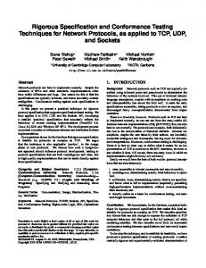
A single particle can hit either the combinational logic or the sequential logic in the silicon [8]. Figure 1 illustrates a typical circuit topology found in nearly all sequential circuits. The data from the first latch is typically released to the combinatorial logic on a falling or rising clock edge, at which time logic operations are performed. The output of the combinatorial logic reaches the second latch sometime before the next falling or rising clock edge. At this clock edge, whatever data happens to be present at its input (and meeting the setup and hold times) is stored within the latch.
All of them have their own space in the market, as each application requires different constraints. But because the semiconductor industry trends to emphasize time-to-market and low-cost production, the implementations based on high-level design look more interesting. In this work, both architectural and the high-level methods are presented and discussed, but because of the high cost of the implementations of the architecture based one, only implementations based on high-level were designed and tested in details.
upset 1
This paper is organized as follows. Section 2 describes the radiation effects on integrated circuits manufactured using CMOS process and it explains in detail the difference between the effects of a SEU in ASIC and in SRAM-based FPGA architectures. Section 3 discusses some SEU mitigation techniques that can be applied at the FPGA architectural level. Section 4 defines the problem of protecting SRAM-based FPGAs against radiation in the high level description. Section 5 introduces a new high-level technique for designing fault-tolerant systems for SRAM-based FPGAs, without modifications in the FPGA architecture, able to cope with transient faults in the user combinational and sequential logic, while also reducing pin count, area and power dissipation compared to the traditional TMR. The main conclusions and future work are discussed in section 6, followed by the references.
IN
upset 2
Combinational logic
OUT
clk
Figure 1. Upsets hitting combination and sequential logic When a charged particle strikes one of the sensitive nodes of a memory cell, such as a drain in an off state transistor, it generates a transient current pulse that can turn on the gate of the opposite transistor. The effect can produce an inversion in the stored value, in other words, a bit flip in the memory cell. Memory cells have two stable states, one that represents a stored '0' and one that represents a stored '1.' In each state, two transistors are turned on and two are turned off (SEU target drains). A bit-flip in the memory element occurs when an energetic particle causes the state of the transistors in the circuit to reverse. This effect is called Single Event Upset (SEU) or soft error and it is one the major concerns in digital circuits.
2. RADIATION EFFECTS ON SRAM-BASED FPGAS The radiation environment is composed of various particles generated by sun activity [5]. The particles can be classified as two major types: (1) charged particles such as electrons, protons and heavy ions, and (2) electromagnetic radiation (photons), which can be x-ray, gamma ray, or ultraviolet light. The main sources of charged particles that contribute to radiation effects are protons and electrons trapped in the Van Allen belts, heavy ions trapped in the magnetosphere, galactic cosmic rays and solar flares. The charged particles interact with the silicon atoms causing excitation and ionization of atomic electrons.
When a charged particle hits the combinational logic block, it also generates a transient current pulse. This phenomenon is called single transient effect (SET) [9]. If the logic is fast enough to propagate the induced transient pulse, then the SET will eventually appear at the input of a latch, where it may be interpreted as a valid signal. Whether or not the SET gets stored as real data depends on the temporal relationship between its arrival time and the falling or rising edge of the clock. In [10], the probability of a SET becoming a SEU is discussed. The analysis of SET is very complex in large circuits composed of many paths. Techniques such as timing analysis [11] could be applied to analyze the probability of a SEU in the combinational logic being stored by a memory cell or resulting in an error in the design operation. Additional invalid transients can occur at the combinatorial logic outputs as a result of SETs generated within global signal lines that control the function of the logic. An example of this would be SETs generated in the instruction lines to an ALU (Arithmetic Logic Unit).
When a single heavy ion strikes the silicon, it loses its energy via the production of free electron hole pairs resulting in a dense ionized track in the local region. Protons and neutrons can cause nuclear reaction when passing through the material. The recoil also produces ionization. The ionization generates a transient current pulse that can be interpreted as a signal in the circuit causing an upset. At the ground level, the neutrons are the most frequent cause of upset [6]. Neutrons are created by cosmic ion interactions with the oxygen and nitrogen in the upper atmosphere. The neutron flux is strongly dependent on key parameters such as altitude, latitude and longitude. There are high-energy neutrons that interact with the material generating free electron hole pairs and low energy neutrons. Those neutrons interact with a certain type of Boron present in semiconductor material creating others particles. The energized alpha particles are the greatest concern in this case and they are addressable through processing and packaging material. In principle, a very careful selection of materials can minimize
In FPGAs, the upset has a peculiar effect when hit the combination and sequential logic mapped into the programmable architecture. Let’s take for example the SRAM-based FPGAs such as the Virtex® family from Xilinx that is one of the most popular programmable devices used in the market nowadays.
420
routing. An upset in the LUT memory cell modifies the implemented combinational logic, figure 3(b). It has a permanent effect and it can only be corrected at the next load of the configuration bitstream. The effect of this upset is related to a stuck-at fault (one or zero) in the combinational logic defined by that LUT. This means that an upset in the combinational logic of a FPGA will be latched by a storage cell, unless some detection technique is used. An upset in the routing can connect or disconnect a wire in the matrix, see figure 3(a). It has also a permanent effect and its effect can be mapped to an open or a short circuit in the combinational logic implemented by the FPGA. The fault will also be corrected at the next load of the configuration bitstream.
Virtex® devices [12] consist of a flexible and regular architecture composed of an array of configurable logic blocks (CLBs) surrounded by programmable input/output blocks (IOBs), all interconnected by a hierarchy of fast and versatile routing resources. The CLBs provide the functional elements for constructing logic while the IOBs provide the interface between the package pins and the CLBs. The CLBs are interconnected through a general routing matrix (GRM) that comprises an array of routing switches located at the intersections of horizontal and vertical routing channel. The Virtex matrix also has dedicated memory blocks called Block SelectRAMs of 4096 bits each, clock DLLs for clock-distribution delay compensation and clock domain control, and two 3-State buffers (BUFTs) associated with each CLB.
When an upset occurs in the user sequential logic synthesized in the FPGA, it has a transient effect, because an upset in the flipflop of the CLB is corrected by the next load of the flip-flop. An upset in the embedded memory (BRAM) has a permanent effect and it must be corrected by fault tolerant techniques applied in the architectural or in the high-level description, as the load of the bitstream cannot change the memory state without interrupting the normal operation of the application. In [13, 14], the effects of upsets in the FPGA architecture are also discussed. Note that there is also the possibility of having single event transient (SET) in the combinational logic used to build the CLB such as input and output multiplexors used to control part of the routing.
Virtex devices are quickly programmed by loading a configuration bitstream (collection of configuration bits) into the device. The device functionality can be changed at anytime by loading in a new bitstream. The bitstream is divided into frames and it contains all the information to configure the programmable storage elements in the matrix located in the Look-up tables (LUT) and flip-flops, CLBs configuration cells and interconnections, figure 2. All these configuration bits are potentially sensitive to SEU and consequently they were our investigation targets. In an ASIC, the effect of a particle hitting either the combinational or the sequential logic is transient; the only variation is the time duration of the fault. A fault in the combinational logic is a transient logic pulse in a node that can disappear according to the logic delay and topology. In other words, this means that a transient fault in the combinational logic may or may not be latched by a storage cell. Faults in the sequential logic manifest themselves as bit flips, which will remain in the storage cell until the next load.
Radiation tests performed in Xilinx FPGAs [15, 16] show the effects of SEU in the design application and prove the necessity of using fault-tolerant techniques for space applications. A faulttolerant system designed into SRAM-based FPGAs must be able to cope with the peculiarities mentioned in this section such as transient and permanent effects of a SEU in the combinational logic, short and open circuit in the design connections and bit flips in the flip-flops and memory cells. In [17], the effect of neutrons was also analyzed in a SRAM-based FPGA from Xilinx. In that time, the FPGA presented very low susceptibility to neutrons, but the vulnerability is increasing as the technology is reaching smaller transistor size and consequently higher logic density.
On the other hand, in a SRAM-based FPGA, both the user’s combinational and sequential logic are implemented by customizable logic memory cells, in other words, SRAM cells, as represented in figure 2. When an upset occurs in the combinational logic synthesized in the FPGA, it corresponds to a bit flip in one of the LUTs cells or in the cells that control the
BlockRAM F1 F2 F3 F4
LUT M
ff
M
M M M M
M
M
Configuration Memory Cell
SEU (Bit flip)
Figure 2. SEU Sensitive Bits in the CLB Tile Schematic
421
Virtex (Xilinx)
CLB
CLB
CLB
CLB
CLB
Several SEU mitigation techniques have been proposed in the last few years in order to avoid faults in digital circuits, including those implemented in programmable logic. They can be classified as: fabrication process-based techniques, such as: epitaxial CMOS processes and advanced process such as silicon-on-insulator (SOI); design-based techniques for mitigation, such as: triple modular redundancy (TMR), time redundancy, multiple redundancy with voting, EDAC (error detection and correction coding) and hardened memory cell level; and recovery techniques (applied to programmable logic only), such as: reconfiguration, partial configuration, rerouting design. However, in the case of SRAM based FPGAs, the problem of finding an efficient technique in terms of area, performance and power is very challenging, because of the high complexity of the architecture. As previously mentioned, when an upset occurs in the user’s combinational logic implemented in an FPGA, it provokes a very peculiar effect not commonly seen in ASICs. The SEU behavior is characterized as a transient effect, followed by a permanent effect. The upset can affect either the combinational logic or the routing. The consequences of this type of effect, a transient followed by a permanent fault, cannot be handled by the standard fault tolerant solutions used in ASICs, such as Error Detection and Correction Codes (EDAC), hamming code, or the standard TMR with a single voter, because a fault in the encoder or decoder logic or in the voter would invalidate the technique. The problem of protecting SRAM-based FPGAs against SEU is not yet solved and more studies are required to reduce the limitation of the methods currently used.
CLB
(a) Upset in the routing (undesirable connection) A
B
C
D
1 1 1 0 0 1 0
In the architectural level, the previous solutions leave open at least two problems to be solved:
0 0
how to cope with SETs in the CLB logic to avoid upsets being stored in the flip-flop,
1 1 1
how to cope with multiple bit upsets in the LUTs, routing and especially in the embedded memory.
1 0
In this section, we propose the investigation and development of SEU mitigation techniques for SRAM-based FPGAs that can be applied to FPGAs with or without embedded processors that can cope with the two problems still not solved. The SRAM based FPGAs were chosen because of their high applicability in space. Different than FPGAs programmed by anti-fuse that can be programmed just once, SRAM based FPGAs can be reprogrammed by the user as many times as necessary in a very short period. So, applications can be updated and corrected after launch. This feature is very valuable for space applications because it can reduce the cost in update missions or even save missions that were launched with design problems.
0 1
(b) Upset in the LUT (modification of the logic) Figure 3. Examples of upsets in the SRAM-based FPGA architecture
3. ARCHITECTURAL SET AND SEU MITIGATION TECHNIQUES FOR SRAM-BASED FPGAS The first SEU mitigation solution that has been used for many years in spacecraft was shielding, which reduces the particle flux to very low levels but it does not completely eliminate it. This solution was sufficient to avoid errors caused by radiation effects for many years in the past. However, due to the continuous evolution of the fabrication technology process, as explained previously, the electronic circuits are becoming more and more sensitive to radiation particles, and the charged particles that once were negligible are now able to cause errors in the electronic design. Consequently, extra techniques must be applied to avoid radiation effects.
First, it is necessary to analyze the amount of the sensitive area in the programmable matrix and the characteristics of them to propose improvements in the SEU mitigation techniques for SRAM-based FPGAs. Figure 2 had shown the set of configuration cells in a CLB tile of the Virtex family. There are 864 memory bits responsible for the customization of the logic. Analyzing the percentage of each type of SRAM cell in the whole set of memory elements in the CLBs, the LUTs represent 7.4%, the flip-flops represent 0.46%, the customization bits in the CLB represent 6.36% and the general routing represents 82.9%, figure 4.
422
7.4%
The hardened memory solution is suitable to replace the SRAM cells in the routing, general customization and lookup tables because they present a small overhead compared to logic redundancy technique and EDAC. Solutions such as IBM [21], NASA [22], DICE [18], HIT [23] and resistor [24] memory cells look interesting in the number of transistors and fault coverage. The final area will be around 2 times the original one, which is a very good result in terms of high-reliability.
0.46% 6.36%
82.9%
LUTs Flip-flops Customization Routing
For the LUT, for instance, if the cells are placed too close to each other, it is possible to use the solution of a TMR memory cell, where each cell is a DICE memory cell. In this case, this solution is robust to the 1st, 2nd and 3rd order of upsets. And because the LUT cells comprise only 7.4% of the cells, the impact in area will not be so intense. In [25], a SEU immune memory cell based on decoupling resistors was developed for FPGAs. The design is asymmetric to provide that the data cell powers-up in a know state. In the referenced paper, the size and the speed of the cell are discussed. The cells are not in the critical path, such as the cells that control de routing, for example, do not need a high-speed. In this case, the tolerance and the size are the main issue. Results show the high reliability of the cell for heavy ions strike.
Figure 4. Percentage of sensitive SRAM bits in the CLB of Virtex FPGAs. Based on these results, the effect of an upset in the routing configuration (customization bits of the CLB and general routing) seems to be the major concern, totaling approximately 90% of the sensitive area in each CLB. This type of fault, as mentioned previously, has a permanent effect, which represents an open or short circuit in the final connections of the logic design. A solution that can increase the area of this customization logic too much is not very attractive in final area and cost of this FPGA. In addition to these programmable cells presented in figure 4, there are other memory elements in FPGA devices that can also be affected by SEU: SelectMAP (Selectable Microprocessor Access Port) latches, JTAG (Joint Test Action Group - IEEE Std. 1149.1x), TAP (Test Access Port) latches and others latches of other built-in non-programmable features. The main effects of a SEU in these latches are SEFI (Single Event Functional Interrupt) such as configuration circuit upsets and JTAG circuit upsets. There are few flip-flops or latches in the POR, less than 40 latches or flip-flops, which leads to a very small cross-section. But they cannot be disregarded because an upset in one of these latches can force the chip to be reprogrammed.
The embedded memory in the FPGA must be protected in order to avoid errors. EDAC is a suitable technique to correct upsets in memory structures, as discussed previously. An example is the hamming code that can be applied to embedded FPGA memory. However, hamming code is not able to cope with multiple upsets in the same coded word. And in the case of the embedded memory, it is very important to protect the cells against multiple bit upsets (MBU) for two main reasons: new SRAM technologies (VDSM) are susceptible to MBU, the scrubbing procedure does not reconfigure (update) the internal memory, and consequently, upsets have a higher probability of accumulating in the memory. So, a new code is needed to correct all possible double errors. The initial option would be using a Reed-Solomon code with capability to correct two different symbols. But this RS code has more than twice the area and delay overhead of the single symbol correction RS [26], which makes this solution inappropriate for hardware implementation in memory architectures. Previous work has been published on the use of RS code to protect memory [27], however it does not take into account double bit upsets in the same coded word, which is likely to occur in VDSM technologies.
Some solutions to protect the POR can be: TMR the whole block, replace the cells by SEU hardened memory cells or use extra logic to turn off the POR after the device is programmed by an external pin. In the next paragraphs, some fault-tolerant techniques will be discussed to protect the SRAM cells of the LUT, flip-flops, routing and customization cells, and the embedded block RAM. The advantages and disadvantages of each technique were analyzed based on previous work results in ASICs implementations.
An innovative solution has been developed able to correct all double bit upsets in VDSM memories [28]. This solution combines hamming code and RS code with single symbol correction capability. This technique solves the problem of how to achieve 100% of double fault correction with a low-cost RS code. The hamming code protects the bits between the RS symbols. The number of bits protected by hamming will be the same as the number of symbols protected by Reed-Solomon, so this option does not significantly increases the area overhead.
The first solution that can be studied is to replace some or all of the latches in the FPGA by SEU hardened flip-flops. Many hardened memory cells were designed during the last years. However each one has different characteristics that can show more efficiency for some applications. They differ from each others in some characteristics such as: the number of transistor, the method, the SEU order effect, the ability to accumulate or not upsets and the SET immunity in combinational logic. For example, standard latches have a first order of susceptibility; in other words, they are upset by a single node strike. Some of them require multiple node strikes to upset cells such as TMR memory cells, DICE memory cell [18] and simple temporal memory cells [19]. Temporal latches built from DICE cells, for example, have a second and third order of susceptibility [20], which means that is robust to upsets in multiple memory cells and also a ion strike in multiple nodes of a single cell.
The triple modular redundancy (TMR) is another SEU mitigation technique. There are many TMR topologies. Each implementation is associated with different area penalties and fault coverage. The system requirements and the architecture must be analyzed in order to correctly choose the most convenient approach. Now, let’s take a look in the CLB flip-flops. They receive the output of the multiplexors that set up the signal path from the
423
compared through a majority vote circuit. The TMR technique for Virtex® is presented in details in [31], and more examples are also presented in [32]. The correct implementation of TMR circuitry within the Virtex architecture depends on the type of data structure to be mitigated. The logic may be grouped into four different structure types: Throughput Logic, State-machine Logic, I/O Logic, and Special Features (SelectRAM block, DLLs, etc.). The TMR technique for Virtex is illustrated in figure 6.
LUT in the CLB slice. If a transient fault (SET) occurs in one of the multiplexors, this upset must not be stored in the flip-flops. Consequently, it is not sufficiently reliable to replace the CLB flip-flop by a hardened flip-flop. It is also necessary to insert some kind of fault detection and correction in the input of this flip-flop to filter SETs. The combinational logic does not need to be changed. A possible solution is to combine the temporal latch composed of DICE memory cells, presented in [20] with the TMR approach with refreshing. The final flip-flop shows a high reliability to 1st, 2nd and 3rd order of SEU and SETs, refreshing of SEU and additionally a small impact in the final area because the flip-flops correspond to less than 1% of the total sensitive area. Figure 5 shows this hardened flip-flop topology.
IN
The scrubbing [30] allows a system to repair SEUs in the configuration memory without disrupting its operations. The scrubbing is performed through the Virtex® SelectMAP interface. When the FPGA is in this mode, an external oscillator generates the configuration clock that drives the PROM and the FPGA. At each clock cycle new data are available on the PROM data pins. One example is the Flash-PROM XQR18V04 that provides a parallel frequency up to 264 Mbps at 33 MHz.
clk
The scrubbing cycle time depends on the configuration clock frequency and on the readback bitstream size. For the XQVR300, it is necessary to utilize 207,972 clock cycles in order to perform the full scrubbing load (Scrub cycle = # clock cycles x clock period). The scrubbing rate describes how often a scrubbing cycle must occur. It is determined by the expected upset rate of the device for the given application. Upset rates are calculated from the static bit cross-section of the device and the charged particle flux the application or mission is expected to endure. The scrubbing rate should be set such that any SEU on the configuration memory will be fixed before the next upset will occur. In reality the scrubbing rate is minimized to be equal to the scrubbing cycle. In this way configuration logic is always being refreshed. The implemented design can also have influence in the selection of the scrubbing rate. A good "rule of thumb" is to place the scrubbing rate one order of magnitude or more above the expected upset rate. In other words, the system should scrub, on the average, at least ten times between upsets.
MAJ
clk+d
clk+2d clk+2d+tp Dice cell
Figure 5. Proposed SEU and SET Hardened flip-flop with refreshing
4. HIGH-LEVEL SEU MITIGATION TECHNIQUES FOR SRAM-BASED FPGAS BASED ON TMR The previous section discussed fault-tolerant techniques in the architectural level for SRAM-based FPGAs. Although these solutions can achieve a high reliability, they also present a high cost because they need investment in development, test and fabrication. So far, there are very few FPGA companies that are investing in designing fault-tolerant FPGAs as this market is still focused in only military and space application, which is very small compared to the commercial market. However, because of the technology evolution, applications at the atmosphere and at ground level have been starting to face the effect of neutrons, as mentioned in section 2. As a result, fault-tolerant techniques begin to be necessary in many commercial applications that need some level of reliability.
The fault injection analysis results show that the “golden” TMR method has presented “no errors” in presence of single bit upset in the Virtex bitstream. This report demonstrates the efficiency of the TMR SEU mitigation technique for SRAM-based FPGAs. Radiation ground testing performed in the “golden” chip TMR methodology in the counter design confirmed the results achieved by the fault injection experiment. The fault injection results in the TMR 8051-like micro-controller were meaningful to continue the validation of this technique and it has confirmed the reliability of the Virtex TMR design techniques. The radiation test of the TMR 8051 micro-controller has shown the efficiency of the TMR mitigation technique to a large set of space applications.
A less expensive solution is a high-level SEU tolerant technique that can be easily implemented by the user or by the company designers in commercial FPGAs or in parts manufactured by a technology that can avoid latch up and reduce the total ionization dose, as the Virtex® QPRO family [29]. The high-level SEU mitigation technique used nowadays to protect designs synthesized in the Virtex® architecture is mostly based on TMR combined with scrubbing [30]. The TMR mitigation scheme uses three identical logic circuits (redundant block 0, redundant block 1 and redundant block 2), synthesized in the FPGA, performing the same task in tandem, with corresponding outputs being
In summary, it is important to remark that there is a possibility of an upset if the routing connects two different modules of the TMR, but it is very low. The probability is related to the routing density and logic placement. Dedicated floorplanning for each redundant module of the TMR can reduce the probability of upsets in the routing affecting two or more logic modules. Table 1 summarizes the effect of a fault in each FPGA module in the TMR design with no assigned area constraint floorplanning.
424
Sequential logic (flip-flops triplicated + majority voters)
Corrected by voter
3x input pads tr0
clk0
…
Corrected by scrubbing
tr1
clk1
tr2
clk2
check0
tr0
MAJ
MAJ
tr1
check1
tr2
check2
… MAJ
3x output pads with minority voters
Combinational logic triplicated
Figure 6. Triple Modular Redundancy for Xilinx FPGAs Table 1. Upsets Analysis in the Triple Modular Redundancy Approach with No Assigned Area Constraint Floorplanning Upset Location LUT Routing
Action Modification in the Combinational logic Connection or disconnection between any two signals in the design
Customization logic in general
Connection or disconnection between any two signals in the same CLB
Flip-flops
Modification in the sequential logic
Consequences - Error in the redundant part with no error in the TMR design output - Error in the redundant part with no error in the TMR design output - Error in more than one redundant parts with error in the design output - Error in the redundant part with no error in the TMR design output - Error in more than one redundant parts with error in the design output - Error in the redundant part, no error in the TMR design output
Upset Correction By Scrubbing By scrubbing
By Scrubbing
By user correction technique (VHDL)
The reliability and the safety of TMR scheme compared to selfchecking-based fault-tolerant schemes were discussed in [33]. The experimental results presented that the higher the complexity of the module, the greater the difference in reliability between self-checking and TMR. In summary, the self-checking faulttolerant scheme can achieve a higher reliability in comparison to the TMR if the self-checking overhead bound of 73% is not exceeded. The idea of using self-checking fault-tolerant scheme can be extended for FPGAs by using the duplication with comparison (DWC) method combined with concurrent error detection (CED) technique that it works as a self-checking. Figure 7 presents the scheme, called hot backup DWC-CED. The CED is able to detect which module is faulty in the presence of an upset, and consequently, there is always a correct value in the output of the scheme, because the mechanism is able to select the correct output out of two.
5. REDUCING TMR OVERHEADS BY COMBINING HARDWARE AND TIME REDUNDANCY The TMR technique is a suitable solution for FPGAs because it provides a full hardware redundancy, including the user’s combinational and sequential logic, the routing, and the I/O pads. However, it comes with some penalties because of its full hardware redundancy, such as area, I/O pad limitations and power dissipation. Many applications can accept the limitations of the TMR approach but some cannot. Aiming to reduce the number of pins overhead of a full hardware redundancy implementation (TMR), and at the same time coping with permanent upset effects, we present a new technique based on time and hardware redundancy to protect the user’s combinational logic, where the double modular redundancy with comparison (DWC) is combined with a time redundancy upset detection machine, able to detect upsets and to identify the correct value to allow continuous operation. The sequential logic continues to be protected by TMR to avoid accumulation of faults as previously described, since the scrubbing does not change the content of a user’s memory cell. However, experiments based on using duplication for both combinational and sequential logic for digital filters have shown high reliability, as it will be discussed further in this paper.
In the case of SEU detection in SRAM-based FPGAs, the CED must be able to identify permanent faults in the redundant modules. The CED works by finding the property of the analyzed logic block that can help to identify an error in the output in the presence of a permanent fault. There are many methods to implement logic to detect permanent faults, most solutions are based on time or hardware redundancy and they manifest a property of the logic block that is being analyzed.
425
Combinational logic
The combination of DWC technique and CED blocks enabling one to detect permanent faults provides a new high-level SEU mitigation technique for FPGAs. Two clock cycles are needed to identify a permanent fault in the combinational logic module. However, this extra time does not occur at every clock operation in our approach. Using DWC combined with CED for permanent faults, it is possible to take advantage of the simple comparison at the output of the duplication scheme to inform whether it is necessary to re-compute the data for permanent fault detection. The re-computation is needed only when a mismatch of the outputs occurs. This method has been named duplication with comparison combined to concurrent error detection block (DWCCED).
Sequential logic
dr0
TMR
CED CED Permanent fault detection
dr1
Figure 7. DWC combined with CED scheme The CED scheme based on time redundancy recomputes the input operands in two different ways to detect permanent faults. During the first computation at time t0, the operands are used directly in the combinational block and the result is stored for further comparison. During the second computation at time t0+d, the operands are modified, prior to use, in such a way that errors resulting from permanent faults in the combinational logic are different in the first calculation than in the second and can be detected when results are compared. These modifications are seen as encode and decode processes and they depend on the characteristics of the logic block. The scheme is presented in figure 8.
Figure 9 shows the scheme proposed for an arithmetic module, in the present case study: a multiplier. There are two multiplier modules: mult_dr0 and mult_dr1. There are multiplexors at the output able to provide normal or shifted operands. The output computed from the normal operands is always stored in a sample register, one for each module. Each output goes directly to the input of the user’s TMR register. Module dr0 connects to register tr0 and module dr1 connects to register tr1. Register tr2 will receive the module that does not have any fault. By default, the circuit starts passing the module dr0. A comparator at the output of register dr0 and dr1 indicates an output mismatch (Hc). If Hc=0, no error is found and the circuit will continue to operate normally. If Hc=1, an error is characterized and the operands need to be re-computed using the RESO method to detect which module has the permanent fault. The detection takes one clock cycle.
Time t=t0 Combinational logic
encoder
Combinational logic
comparator
clk
Time t=t0+d
error
In the case of a registered output, each output goes directly to the input of the user’s TMR register. Figure 10(a) illustrates the logic scheme. Module dr0 connects to register tr0 and module dr1 connects to register tr1. While the circuit performs the detection, the user’s TMR register holds its previous value. While the circuit performs the detection, the TMR register holds its previous value. When the faulty free module is found, register tr2 receives the output of this module and it will continue to receive this output until the next chip reconfiguration (fault correction). By default, the circuit starts passing the module dr0. In the case of a non-registered output, the signals can be driven directly to the next combinational module or to the I/O pads, as shown in figure 10(b).
decoder output
Figure 8. Time redundancy for permanent fault detection If an output mismatch occurs, the output register will hold its original value for one extra clock cycle, while the CED block detects the permanent fault. After this, the output will receive the data from the fault free module until the next reconfiguration (fault correction). The important characteristic of this method is that it does not incur a high performance penalty when the system is operating free of faults or with a single fault. The method just needs one clock cycle in hold operation to detect the faulty module, and after that it will operate normally again without performance penalties. The final clock period is the original clock period plus the propagation delay of the encoders, decoders and output comparator.
Let’s consider two different fault situations when the output is saved in a TMR register. In one, the fault occurs in module dr0 (Mult_dr0). Hc indicates that there is an output mismatch; Tc0 indicates that module dr0 is faulty and Tc1 indicates that dr1 is fault free. This analysis takes one clock cycle. Consequently, the permanent fault detection block selects dr1 for the tr2 input. Note that the value stored in the user’s TMR register is held for one cycle while the scheme identifies the faulty free module. In the second case, a fault occurs in the module dr1 (Mult_dr1), similar to the previous example, Hc indicates that there is an output mismatch; Tc0 indicates that module dr0 is fault free and Tc1 indicates that dr1 is faulty. The permanent fault detection block selects dr0 for the tr2 input.
Many techniques to encode and decode were proposed in the literature to detect permanent faults [34, 35, 36] (JOHNSTON; AYLOR; HANA, 1988; PATEL; FUNG, 1996; AVIZIENIS, 1971), some based on time redundancy, such as bit-wise inversion, re-computing with shift operands (RESO) and recomputing with swapped operands (REWSO); and some based on hardware redundancy, such as parity prediction and module code.
426
B
A encode ST0
1
B
encode 0
1
A encode
0
0
dr0
decode
0
ST1
1
dr1
clk1
dr0
1
encode
clk0
=
=
Tc0
decode
dr1 =
Hc
Tc1
voter Enable faulty free module
ST0
ST1
Figure 9. Fault tolerant technique based on DWC combined with CED for SRAM-based FPGAs dr0 dr1 dr0
tr0
clk0
MAJ
Enable faulty free module
dr1
tr1 MAJ
clk1
tr2
pad
dr0 Enable faulty free module
clk2+d
dr1
MAJ
pad
(a) Combinational output registered
(b) Combinational output in the pad
Figure 10 – Examples of implementations with the combinational output registered and in the pads In the proposed method, the area reduced by the design compared to the TMR is the area of one user’s combinational logic module and the number of inputs that is reduced from 3 times to 2 times the original number. This technique can be used as an additional option for the TMR technique for designing reliable circuits in FPGAs with pads and power reduction. Because the combinational circuit is just duplicated, inputs and outputs can be duplicated instead of triplicated, as in the TMR approach. However, it is important to notice that the TMR inputs related to the user’s sequential logic used in the CLB flip-flops are not changed as triple clocks, reset, etc.
Note that in both methods, TMR and the proposed technique, the upsets in the user’s combinational logic are corrected by scrubbing, while upsets in the user’s sequential logic are corrected by the TMR scheme used in the CLB flip-flops. It is important to notice that for upset correction the scrubbing is performed continuously, to guarantee that only one upset has occurred between two reconfigurations in the design. Some constraints must be observed for the perfect functioning of the technique, same as TMR: there must not be upsets in more than one redundant module, including the state machine detection and voting circuit, consequently it is important to use some assigned area constraints to reduce the probability of short circuits between redundant module dr0 and dr1. The scrubbing rate should be fast enough to avoid accumulation of upsets in two different redundant blocks. Upsets in the detection and voting circuit do not interfere with the correct execution of the system, because the logic is already triplicated. In addition, upsets in the latches of this logic are not critical, as they are refreshed in each clock cycle. Assuming a single upset per chip between scrubbing, if an upset alters the correct voting, it does not matter, as long as there is no upset in both redundant blocks.
In addition, the advantage of using this technique is not only focused in reducing the pin count and the number of CLBs, but also in other types of radiation effects such as total ionization dose, as this method has the important characteristic of detecting permanent faults. So far, we have mentioned only SEUs that happen in the SRAM programmable cells that are permanent until the next reconfiguration. However, a circuit operating in the space environment can suffer from total ionization dose and other
427
RESWO was not used because some operations performed by the ALU are not commutative, like subtraction, increment or decrement.
effects that can provoke permanent physical damages in the circuit.
5.1 Analyzing the Concurrent Error Detection Techniques
A canonical FIR filter circuit was chosen as a sequential case study for the proposed technique. The multipliers were designed with constant coefficients, resulting in an optimized area and minimal faulty nodes. An 8-bit FIR canonical filter of 9 taps was automatically generated. The multiplier coefficients are: 2, 6, 17, 32 and 38. There is an 8-bit input; consequently, there are 28 = 256 combinations of input vectors to test. The total of faulty nodes in the FIR filter, including all its multipliers and adders is 4208. All the possible combinations of input vectors and faults were tested, totaling 1,077,248.
Many techniques to the encoder and decoder blocks were proposed in the literature to detect permanent faults by recomputation [34, 35, 36], some based on time redundancy, such as bit-wise inversion, re-computing with shift operands (RESO) and re-computing with swapped operands (REWSO); and some based on hardware redundancy, such as parity prediction and residue code. The goal is to investigate each one in terms of fault detection, area and performance penalties and to select the most appropriated ones for each type of circuit. In order to evaluate the fault coverage of these techniques, some combinational and sequential circuits were tested, including an 8-bit multiplier, arithmetic and logic unit (ALU), and a FIR canonical filter.
The faults were exhaustively injected in all nodes of the case studied circuits for each input vector, sensitive node and redundant module (mult_dr0 or mult_dr1). The fault injection system operates with two clocks, one to control the change of the input vectors and other one to control the change of the faults. A counter controls the total number of combinations of input vectors and faults that must be inserted in the circuit. All combinations have been injected. There is a signal to indicate when the fault injection is done.
The multipliers and filters protected by DWC-CED were automatically generated by the developed tools Lemon Dragon multiplier and filter generator. In addition, in order to enable the fault injection in high-level, an automatic generation of fault injection structures was also developed. All nodes in the design were replaced by one fault injection component, so that the user may insert as many faults as needed. The component is a 4 to 1 multiplexor. If the select signal of the multiplexor is 00, the original signal is passed to the output; if select is 01, the constant 0 is the output (stuck-at 0); if select is 10, the constant 1 is propagated (stuck-at 1).
In all cycles, the outputs of the gold circuit (module dr0) and the DUT (module dr1) are compared. If the outputs are equal (Hc=0), this means that if there is a fault in one of the circuits, the fault did not generate an error in the output, so for real time operation proposes, this fault can be ignored and no detection operation must be performed. If a fault has generated an error in the output (Hc=1), the output of module dr1 is compared with the decoded output of the recomputing circuit (copy of module dr1). If the outputs are not equal (Tc1=1), this means that the technique currently used was able to detect the fault. At the same time, the output of module dr0 is compared to the decoded output of the recomputing circuit (copy of module dr0). If the outputs are equal (Tc0=0), this means that the technique was able to detect a faultfree module.
An 8-bit multiplier was the first case study. All techniques presented were implemented on this circuit: residue code, using hardware redundancy; RESWO, 1-shift RESO with 8 bits (ignoring the left bit) and 9 bits (expanding the operands), 2-shift RESO with 8 and 9 bits, and residue code, using time redundancy. The multipliers were implemented using cascaded full adders (FA). For the 8-bit multiplier, there are 528 faulty nodes, 1056 faults in total (stuck-at 0 or 1), and for the 9-bit multiplier, 675 nodes, 1350 faults in total. In both cases, the two original operands have 8 bits, resulting in 216 (65,536) combinations of input vectors. All combinations of faults and input vectors were injected, totaling 69,206,016 for the 8-bit version and 88,473,600 for 9-bit one.
An undetected fault is characterized when there is a mismatch in the output of dr0 and dr1 (Hc=1) and the technique was not able to detect the faulty module (status Tc1=0) or it was not able to detect the fault-free module (status Tc0=1). A counter is incremented to show the number of total undetected faults. After all, this counter is read from the prototyped board and the percentage of undetected faults is calculated. The results in numbers and percentage of detected faults are in table 2.
The next case study was an Arithmetic and Logic Unit (ALU). This ALU performs the following operations: addition, subtraction, increment, decrement, AND, OR, XOR and NOT. This ALU was designed in a bit slice approach and it has two 8bit input operands, plus a 4-bit selection. Then, there are 220 = 1,048,576 combinations of input vectors to be tested. Each slice has 16 faulty nodes, resulting in 256 different faults for an 8-bit ALU. All the combinations were injecting, totaling 268,435,456. At this time not all techniques were evaluated. The method
Results show that all variations of RESO had better results in terms of fault coverage than residue code using time redundancy and RESWO.
428
Table 2. Fault Coverage of CED techniques in SRAM-based FPGAs Circuit
8-bit Multiplier
8-bit ALU
8-bit Filter
CED Technique Residue-15 (hard) Residue-15 (time) RESWO RESO 8 bits RESO 9 bits 2-shift RESO 8 bits Residue-15 (hard) Residue-15 (time) RESO 8 bits RESO 9 bits 2-shift RESO 8 bits 2-shift RESO 9 bits Residue-15+RESO-9bits Residue-15 (hard) Residue-15 (time) RESO 8 bits
# of injected faults 69,206,016 69,206,016 69,206,016 69,206,016 88,473,600 69,206,016 268,435,456 268,435,456 268,435,456 268,435,456 268,435,456 268,435,456 268,435,456 1,077,248 1,077,248 1,077,248
# of detected faults 69,136,448 47,387,924 48,458,171 69,176,011 88,473,600 69,198,150 222,135,593 199,912,813 213,005,264 245,694,848 213,048,871 245,763,385 248,907,886 1,077,248 718,105 1,077,248
% of detected faults 99.89 68.47 70.02 99.95 100.00 99.98 82.75 74.47 79.35 91.52 79.36 91.55 92.72 100.00 66.66 100.00
also area. Note that the 16x16 bits multiplier protected by TMR could not be synthesized in the prototype board that uses a Virtex part with 240 I/O pins (166 available for the user); while the same multiplier, implemented by the proposed technique could fit in the chip, and also occupy less area. In terms of performance, the TMR approach has presented an estimated frequency of 33.8 MHz, while the DMR-CED approach has presented a frequency of 26.7 MHz.
One can notice that residue code had higher fault coverage using hardware redundancy than time redundancy. It is because of the using of the same faulty hardware to compute the residue code, there is a high possibility of the coded word having the same effect in the output. RESO is the most appropriate technique in terms of fault coverage for multipliers and consequently all the circuits that use them as filters. For ALU, no one of the presented techniques was suitable enough to guarantee 100% of detection. This happens because the ALU logic is not only composed of arithmetic operations but also logic Boolean functions, where the discussed techniques are not efficient. RESO technique has been chosen to be used as the concurrent error detection technique for the DWC-CED method.
Table 4 presents area results of an 8-bit 9 taps filter, with multiplier coefficients: 2, 6, 17, 32 and 38, using no tolerance technique, TMR technique and the proposed technique. The registers are also protected by TMR, while the combinational logic (multipliers and adders) is protected by DWC-CED using RESO approach. The CED block is placed at the outputs, and it votes the correct pad output from dr0 or dr1. Results show that the 9 taps FIR canonical filter occupies 13% less area in the FPGA if protected by DWC and time redundancy instead of by TMR. The results also present a reduction of 19% in the pin count compared to TMR. In terms of performance, the TMR has presented an estimated frequency of 40 MHz, while the DWC-CED technique has presented a frequency of 22 MHz.
5.2 Area and Performance Results Table 3 presents area results of 8x8 and 16x16 bits multipliers, implemented in the XCV300 FPGA using no fault tolerance technique, TMR technique and the proposed technique (DWCCED for permanent faults using RESO approach). All of the multipliers are synthesized with a register at the output. Results show that according to the size of the combinational logic block, it is possible to not only reduce the number of I/O pins but
Table 3. Comparison of multiplier implementations (XCV300-PQ240) Multipliers Registered output Total of I/O pads Number of 4-LUTs Number of ffs Non-registered output Total of I/O pads Number of 4-LUTs Number of ffs
Standard 8x8 16x16
8x8
34 159 16 8x8 32 156 0
108 584 48 8x8 96 551 0
66 741 32 16x16 64 711 0
TMR 16x16* 204 2285 96 16x16* 192 2159 0
DWC-CED 8x8
16x16
92 (-14%) 534 (-8,5%) 82 (+34) 8x8 66 (-31%) 425 (-23%) 34
172 (-17%) 1791 (-22%) 162 (+66) 16x16 130 (-32%) 1442 (-33%) 66
* I/O pins were out of range, the part XCV300-BG432 was used.
429
Based on the percentage of each type of memory cell in the whole set of memory elements in the CLBs, the LUTs represent 7.4%, the flip-flops represent 0.46%, the customization bits in the CLB represent 6.36% and the general routing represents 82.9%, the probability of an upset affecting the registers is very low compared to the probability of this same upset affecting the logic. In addition, the effect of an upset in a register is not always seen in the final output after being divided by the constant, in the example, the number 512.
Table 4. Digital FIR Filter Implementation XCV300-PQ240 Standard Total of I/O pads Number of 4-LUTs Number of ffs
26 244 64
TMR 84 887 192
The proposed method 68 776 226
In the case of the FIR digital filter, the technique can be additionally improved by using duplication in the registers too. The possibility of using duplication instead of TMR in the sequential logic is due to some characteristics of the filter. The first one is because the data inside the filter is pipelined. At each clock cycle, each register receives a new input that cleans up the upset that is propagated to the next register. In the worst case, it is necessary to wait the n clock cycles of the pipeline to wash out all the upsets. The second characteristic is the use of multiplier coefficients that are multiplied by a constant that usually corresponds to the highest possible input number to avoid floating point multiplications. This implies that the output must be divided by this same constant number, consequently the output is truncated and many upsets in the internal operation are eliminated in the end.
All possible combinations of bit flips for the tested input signal were injected in the registers. In total, 90 bit-flip faults were injected, on at input process. There are 9 bits multiplied by 10 registers, the fault bits from the first register need 10 clock cycles to be washed out, the fault bits from the second register need 9 clock cycles, the fault bits in the third register need 8 clock cycles, and so on. Consequently, the filter is operating with the presence of faults for 495 clock cycles. In order to improve the integrity of the filter output signal, the 7 first tap registers, which are the ones that influence the most the output, had the 3 most significant bits (msb) protected by TMR, including the signal bit. In summary, 21 bits were protected from the total of 90, which represent 23% of the total sensitive bits. This protection reduces to upset effects in the output to a very low level as seen in graphics from the Matlab tool [37]. Table 5 shows a comparison between many SEU hardened filter implementations: the standard version, the TMR version, the filter protected by DWC-CED technique only in the combinational logic, the DWC-CED technique applied in the combinational and sequential logic, and the proposed DWC-CED technique applied in the combinational and in some bits of the sequential logic to improve reliability reducing cost.
The test case is an 11 taps 9-bit digital low-pass filter protected by only DWC-CED in the combinational and sequential logic. The original coefficients calculated by Matlab [37] were multiplied by the constant 512. The final multiplier coefficients are: 1, -1, -9, 6, 73 and 120. There are ten 9-bit registers, totaling 90 bits that can be upset by SEU. An upset can affect the registers, which has a transient effect, or can affect the logic (multipliers, adders, voters), which has a permanent effect. The input waveform has the frequencies 100Hz, 1 KHz and 8 KHz added in the same signal. The frequencies lower than 3.75 KHz are passed to the output without any attenuation, in the example: frequencies 100Hz and 1KHz. Frequencies from 3.75 to 5.625 KHz are attenuated. Frequencies higher than 5.625 are blocked by the filter design.
Results show that for the 11 taps 9-bit FIR canonical filter protected by DMR and efficient TMR in only some bits of the registers occupies 3.5% less area in the FPGA compared with the DMR in the combinational logic and TMR in registers with 60 less flip-flops. Comparing with the full TMR, this new method shows a reduction of 16.5% in area and 22 less flip-flops.
Table 5. Filter Implementation using DWC-CED in the combinational and sequential logic (XCV300-PQ240) Standard Total of I/O pads Number of 4-LUTs Number of ffs
TMR
DWC-CED (combinational)
DWC-CED (all)
DWC-CED (*)
28
84
66
56
56
496
1548
1350
1274
1304
90
270
308
218
248
* 3 bits in the 7 first registers protected by TMR
pads pads
CED
CED
Figure 11. Implementation of the fault tolerant technique based on DWC combined with CED and TMR for SRAM-based FPGAs
430
reduces the number of input and output pins of the user’s combinational logic. In addition, it can also reduce area when large combinational blocks are used.
According to the user’s application requirements, the designer will be able to choose between a full hardware redundancy implementation (TMR) or a mixed solution where duplication with comparison is combined to concurrent error detection to reduce pins and power dissipation in the interface, as well as area, as shown in previous examples. Figure 11 shows some implementations combining TMR and DWC with time redundancy. It is possible to use this new technique only in the interface of the FPGA, in this way reducing pins, or along the design to reduce the number of I/O pads and also area for large combinational circuits, as presented in table 3 and table 4.
The proposed technique can be used as an additional option for the TMR technique for designing reliable circuits in FPGAs with pads and power reduction. Because the combinational circuit is just duplicated, inputs and outputs can be duplicated instead of triplicated, as in the TMR approach. In addition, the advantage of using this technique is not only focused in reducing the pin count and the number of CLBs, but also in other types of radiation effects such as total ionization dose, as this method has the important characteristic of detecting permanent faults.
Sequential circuits such as counters and state machines are more suitable to be protected by TMR, as the combinational logic is small compared to the sequential logic. The proposed technique is an alternate method to protect combinational circuits, as it is necessary to insert a concurrent error detection block. On the other side, large combinational logic blocks can be easily found in many applications. For example, microprocessors are composed of combinational logic such as the Arithmetic and Logic Unit, multipliers and the micro-instruction decoder.
The consideration of using FPGA in space applications is fairly recent and there is still a lot of work to be done in this area. In summary, the main contributions of this work were the detailed analysis of the effects of a single event upset (SEU) in the architecture of a SRAM-based FPGA, the investigation and experiment tests of the state-of-the-art fault-tolerant techniques and the development of new SEU mitigation techniques that improve the reliability and reduce the cost compared to the current solutions presented in the market nowadays. Additionally to what has been mentioned previously, future work also includes the implementation of the DWC-CED technique combined to the TMR technique in a more complex case study, such as the microcontroller 8051, which has arithmetic and random combinational logic, sequential logic and embedded memories. In this case, all the details and techniques will be tested. The final analysis of this new version of the full protected 8051 micro-controller in a FPGA platform will be performed under radiation ground test. The results will guide the research in future developments.
6. CONCLUSIONS This paper presented some studies and developments of SEU mitigation techniques for programmable architectures such as SRAM-based FPGAs. The choice of SRAM based FPGAs is due to their high applicability in apace applications. Because they are reprogrammable, designs can be updated or corrected after launch, which can reduce considerably the mission cost. The Virtex family from Xilinx was chosen to be the case study for this work because is one of the most popular, highest logic density and best performing FPGAs in the market.
ACKNOWLEDGMENTS
Some architectural solutions have been proposed to improve the reliability of the ones currently used nowadays. One of them is the use of RS code combined with hamming code to protect the embedded memory against multiple upsets. This is an innovative solution that can be easily applied to any memory structure to protect against all double bit upsets and a large combination of multiple upsets. This technique was prototyped in a FPGA and results show that the area overhead is acceptable for the reliability achieved. One of the main advantages of this technique compared to the TMR is the low parity bits overhead, which in the case of the TMR is 200% and in the proposed approach varies around 10 to 20%. A drawback of this technique is the performance penalty.
The authors wish to thank Xilinx and CNPq Brazilian Agency for their support of this work and Renato Hentschke from Federal University of RGS in Brazil (UFRGS) for his contribution on the case study circuit description.
REFERENCES [1] Nasa. Radiation Effects on Digital Systems. USA, 2002. Available at: < radhome.gsfc.nasa.gov/top.htm>. Visited on January, 2003. [2] Sia Semiconductor Industry Association. The National Technology Roadmap for Semiconductors. USA, 1994. [3] Johnston, A. Scaling and Technology Issues for Soft Error Rates. In Research Conference On Reliability, 4., 2000. Proceedings... Palo Alto: Stanford University, 2000. [4] O'Bryan, M. et al. Current single event effects and radiation damage results for candidate spacecraft electronics. In IEEE Radiation Effects Data Workshop, 2002. Proceedings... [S.l.]: IEEE Computer Society, 2002. p. 82-105. [5] Barth, J. Applying Computer Simulation Tools to Radiation Effects Problems. In IEEE Nuclear Space Radiation Effects Conference, NSREC, 1997. Proceedings… [S.l.]: IEEE Computer Society, 1997. p. 1-83. [6] Normand, E. Single event upset at ground level. IEEE Transactions on Nuclear Science, New York, v.43, n.6, p. 2742 -2750, Dec. 1996.
Another architectural proposed solution is based on the use of hardened memory cells with SET detection capability to replace the flip-flops located in the CLB in order to avoid bit flips and errors from transient faults in the combinational gates of the CLB, for instance, the multiplexors. This proposed approach can protect the flip-flop against SEU in the 1st, 2nd and 3rd order, and in addition to SET, which is a big concern in the very deep submicron technologies. In terms of high-level fault-tolerant solutions, this work presented a new technique for upset detection and voting that combines duplication with comparison (DWC) with concurrent error detection (CED) based on time redundancy for the user’s combinational logic in SRAM-based FPGAs. This technique
431
[21] Rockett, L. R. An SEU-hardened CMOS data latch design. IEEE Transactions on Nuclear Science, New York, v.35, n.6, p. 1682-1687, Dec. 1988. [22] Whitaker, S.; Canaris, J.; Liu, K. SEU hardened memory cells for a CCSDS Reed-Solomon encoder. IEEE Transactions on Nuclear Science, New York, v.38, n.6, p. 1471-1477, Dec. 1991. [23] Calin, T.; Nicolaidis, M.; Velazco, R. Upset hardened memory design for submicron CMOS technology. IEEE Transactions on Nuclear Science, New York, v.43, n.6, p. 2874 -2878, Dec. 1996. [24] Weaver, H.; et al. An SEU Tolerant Memory Cell Derived from Fundamental Studies of SEU Mechanisms in SRAM. IEEE Transactions on Nuclear Science, New York, v.34, n.6, Dec. 1987. [25] Rockett, L. R. A design based on proven concepts of an SEU-immune CMOS configurable data cell for reprogrammable FPGAs. Microelectronics Journal, Elsevier, v.32, p. 99-111, 2001. [26] Houghton, A. D. The Engineer’s Error Coding Handbook. London: Chapman & Hall, 1997. [27] Redinbo, G.; Napolitano, L.; Andaleon, D. Multi-bit Correcting Data Interface for Fault-Tolerant Systems. IEEE Transactions on Computers, New York, v.42, n.4, p. 433446, Apr. 1993. [28] Neuberger, G.; Lima, F.; Carro, L.; Reis, R. A Multiple Bit Upset Tolerant SRAM Memory. Transactions on Design Automation of Electronic Systems, TODAES, New York, v.8, n.4, Oct. 2003. [29] Xilinx, Inc. QPRO™Virtex®™ 2.5V Radiation Hardened FPGAs: Application Notes 151. USA, 2000. [30] Xilinx Inc. Virtex® Series Configuration Architecture User Guide: Application Notes 151. USA, 2000. [31] Carmichael, C. Triple Module Redundancy Design Techniques for Virtex® Series FPGA: Application Notes 197. San Jose, USA: Xilinx, 2000. [32] Lima, F.; Carmichael, C.; Fabula, J.; Padovani, R.; Reis, R. A fault injection analysis of Virtex FPGA TMR design methodology. In European Conference on Radiation and Its Effects on Components and Systems, RADECS, 2001. Proceedings... [S.l.]: IEEE Computer Society, 2001b. p. 275 -282. [33] Lubaszewski, M.; Courtois, B.; A reliable fail-safe system, IEEE Transactions on Computers, Volume: 47 Issue: 2 , Feb. 1998, P. 236 -241 [34] Johnson, B.W., Aylor, J. H., Hana, H. Efficient Use of Time and Hardware Redundancy for Concurrent Error Detection in a 32-bit VLSI Adder. IEEE Journal of Solid-State-Circuits, pp. 208-215, Feb. 1988. [35] Patel, J., Fung, L. Multiplier and Divider Arrays with Concurrent Error Detection, Proceedings of FTCS-25, Vol. 3, 1996. [36] Avizienis, A. Arithmetic Codes: Cost and Effectiveness Studies for Applications in Digital Systems Design. IEEE Transaction on Computer, Vol. C-20, November, 1971. [37] Mathworks Inc., Matlab and Simulink Documentation. Visited at: www.mathworks.com, 2003.
[7] Dupont, E.; Nicolaidis, M.; Rohr, P. Embedded robustness IPs for transient-error-free ICs. IEEE Design & Test of Computers, New York, v.19, n.3, p. 54-68, May-June 2002. [8] Alexandrescu, D.; Anghel, L.; Nicolaidis, M. New methods for evaluating the impact of single event transients in VDSM ICs. In: IEEE International Symposium On Defect And Fault Tolerance in VLSI Systems Workshop, DFT, 17., 2002. Proceedings… [S.l.]: IEEE Computer Society, 2002. p. 99107. [9] Leavy, J. et al. Upset due to a single particle caused propagated transient in a bulk CMOS microprocessor. IEEE Transactions on Nuclear Science, New York, v.38, n.6, p. 1493-1499, Dec. 1991. [10] Hass, J. Probabilistic Estimates of Upset Caused by Single Event Transients. In Nasa Symposium on VLSI Design, 8., 1999. Proceedings... [S.l.: s.n.], 1999. [11] Guntzel, J.. Functional Timing Analysis of VLSI Circuits Containing Complex Gates, Doctoral Thesis, Instituto de Informatica, UFRGS, Porto Alegre, Brazil, 2001. [12] Xilinx, Inc. Virtex®™ 2.5 V Field Programmable Gate Arrays: Datasheet DS003. USA, 2000. [13] Rebaudengo, M.; Reorda, M.S.; Violante, M. Simulationbased Analysis of SEU effects of SRAM-based FPGAs. In International Workshop On Field-Programmable Logic And Applications, FPL, 2002. Proceedings... [S.l.]: IEEE Computer Society, 2002. p. 607-615. [14] Caffrey, M.; Graham, P.; Johnson, E. Single Event Upset in SRAM FPGAs. In Military and Aerospace Applications of Programmable Logic Conference, MAPLD, 2002. Proceedings... [S.l.: s.n.], 2002. [15] Fuller, E. et al. Radiation test results of the Virtex FPGA and ZBT SRAM for Space Based Reconfigurable Computing. In International Conference on Military and Aerospace Applications of Programmable Logic Devices, MAPLD, 2002. Proceedings... [S.l.: s.n.], 2002. [16] Carmichael, C.; Fuller, E.; Fabula, J.; Lima, F. Proton Testing of SEU Mitigation Methods for the Virtex® FPGA. In International Conference on Military and Aerospace Applications of Programmable Logic Devices, MAPLD, 2001. Proceedings... [S.l.: s.n.], 2001. [17] Ohlsson, M.; Dyreklev, P.; Johansson, K.; Alfke, P. Neutron Single Event Upsets in SRAM based FPGAs. In IEEE Nuclear Space Radiation Effects Conference, NSREC, 1998. Proceedings… [S.l.]: IEEE Computer Society, 1998. [18] Canaris, J.; Whitaker, S. Circuit techniques for the radiation environment of space. In Custom Integrated Circuits Conference, 1995. Proceedings... [S.l.]: IEEE Computer Society, 1995, p. 77-80. [19] Anghel, L.; Alexandrescu, D.; Nicolaidis, M. Evaluation of a soft error tolerance technique based on time and/or space redundancy. In Symposium on Integrated Circuits and Systems Design, SBCCI, 13., 2000. Proceedings… Los Alamitos : IEEE Computer Society, 2000. p. 237-242. [20] Mavis, D.; Eaton, P. SEU and SET Mitigation Techniques for FPGA Circuit and Configuration Bit Storage Design. In International Conference on Military and Aerospace Applications of Programmable Logic Devices, MAPLD, 2000. Proceedings... [S.l.: s.n.], 2000.
432