Abstract. The novel design of high-speed and low-energy FPGA routing archi- tecture consisting of appropriate wire segments and multiple Switch Boxes is.
Designing Heterogeneous FPGAs with Multiple SBs* K. Siozios, S. Mamagkakis, D. Soudris, and A. Thanailakis VLSI Design and Testing Center, Department of Electrical and Computer Engineering, Democritus University of Thrace, 67100, Xanthi, Greece {ksiop, smamagka, dsoudris, thanail}@ee.duth.gr
Abstract. The novel design of high-speed and low-energy FPGA routing architecture consisting of appropriate wire segments and multiple Switch Boxes is introduced. For that purpose, we develop a new methodology consisting of two steps: (i) Exploration and determination of the optimal wire length and (ii) Exploration and determination of the optimal combination of multiple switchboxes, considering the optimal choice of the former step. The proposed methodology for designing the high performance interconnection architecture is fully-supported by the software tool called EX-VPR. For both steps, the selection criterion for a minimal Energy×Delay Product is chosen. Depending on the localized performance and energy consumption requirements of each specific region of FPGA architecture, we derive a set of corresponding spatial routing information of the applications mapped onto FPGA. We achieved Energy×Delay Product reduction by 55%, performance increase by 52%, reduction in total energy consumption by 8%, at the expense of increase of channel width by 20%.
1 Introduction The FPGA architecture characteristic changed and improved significantly the last two decades, from a simple homogeneous architecture with logic modules, and horizontal and vertical interconnections to FPGA platforms (e.g. Virtex-4 family [7]), which include except logic and routing, microprocessors, block RAMs etc. Furthermore, the FPGA architecture changed gradually from homogeneous and regular architecture to a heterogeneous (or piece-wise homogeneous) and irregular (or piece-wise regular). The platform-based design allows to designer to build a customized FPGA architecture, depending on the application domain requirements. The platform-based strategy changed the FPGAs role from a “general-purpose” machine to an “applicationdomain” machine, closing the gap with ASIC solutions. Having in mind the current trend about the design FPGA architecture, we proposed a new software-supported methodology for selecting appropriate interconnection architecture. Due to the fact that about 60% of an FPGA power is occupied by routing resources [4], many researchers have spent much effort on minimizing power leading to smaller *
This work was partially supported by the project IST-34793-AMDREL, the PYTHAGORASII and the project PENED ’03, which are funded by the European Commission and the GSRT of Ministry of Development.
P.C. Diniz et al. (Eds.): ARC 2007, LNCS 4419, pp. 91 – 96, 2007. © Springer-Verlag Berlin Heidelberg 2007
92
K. Siozios et al.
devices, achieving higher frequencies and consuming less energy. A typical interconnection network of FPGA consists of: (a) the wire segments and (b) the Switch Boxes (SBs). Moreover, the components of the total power consumption are: (a) the dynamic power and (b) the leakage power. More specifically, the dynamic power dissipation is proportional to the wire interconnection capacitance. Also, due to the fact that the wires have more capacitance compared to SBs, the proposed methodology targets first to minimize the impact of segments to the total power and secondly to minimize the capacitance associated with SBs. In this paper, we propose a novel methodology for designing a high-performance and low-energy interconnection structure of an island style-based FPGA platform. The main goal of the new methodology is to find out the appropriate segment length, as well as the associated optimal combination of multiple SBs, taking into account the considered application-domain characteristics. The efficiency of a wire segment and SB is characterized by analyzing parameters such as energy dissipation, performance, and the minimum number of required routing tracks. We made an exhaustive exploration with all the kinds of MCNC benchmarks [3] (i.e. combinatorial, sequential and FSM), to find out both the optimal segment length for minimizing the Energy×Delay Product (EDP) of a conventional FPGA, as well as the optimal combination among three existing SBs, i.e. Wilton [1], Universal [1] and Subset [1], assuming the selected segment. Also, the optimal SB combination is found under the EDP criterion considering the heterogeneous (or proposed) FPGA architecture. The methodology provides the optimal ratio among the different chosen SBs. Having EDP as a selection criterion, we proved that the optimal segment length is the L4 for all SBs, and the SB combination “Subset-Universal” is the optimal one for the chosen segment. The paper is organized as follows. In Section 2, the proposed FPGA interconnection architecture composed by longer segment wires and multiple SBs, as well as the exploration procedure for specifying them is described. Section 3 presents the comparison results, while conclusions are summarized in Section 4.
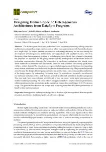
2 Proposed FPGA Interconnection Architecture In this section, we discuss the spatial information of Switch Box (SB) connections as well as the usage of longer segments and their impact on the FPGA interconnection architecture. For that purpose, we introduce a new method for deriving special maps, each of which describes the number, as well as the location (spatial) of used transistors within a SB. In order to build these maps, MCNC benchmarks, the EX-VPR tool [2] and a Virtex-like FPGA architecture [8] were used. The first step of the methodology is to find out the connectivity, the performance, the energy and the area requirements of MCNC benchmarks. For that purpose, a specific map (or 3-D curve) can be created for each design parameter which shows the parameter variation across the whole FPGA device. In particular, Fig. 1 shows the overall connectivity of the whole FPGA. It can be seen that the connectivity varies from point to point of FPGA. If we define a certain threshold of the connectivity value, and project the diagram to (X,Y) plane of FPGA, we create maps for connectivity requirements.
Designing Heterogeneous FPGAs with Multiple SBs
93
Considering connectivity threshold equal to 2, Fig. 1 shows the connectivity requirements of MCNC applications mapped into conventional FPGAs. The connectivity is defined as the total number of connections (i.e., “ON” pass-transistors) that take place into the SB. The number of distinct regions is based only to the designer requirements. By increasing the number of regions, the FPGA becomes more heterogeneous, as it is consisted by more regions. On the other hand, this increase leads to performance improvement for the device, due to the better routing resources utilization. As we can see from the exploration results, the number of the connections is gradually decreases from the centre of the map to the borders. The connectivity requirement for more tracks in the center of the device than the I/O boundary elements depends on the chosen placement and routing algorithm [2]. The introduction of connectivity map is very useful instrument to FPGA device designers to specify the interconnection requirements over each (x,y) point of FPGA device. Determining the “hot spots” locations of FPGA device, the designer can concentrate his/her efforts for efficient device optimization on certain regions only, but not on the whole device.
1,00
0,50
0,00
0,00-0,50
0,50-1,00
0,00-0,50
0,50-1,00
Fig. 1. Overall connectivity across the whole FPGA
The energy dissipation is critical issue of an FPGA design process. Since the power consumed in routing is more than 60% of total power of the FPGA device [9], the proposed technique aims at the minimization of this factor. For that purpose, we take into account the SB pass-transistors utilization in the various regions of FPGA map, shown in Fig. 1. Thus, in regions with smaller connectivity (i.e. fewer transistors) we can use appropriate type of SB with low-energy features. The connectivity degree of any (x,y) point of FPGA array is directly related with the energy consumption of (x,y) SB location, since less number of active SB connections means less energy consumption. Furthermore, as we increase the number of distinct SB regions, the designer can identify in more detailed manner the spatial distribution of energy consumption and therefore, he/she can choose the most appropriate SB for each region at the expense of the increased heterogeneity of FPGA features. On the other hand, increase of the SB regions has a penalty at the fabrication cost of the device. For this work we choose to use an FPGA array with two distinct SB areas. The second step of the proposed methodology is to determine the most appropriate wire length of a homogeneous FPGA, (i.e. considering the Subset, Wilton, and
94
K. Siozios et al.
Universal SBs). As it is mentioned, the selection of the optimal segment length is based on EDP criterion. Fig.2(a) gives the average variation of EDP curve for various segment lengths and the available SBs, where it can be seen that the segment L4 provides the minimal EDP. All the values at Fig. 2(a) and (b) are normalized to largest EDP value and they are the average values from all MCNC benchmarks. The horizontal axis represents the length of the routing wire segments, while the vertical one is the normalized value for a design parameter. It should be noted that the three curves (i.e. three SBs) are almost identical. Energy-Delay Product
Energy x Delay Product vs. Segment Length 1.00
1.0
0.90
0.9 0.8 Normalized Values
0.80 0.70 0.60 0.50 0.40
0.7 0.6 0.5 0.4 0.3
0.30
0.2
0.20
0.1 0.0
0.10
7
13 19 25 31 36 41 46 51 56 60 64 68 72 75 78 81 84 87 89 91 93 95 96 97 98 99 100
0.00 L1
L2
L4
L8
L16
L32
Segment Length
(a)
SUBSET_UNIVERSAL
SUBSET_WILTON
UNIVERSAL_SUBSET
UNIVERSAL_WILTON
WILTON_SUBSET
WILTON_UNIVERSAL
(b)
Fig. 2. (a) EDP for different segments, (b) EDP for different SBs
Employing the spatial information regarding with a SB location, the rest of the paragraph provides detailed data about the selection procedure of the optimal combination of SBs, considering the EDP criterion. This is the 3rd step of the proposed methodology. Assuming two FPGA regions each of which uses a different type of SB, we performed exploration for all possible values, of SB_ratio’s: SB _ ratio =
SB _ Type _ 1 (%) SB_ Type _ 2 (%)
(1)
where SB_Type_Region_1 and SB_Type_Region_2 denote the percentage of chosen SBs of Region_1 and Region_2. Fig. 2(b) shows the exploration results for EDP, assuming placement and routing to the smallest square FPGA with different ratios between the two distinct SBs. The values of the horizontal axis show the percentage of the first SB compared to the second one into the array. Moreover, having a combination {SB_Type_1} and {SB_Type_2}, the latter SB type is placed is an orthogonal located in the centre of FPGA, while the SB_Type_1 placed around the orthogonal up to I/O pads of FPGA. The exploration procedure was done by the EX-VPR tool, which can handle both the above three SBs and user-specified SBs [2]. We can deduct that the ratio 80%/20% of “Subset-Universal” combination, minimizes the EDP value. The Subset SB is assigned to Region_1, while Universal SB to Region_2 (center of FPGA). The aforementioned exploration procedure for the EDP can be also applied for the performance, the energy dissipation and the area requirements. Due to lack of space, we cannot provide the corresponding curves for these design parameters. However, we found that the proposed interconnection architecture provides the optimal results. It should be stressed that the primary goal of the proposed methodology is to prove that the usage of proper segment and combination of different properly-chosen SBs results into performance and energy consumption optimization.
Designing Heterogeneous FPGAs with Multiple SBs
95
3 Experimental Results The proposed interconnection architecture was implemented and tested by a number of MCNC benchmarks. The chosen MCNC benchmarks are the twenty largest ones, and they were placed and routed in an island-style FPGA array [6, 8], using the EX-VPR tool. All the benchmarks were mapped to the smallest FPGA array. Table 1 shows the results for delay and energy both for homogeneous architectures and the proposed one with multiple SBs and segment L4. In the homogeneous FPGAs, the whole device is composed by only one of the available SBs (Subset, Wilton or Universal). Since our primary goal is the design of both high performance and low energy FPGA architecture, we choose the optimal EDP value from the exploration results (Fig. 2(a) and (b)) for our exploration results. Table 1. Comparison results between the proposed FPGA architecture (with multiple-SBs & L4 segment) and single SB FPGA architectures in terms of delay and energy Benchmark alu4 apex2 apex4 bigkey clma des diffeq dsip elliptic ex5p ex1010 frisc misex3 pdc s298 s38417 s38584 seq spla tseg
Subset Delay x10-8 9.77 9.37 8.86 7.71 15.1 8.29 6.15 7.99 10.9 9.26 18.3 16.1 11.7 20.4 13.4 10.3 9.59 12.4 15.6 5.55
Energy x10-9 5.83 6.75 4.17 8.05 11.4 10.4 3.51 7.82 12.4 4.32 16.2 12.1 5.55 22.3 6.88 22.6 19.5 6.56 13.1 3.18
Wilton Delay x10-8 9.74 9.35 8.86 6.97 14.8 9.06 6.51 7.93 10.9 10.6 17.4 15.7 11.8 23.9 13.8 10.3 9.59 18.4 17.5 6.72
Energy x10-9 5.77 6.66 4.17 8.04 10.3 10.2 3.45 7.63 12.0 4.32 15.4 11.0 5.49 21.6 6.78 22.7 18.9 7.18 12.7 3.19
Universal Delay x10-8 10.9 13.1 10.3 6.26 14.9 8.65 6.03 7.93 12.3 9.55 26.4 15.8 10.1 15.2 13.4 9.91 9.59 8.87 19.0 6.03
Energy x10-9 5.84 6.94 4.24 7.87 10.5 10.2 3.43 7.61 12.4 4.27 17.1 11.2 5.28 18.7 6.92 22.5 19.0 6.10 13.1 3.15
Multiple SBs + L4 Architecture Delay Energy x10-8 x10⁻⁹ 4.29 5.36 5.24 6.66 4.51 4.10 3.10 7.34 9.30 7.65 4.56 9.83 5.46 3.55 3.66 6.75 7.15 12.8 4.31 4.52 8.16 15.6 9.89 8.14 4.08 4.66 7.58 18.2 8.24 6.95 5.80 23.4 4.70 19.1 4.43 6.28 6.54 11.4 4.82 2.96
It can be seen that the proposed method achieved significant reduction in EDP of average about 55%, reasonable gain in performance up to 52%, energy savings up to 8%, at the expense of increase channel width by 20%. The reported gains that reported results from the average value of partial gains of the proposed architecture to each single-SB architecture. We have to point out that during the exploration procedure we used the optimal channel width for all the benchmarks and interconnection devices. It should be stressed that we achieved to design a high performance FPGA, without any negative impact on energy, although high performance circuit means high switching activity and eventually increased energy.
96
K. Siozios et al.
4 Conclusions A novel FPGA interconnection methodology for high speed and energy efficient island-style FPGA architectures was presented. Using appropriately, the spatial information of various FPGA parameters, a new routing architecture with multiple-SBs and segment length L4 was designed. Using the minimal EDP value, the comparison results proved that heterogeneous FPGA platform outperforms with a conventional FPGA. More specifically, delay reduction up to 52% and energy savings up to 8% were achieved. Furthermore, the design of the new FPGA architecture is fully software-supported approach.
References 1. G. Varghese, J.M. Rabaey, “Low-Energy FPGAs- Architecture and Design”, Kluwer Academic Publishers, 2001. 2. K. Siozios, et al., “An Integrated Framework for Architecture Level Exploration of Reconfigurable Platform”, 15th Int. Conf. FPL 2005, pp 658-661, 26-28 Aug. 2005 3. S.Yang, “Logic Synthesis and Optimization Benchmarks, Version 3.0”, Tech.Report, Microelectronics Centre of North Carolina, 1991 4. K. Leijten-Nowak and Jef. L. van Meerbergen, “An FPGA Architecture with Enhanced Datapath Functionality”, FPGA’03, California, USA, pp. 195-204, Feb. 2003 5. V. Betz, J. Rose and A. Marquardt, “Architecture and CAD for Deep-Submicron FPGAs”, Kluwer Academic Publishers, 1999 6. http://vlsi.ee.duth.gr/amdrel 7. http://www.xilinx.com/products/silicon-solutions/fpgas/virtex/virtex4/overview 8. Deliverable Report D9: “Survey of existing fine-grain reconfigurable hardware platforms,” AMDREL project, available at http://vlsi.ee.duth.gr/amdrel/pdf/d9_final.pdf 9. Guy Lemieux and David Lewis, “Design of Interconnection Networks for Programmable Logic”, Kluwer Academic Publishers, 2004