Development and Application of Innovational Drop Impact Modeling Techniques Tong Yan Tee, Jing-en Luan, and Hun Shen Ng STMicroelectronics 629 Lorong 4/6 Toa Payoh, Singapore 319521. Phone: (65) 63507703 Fax: (65) 62598662 Email:
[email protected] Abstract Due to demand for short time-to-market, drop testing has become a bottleneck for semiconductor and telecommunication industry. Therefore, there is a need for a faster and cheaper solution, i.e. validated drop impact model, which is accurate, reliable, and enables understanding of physics-of-failure for design improvement. Currently, there has been increasing interest and effort by researchers on board level drop test studies by numerical modeling. Several different modeling methods have been developed to satisfy the requirements in package design analysis, product qualification, and impact life prediction. In this paper, for the first time, various advanced drop test modeling techniques developed are systematically introduced, integrated, compared, and recommended for various applications, consisting of analysis type (dynamic vs. static), loading method (free-fall vs. Input-G), and solver algorithm (explicit vs. implicit). Each combination of modeling techniques has its unique advantages, depending on applications. All the models are validated to show excellent first level correlation on the dynamic responses of PCB, second level correlation on the solder joint stress and failure mode, and third level correlation on impact life prediction. Dynamic model is required for accurate drop impact simulation, whereas static model is useful for quick design analysis and optimization. The freefall drop model can be applied to provide fundamental understanding of different drop test conditions, i.e. drop height, contact surface, drop block, felt layer on the impact pulse. Once the impact pulse has been established, the InputG method can be used as a standard “numerical drop test” to perform design analysis and optimization for product qualification. Implicit solver is an alternative to explicit solver, saving software cost by maintaining only one type of solver, but the technical challenge is greater.
telecommunication industry, which emphasizes on short timeto-market. Since board level drop test is a key qualification test for portable electronic products, it is becoming a topic of great interest by many researchers. Many works on drop test experiments [4-7] and simulation [8-10] were reported over the past few years. In order to have a good impact life prediction model with accurate design trend analysis, there are two prerequisites to be satisfied. One is a comprehensive drop impact modeling methodology; the other one is detailed experiment with well-controlled drop test results. Based on these two conditions with integration between simulation results and testing results, Tee et al. [11-33] reported a series of 23 publications over the past four years related to board level drop test. The studies consist of various novel drop impact modeling techniques with correlation to experiments [19, 21, 25-26], design analysis for enhanced drop impact performance of various advanced IC packages with both eutectic and lead-free solders [12-14, 29-30], as well as integrated numerical and experimental analysis under both board level drop test and thermal cycling test [16-17]. In this paper, for the first time, various advanced drop test modeling techniques developed are systematically introduced, integrated, compared, and recommended for various applications, consisting of analysis type (dynamic vs. static), loading method (free-fall vs. Input-G), and solver algorithm (explicit vs. implicit). Each combination of modeling techniques, e.g., dynamic/free-fall/explicit vs. dynamic/InputG/implicit, has its unique advantages, depending on applications.
2. Experimental Setup The simulation results from various models need to be validated by experimental results. Typical setup of board level drop tester [13] is shown in Figure 1. TFBGA packages (2x5 matrix) are mounted on test board (100x48x1.6mm), which is 1. Introduction The reliability performance of IC packages during drop connected to fixture (140x76.2x15mm) and drop table impact has become a great concern, due to increasing demand (210.5x210.5x70mm) with screws. Between board and and popularity of handheld or portable telecommunication fixture, 10mm standoff is added to allow PCB bending. The devices such as mobile phones and PDAs. The mechanical drop table or block is dropped from a certain height along the shock resulted from mishandling during transportation or two guiding rods, onto a rigid base covered with one layer of customer usage may cause solder joint failure, which leads to felt. The drop orientation is always in PCB horizontal malfunction of product. Board level drop test is convenient to direction with packages facing downwards (most severe characterize the solder joint performance. There are JEDEC direction [21]). A multi-channel real-time monitoring system standards [1-3] which provide guidelines to conduct board [15] as shown in Figure 2 is set-up to record down the input level drop test. However, the actual drop test is very acceleration of PCB, in-plane strains at PCB center, deflection expensive, time-consuming, and requires much more of PCB, and dynamic resistance of solder joints. The overall drop impact process involves a series of manpower in measurement and failure analysis. Therefore, energy transformation [19]. Firstly, the drop table falls down there is a need for a faster and cheaper solution, i.e. validated freely from a certain height, and its potential energy is drop test model, which can be a useful design enhancement converted into kinetic energy. Then, the drop table hits the and virtual qualification tool for the competitive strike surface and creates an impact pulse with certain G level 504 2005 Electronic Components and Technology Conference 0-7803-8906-9/05/$20.00 ©2005 IEEE
and pulse duration. Finally, the impact forces are transmitted through mounting screws to PCB, solder joints, and components. At the same time, the inertial force causes the PCB to bend and induce stresses in solder joints. At the instance of drop contact, the velocity of drop table is sharply reduced to zero and results in very high acceleration loading applied to four support screws of PCB assembly, while the PCB assembly is still traveling downwards. Therefore, the PCB bends down due to inertia force and then bends up with spring force. Consequently, it bends down and up cyclically till it is fully damped.
dependent on model size and element size. For example, solution time for a complex BGA module model with small element size can take up to 1-2 days with the latest computation capability. Therefore, static method for drop impact analysis is developed for quick first-order estimation or whenever dynamic model is unavailable due to technical or cost limitation. For example, it is known that the solder joint failure is mainly due to PCB cyclic bending after drop impact [19], and therefore, a deflection at PCB center (see Figure 3) can be applied to induce a bending load. This model induces excessively high stress on package at PCB center, and thus not suitable to study the effect of package position on board. Another simplified static model is shown in Figure 4. Equivalent forces are applied to the entire PCB subassembly uniformly such that the maximum PCB deflection and strain are the same as experimental measurements [18]. This static model is closer to the dynamic model at the instant of first maximum PCB bending after drop impact. The dynamic models are the main focus of this paper and will be elaborated in the remaining sections. Detailed results of comparison between dynamic and static models will be reported in future.
Figure 1. Setup of a typical board level drop tester Figure 3. Static model with deflection at PCB center
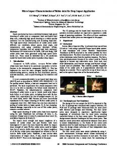
Figure 4. Static model with uniform bending forces 3.2 Loading Method (Free-fall vs. Input-G) By loading method, the drop impact process can be simulated in dynamic model as free-fall (conventional method) or fixed-end acceleration (novel Input-G method). Both methods are developed and validated to show excellent correlations with experiments (see Section 4). Figure 2. Multi-channel real-time monitoring system Two main types of dynamic drop impact models are developed by researchers, i.e. free-fall model (see Figure 5) 3. Modeling Techniques for Board Level Drop Test and Input-G model (see Figure 6). The free-fall method 3.1 Analysis Type (Dynamic vs. Static) simulates the actual drop testing process. The packages By analysis type, the drop impact models can be classified mounted on test board are connected to the drop block with into dynamic analysis and static analysis. The drop impact is screws and dropped from a certain height unto a contact physically a dynamic problem and dynamic analysis is surface. The impact pulse generated by the model is finenaturally required for accurate life prediction model. tuned by contact condition to match the experimental However, the solution time of dynamic analysis is highly requirements [22, 26]. As for the Input-G method [18-19], the 505 2005 Electronic Components and Technology Conference
impact pulse or input acceleration needs to be known beforehand and will be fixed or input to the connectors of PCB subassembly directly as a PCB boundary condition. Center (1/4 model) Screw
PCB Package
Drop Block Felt Contact surface
Figure 5. Dynamic model with free-fall method
G
G PCB G
G
Package Face Down
Figure 6. Dynamic Input-G model (explicit solver)
Here, a novel dynamic non-linear implicit algorithm with Input-G method is developed [25]. For solving transient dynamic problems, there exist explicit and implicit time integration schemes. The explicit time integration scheme applies the central difference approach in the time domain, which only works for a problem with diagonalized mass matrix. This scheme is particularly suitable for solving highly nonlinear problems as well as problems concerning wave propagations. Therefore, the explicit time integration scheme is always conditionally stable which desires a tiny time interval. On the other hand, the implicit time integration schemes, in general employing the Newmark algorithm, are usually unconditionally stable in solving linear elastic problems, which assures the feasibility of adopting a large time interval. Nevertheless, the implicit scheme is not computationally efficient for wave propagation problems and often diverges for highly nonlinear problems. The free-fall and Input-G dynamic models can be solved using both explicit and implicit solvers. However, the time interval and solution time may be different. Especially for large free-fall model, the solution time is almost unaffordable when implicit solver is adopted. That is why there is less effort put in this direction. However, it is still efficient for medium or small size model, and important for organizations without access to explicit solvers. A small model modification is needed for implicit Input-G method because the acceleration profile cannot be input directly into the implicit solver. Instead, the profile of timedependent displacement (see Figure 7) can be integrated from the impact pulse (to velocity profile first) and then directly applied to four support screws as boundary conditions of implicit Input-G model.
The free-fall method can be applied to provide fundamental understanding of different drop test conditions, i.e. drop height, contact surface, drop block, felt layer on the impact pulse. The free-fall model is useful to characterize a new drop tester to obtain the required impact pulse. It can also be used to predict the impact pulse for any testing conditions of any product at package, board or system level, as well as drop tester design variations when no testing result is available. Once the impact pulse has been established, the Input-G method can be used as a standard “numerical drop test” to perform design analysis and optimization for product qualification. Input-G method is more accurate and 4 times faster than free-fall method, and bypasses many technical difficulties in conventional free-fall method such as adjusting the parameters of contact surfaces, defining contact type, etc. Moreover, it is a convenient tool to study the effect of impact pulse variations on solder joint reliability.
Figure 7. Velocity and displacement of actual impact
3.3 Solver Algorithm (Explicit vs. Implicit) Most of the dynamic models utilize ANSYS/LS-DYNA or ABAQUS type of explicit solver, as the modeling effort and solution are usually much easier than the implicit solver. However, some companies are only equipped with implicitsolver type of finite element software for static structural or thermo-mechanical modeling. The implementation of dynamic model with implicit solver is known to be technically challenging.
4. Free-fall vs. Input-G Model In general, a validated drop impact model can be classified into three levels [19]: 1) good correlation of dynamic responses of PCB (system’s structural behavior), 2) good correlation of trend of solder joint stress/strain (qualitative), 3) good correlation of impact life (quantitative).
Velocity and Displacement 8
4
Velocity (m/s)
Displacement (mm)
6
3
5 4
2
3 2
1
Displacement (mm)
Velocity (m/s)
7
1 0 0
0.1
0.2
0.3
0.4
0 0.5
Time (ms)
506
2005 Electronic Components and Technology Conference
Due to lack of suitable sensor for measuring stress/strain in solder joint without affecting solder joint performance, correlation in the second level is difficult. However, the second level correlation can be a qualitative one which can help to understand failure mechanism and failure criteria. Quantitative impact life prediction requires sophisticated material model, and thus, correlation in the third level is very challenging. Therefore, good correlations of drop impact model with dynamic responses and failure modes are prerequisites to accurate solder joint reliability analysis and impact life prediction. Hence, such correlations are good tools to check the capability and efficiency of different drop impact models. 4.1 PCB Dynamic Responses (1st Level Correlation) The impact pulse generated by free-fall model is compared with the experimental value in Figure 8. The freefall model is able to fit the peak acceleration, Gm, and the pulse duration, T, closely. This can be adjusted using the drop height, contact surface, drop block material and felt layer/material [22, 26]. The shape of the impact pulse of the free-fall model is close but does not fully match the experimental impact pulse shape although the Gm and T may be equal. As shown in the Figure 8, the free-fall impact pulse (area = 978 G-ms) is larger than the experimental impact pulse (area = 756 G-ms). The lower experimental impact pulse can be due to effects of friction of guiding rods, different contact conditions and other unknown tester parameters. Impact Pulse
5000
Free-fall Model
Acceleration (G)
4000
Experimental
3000 Gm
2000 1000
T
0 -1000
0.2
0.4
0.6
0.8
1.0
PCB-Length Strain 6000 Experiment Free Fall Model
4000
Input-G Model
Microstrains
2000 0 0
1
2
3
4
5
-2000 -4000 -6000
Time (ms)
Figure 9. Comparison of PCB strain (length) 4.2 Solder Joint Stress and Failure Mode (2nd Level Correlation) The variation of stresses in the critical solder joint with impact time, including normal stress in PCB length direction (Sx), first principal stress (S1), vertical normal stress or peeling stress (Sz), shear stress (Sxz), and Von Mises stress (Seqv) for free-fall model are shown in Figure 10. Similar trend of results can be observed for Input-G model [19]. All the stresses vary cyclically under PCB vibration, corresponding to the measured dynamic strain of PCB. Among them, the peeling stress (Sz) has close amplitudes in positive and negative directions. It looks like an amplitudedeclining cyclic fatigue stress. Comparing the five stresses at the same critical point, the first principal stress follows the same pattern as the peeling stress, especially during the periods of positive peaks, indicating that the peeling stress is the dominant stress component. The Von Mises stress also mainly reflects the trend of the peeling stress. The remaining horizontal normal stresses and shear stresses are much lower in magnitude. Therefore, the solder joint peeling stress is critical during drop impact and can be used as a failure criteria for the purpose of design optimization [13, 19].
Time (ms)
Dynamic Stresses in the Critical Solder Joint
Figure 8. Numerical and experimental impact pulse
300 200 Stress (MPa)
The time-dependent dynamic strains in PCB length direction predicted by modeling for both free-fall and Input-G methods are shown in Figure 9. Simulation results obtained from both models correlate well with the experimental measurement. The amplitude and frequency of PCB vibration are almost similar between modeling and experiment. Other dynamic responses such as the output acceleration and velocity of PCB also show excellent correlation with experimental measurement [18]. Therefore, both free-fall and Input-G method are validated for drop test simulation. Excellent correlation in dynamic responses of PCB is a prerequisite to good correlation of solder joint reliability and drop impact life.
Sx Sz
100 0 0
1
2
3
4
-100
5
Sxz S1 Seqv
-200 -300
Time (ms)
Figure 10. Dynamic stresses during drop impact The peeling stress obtained from simulation is then superimposed with input acceleration, dynamic strain in PCB length direction and dynamic resistance obtained from experiments [19] as shown in Figure 11. Since strain gauge is
507
2005 Electronic Components and Technology Conference
mounted at the backside (non-component side) of PCB, the negative peak of strain means PCB bending downwards. The peeling stress has a positive peak and the solder joint is subjected to tensile stress when PCB bends down. At the same time, the dynamic resistance has a positive peak, indicating opening of crack. This further confirmed that the peeling stress is the dominant stress component affecting the solder joint reliability. The peeling stresses for both free-fall model and the Input-G model are compared in Figure 12. The stresses obtained by both models are closely matched to each other. Similar close trend can be obtained for all other stresses. Therefore, both the free-fall and the Input-G methods can be used confidently to predict the solder joint reliability with similar results. However, each method has its unique advantages in certain applications (see Section 6)
200
5000
Input Acceleration
Predicted Peeling stress at critical solder joint
150
4000
Dynamic Resistance
3000
100
2000
50
Figure 13. Critical solder ball and failure interface
1000
0 -50
Peeling Stress, Sz
G/microstrains /mV
Dynamic Responses
Stress(MPa)
The minimum requirement of a drop impact model is to have a good relative correlation between modeling and testing, so that the impact performance of other package designs can be evaluated qualitatively, i.e. better or worse. The reliability of solder joints during the drop impact is the main concern, as it affects the functionality of product.
0 0
2
4
6
8
10
12
14
-1000 -2000
-100
-3000
-150
Measured strain in Length Direction
-200
Sz
G level
Time (ms) Strain (Length)
Failure Analysis
-4000 -5000
Resistance
Figure 11. Dynamic responses during drop impact Figure 14. Failure analysis of critical solder joint
Solder Peeling Stress in Critical Solder Joint
Peeling Stress, Sz (MPa)
300
Free-Fall Model
4.3 Impact Life Prediction (3rd level correlation) Figure 15 shows that the solder peeling stresses obtained by Input-G method for lead-free (SnAgCu) BGA packages are closely related to actual impact lives measured [29]. A life prediction model is formulated using power law to relate the maximum peeling stress and mean impact life [12-14, 21, 29]
Input-G Model
200 100 0 0
1
2
3
4
5
-100
N mean = C1σ z
-200 -300
Time (ms)
Figure 12. Comparison of solder joint peeling stress The critical solder ball from free-fall model is observed at the outermost corner, with stress concentration along the solder/PCB pad interface (see Figure 13). Similar trend can be observed using the Input-G model [19]. The stress concentration predicted by modeling correlates well with the actual failure mode and the critical solder ball location/interface observed in the experiment by dye penetration test and cross-section (see Figure 14). Some BGA package designs may fail along solder/component pad interface [29].
C2
(1)
where Nmean is the mean impact life, σz is the maximum peeling stress (MPa) in the critical solder ball, C1 and C2 are the correlation constants. Mean impact life is a more consistent parameter compared with first-failure life, as the process and testing variation is minimized through averaging test data. Excellent correlation is achieved between mean impact lives predicted by modeling and measured by experiment (see Figure 16). The uncertainty of impact life prediction [29] is within ±20%, e.g. 50±10 drops for a typical BGA package, which is comparable with the accuracy of fatigue life prediction of solder joint under thermal cycling test.
508
2005 Electronic Components and Technology Conference
frequency components in the dynamic strain by modeling compared with the measured dynamic strain curve, which may be due to longer time step taken for saving computing time. There must be some compromise between accuracy and solution time. The result shows that it is good enough for comparison and a quick analysis with this novel method using implicit solver. Shorter time step may improve accuracy, however, the solution time may increase greatly. Selection of time step is dependent on the application. The results are also compared with the strain data predicted by explicit Input-G method. It shows that both solvers can predict the dynamic strain well.
Normalized Drop Normalized DropImpact ImpactLife Life
Drop Impact Life vs. Solder Joint Stress 3 2.5 2 1.5 1 0.5 0 0.8
0.9
1
1.1
1.2
1.3
1.4
Normalized Solder Joint Stress
Strain in Length Direction at PCB Center
Figure 15. Stress-life correlation for various BGA packages Strain (microstrain)
6000
D rop Impact Life Prediction 8
Normalized Predicted Life
7 6 5 4
Experiment
4000
Implicit Explicit
2000 0 -2000
0.0
1.0
2.0
3.0
4.0
5.0
6.0
-4000 -6000
3
Time (ms)
2
Figure 17. Comparison of strain (length) curves
1 0 0
1
2
3
4
5
6
7
8
Normalized Testing Life
Figure 16. Impact lives of modeling vs. experiment Similar life prediction models with good testing correlation were also established using free-fall method for QFN [12, 14], TFBGA [13, 21] and CSP [17] packages with eutectic solder. The good correlation of solder peeling stress and impact life is also recently observed in WLCSP packages and will be reported in future. Either Input-G or free-fall method can be applied for life prediction, as long as consistent modeling methodology is followed. With this validated model, a failure-free state can be determined, and drop test performance of new IC package or module design can be quantified, and further enhanced through modeling. This quantitative approach is different from traditional qualitative modeling, as it provides both accurate relative (design trend) and absolute (virtual qualification) impact life prediction. 5. Explicit Solver vs. Implicit Solver 5.1 Correlation of Dynamic Strains Input-G method is applied here to compare explicit and implicit solvers [25]. The time-dependent dynamic strain in PCB length direction predicted by modeling is shown in Figure 17. It correlates very well with the experimental measurement. The amplitude of PCB vibration decreases gradually with time. The trend of dynamic strain by modeling is the same as that by experiment. The period or frequency of vibration is almost the same. There are lacks of some high
5.2 Deflection of PCB The PCB bending effect is obvious from the dynamic strain and resistance curves [19]. Therefore, the PCB curvature is very important for evaluation of solder joint performance. Figure 18 shows the warpage distribution of PCB during the maximum downward bending. The PCB has much larger warpage difference in the length direction (about 3.5mm) than in the width direction (about 0.4mm). It implies that the outer row of solder balls in the PCB length direction warps more and has higher bending stress level. The relative displacement of any part of PCB against time to fixed screws can be obtained from modeling (see Figure 19). The deflections of PCB center predicted by both implicit and explicit Input-G models are close to the experiment data measured by high-speed camera. The validated model can be applied to determine the optimized package location on PCB for electronic manufacturers. It is almost impossible to characterize the whole-field PCB warpage distribution during drop impact using experimental method. (mm)
Figure 18. PCB maximum warpage distribution
509
2005 Electronic Components and Technology Conference
Deflection of PCB Center Experiment
7000
Implicit
2
Explicit
Peak Acceleration (Gm)
Deflection (mm)
3 1 0 -1 0
1
2
3
4
5
6
-2 -3 -4 Time (ms)
5500
0.70
5000
0.65 0.60
4500 Gm
0.55
T (ms)
0.50
3500
0.45
3000
0.40
2500
0.35 10
12
Figure 20. Effects of felt thickness on Gm and T
Pulse Duration (ms)
Peal Acceleration (G m)
Effect of Felt Thickness
4 6 8 Felt Thickness (mm)
4000 T ~ 0.54
3000
Gm
2000
Time (ms)
1000 0.5
1
1.5
2 2.5 3 3.5 4 H, Drop Height (m)
4.5
5
1 0.9 0.8 0.7 0.6 0.5 0.4 0.3 0.2 0.1 0 5.5
Figure 21. Effects of drop height on Gm and T Impact Pulse for Different JEDEC Levels 3500 3000 2500 Impact G
6.1 Free-fall Model The new board level drop tester usually needs to be characterized and calibrated to obtain the required impact pulse. The JEDEC standard recommends several test conditions, e.g., JEDEC Condition B (1500G, 0.5ms duration, half-sine pulse), as the input shock pulse to the PCB subassembly. However, the impact pulse is a function of various design parameters such as the drop block, felt material, contact surface materials and dimensions, as well as different testing conditions such as drop height The free-fall model can be applied to easily understand the effects of different design parameters on the peak acceleration and time duration of the impact pulse. For example, the effects of felt thickness and drop height on the peak acceleration (Gm) and pulse duration (T) are shown in Figures 20 and 21 respectively. Similarly, effects of other different design parameters on the impact pulse can also be obtained and was discussed in other works [23-24, 32]. The drop tester can then be calibrated to obtain the required impact pulse. Figure 22 shows the impact pulse obtained by free-fall model for different JEDEC test conditions.
2
5000
0
6. Applications of Drop Impact Models In the previous Sections 4 and 5, the free-fall model and the Input-G model with implicit and explicit solvers have been validated to show good first, second, and third level correlations. As such, all the dynamic models developed with various combinations of loading method and solver algorithm can be applied confidently for board level drop test simulation. In this section, the advantages of each modeling technique will be highlighted. The applications will determine the choice of modeling method.
0
6000
0
Figure 19. Relative displacement of PCB center
4000
Max G = 3050.7*H0.4493
Pulse Duration (ms)
Effect of Drop Height on G and T
4
H
G
2000 1500
B
F
A
E
1000 500
D
C
0 -500 0 -1000
1
2
3
4
Time (ms)
Figure 22. Impact pulses for different JEDEC drop test conditions 6.2 Input-G Model For Input-G model, impact pulse is directly applied at the PCB connectors as a boundary condition. As such, there is no need to model the fixture, drop block, felt and contact surface as compared to the free-fall model. This simplification reduces more than 1000 nodes/elements in the model. With simplified model, the solution time for Input-G method is about 4 times faster than free-fall method. As shown in Table 1, for the same time duration of 5ms, the solution of Input-G method only takes around 7.5 hours, compared to 28.5 hours for free-fall model. Table 1. Comparison of finite element models Drop Number of Solution Model Nodes/Elements Time (hrs) Free-fall 8987 / 6498 28.5 Input-G 7532 / 5322 7.5
As shown in Figure 8, the impact pulse obtained from free-fall model is close but not exactly matches the testing impact pulse. The lower experimental impact pulse is due to the effects of friction, different contact conditions, and other unknown tester parameters, which can be indirectly accounted for in the Input-G model by using the same impact pulse. Input-G method is a convenient tool to study the effects of different impact pulse parameters [23-24, 32]. The JEDEC 510 2005 Electronic Components and Technology Conference
standard [1] for board level drop test does not emphasize the effects and sensitivity of peak acceleration, duration, and shape of impact pulse, which should be key variables to affect solder joint reliability during drop impact. Loose control of these parameters usually results in scattering of drop test results. 6.3 Implicit Solver Implicit method shows its good capability in correlation with dynamic responses and solder joint reliability. The results obtained by implicit and explicit solver algorithms are very close. The implicit dynamic model is a significant costsaving to some companies as it does not require additional purchase of an explicit solver, but it can achieve the same level of modeling accuracy and solution time requirements. It may not be reasonable to directly compare implicit and explicit method in solution time. Because the solution time is strongly dependent on time step, model size, element size, and the method itself. Here, a rough comparison is done for the same model with different time steps for implicit and explicit Input-G method. The solution time for implicit method is about 30% longer than that for explicit method [25]. The solution time is acceptable, and it can be improved if the model is simplified and has no convergence problem. 6.4 Static Model The main advantage of static model is that it is much faster than dynamic model. Table 2 shows that for the same model size, the solution time of static model is 30 times faster than the dynamic model. More complicated material model (e.g. plasticity) can be applied with a short solution time. Static model is also useful for large geometry model with fine element size, which sometimes the solution may not be obtained at all using dynamic model if submodeling or massscaling modeling technique is not applied. Compromise sometimes may be required between time and accuracy. Table 2. Comparison between static and dynamic models Drop Number of Solution Model Nodes/Elements Time (hr) Dynamic 7532 / 5322 7.5 Static 7532 / 5322 0.25 The static model is more useful for applications in relative package/board design comparison, instead of absolute impact life prediction. Generally, static model is able to give the same trend of results as dynamic model for most of the design applications, especially when the bending is dominant. However, such static model is able to capture the effect of peak acceleration, but not the impact pulse duration effect. The time-dependent effect or shock wave propagation cannot be reflected in static model. Therefore, the static model may reflect the DNP (Distance to Neutral Point) effect and big changes in design variables. However, it may not capture the small and detailed design variables. Care must be taken when using such static model for marginal design case. In short, static model is more useful for quick design screening and first level optimization of large design matrix. Subsequently, selected key design variables from static model
can be further analyzed in the dynamic model. Dynamic model is more applicable for final design optimization as well as virtual qualification to determine the pass/failure status of a package on board under drop test. 7. Conclusions In this paper, various advanced drop test modeling techniques developed are systematically introduced, integrated, compared, and recommended for various applications, consisting of analysis type, loading method, and solver algorithm. Each combination of modeling techniques has its unique advantages, depending on applications. All the models are validated to show excellent first level correlation on the dynamic responses of PCB, second level correlation on the solder joint stress and failure mode, and third level correlation on the impact life prediction. Acknowledgments The authors would like to thank Dr. Carlo Cognetti and Mr. Kho Chek Lim from STMicroelectronics’ Corporate Package Development (CPD) for the management support in this project. References 1. JEDEC Standard JESD22-B111, Board Level Drop Test Method of Components for Handheld Electronic Products, 2003. 2. JEDEC Standard JESD22-B104-B, Mechanical Shock, 2001. 3. JEDEC Standard JESD22-B110, Subassembly Mechanical Shock, 2001. 4. Lim, C.T. and Low, Y.J., “Drop Impact Survey of Portable Electronic Products,” 53rd ECTC Conference Proc., 2003, pp. 113-120. 5. Sogo, T. and Hara, S., “Estimation of Fall Impact Strength for BGA Solder Joints,” ICEP Conference Proc., Japan, 2001, pp. 369-373. 6. Mishiro, K., “Effect of the Drop Impact on BGA/CSP Package Reliability,” Microelectronics Reliability Journal, 2002, Vol. 42(1), pp. 77-82. 7. Xie, D., Arra, M., Yi, S., and Rooney, D., “Solder Joint Behavior of Area Array Packages in Board Level Drop for Handheld Devices,” 53rd ECTC Conference Proc., 2003, pp. 130-135. 8. Wu, J., “Global and Local Coupling Analysis for Small Components in Drop Simulation,” 6th International LSDYNA Users Conference Proc., 2000, pp. 11:17 - 11:26. 9. Zhu, L., “Modeling Technique for Reliability Assessment of Portable Electronic Product Subjected to Drop Impact Loads,” 53rd ECTC Conference Proc., 2003, pp. 100-104. 10. Yeh, C. L. and Lai, Y. S., “Transition Analysis of Boardlevel Drop Response of Lead-free Chip-scale Package with Experimental Verifications,” 6th EPTC Conference Proc., Singapore, 2004, pp. 695-700. 11. Tee, T.Y., Ng, H.S., Lim, C.T., Pek, E., and Zhong, Z.W., “Application of Drop Test Simulation in Electronic Packaging,” 4th ASEAN ANSYS Conference Proc., Singapore, 2002.
511
2005 Electronic Components and Technology Conference
12. Tee, T.Y., Ng, H.S., Lim, C.T., Pek, E., and Zhong, Z.W., “Board Level Drop Test and Simulation of QFN Packages for Telecommunication Applications,” ICEP Conference Proc., Japan, 2003, pp. 221-226. 13. Tee, T.Y., Ng, H.S., Lim, C.T., Pek, E., and Zhong, Z.W., “Board Level Drop Test and Simulation of TFBGA Packages for Telecommunication Applications,” 53rd ECTC Conference Proc., 2003, pp. 121-129. 14. Tee, T.Y., Ng, H.S., Lim, C.T., Pek, E., and Zhong, Z.W., “Drop Test and Impact Life Prediction Model for QFN Packages,” Journal of Surface Mount Technology, 2003, Vol. 16(3), pp. 31-39. 15. Luan, J.E., Tee, T.Y., Pek, E., Lim, C.T., and Zhong, Z.W., “Modal Analysis and Dynamic Responses of Board Level Drop Test,” 5th EPTC Conference Proc., Singapore, 2003, pp. 233-243. 16. Tee, T.Y., Ng, H.S., and Zhong, Z.W., “Design for Enhanced Solder Joint Reliability of Integrated Passives Device under Board Level Drop Test and Thermal Cycling Test,” 5th EPTC Conference Proc., Singapore, 2003, pp. 210-216. 17. Tee, T.Y., Ng, H.S., Luan, J.E., Yap, D., Loh, K., Pek, E., Lim, C.T., and Zhong, Z.W., “Integrated Modeling and Testing of Fine-pitch CSP under Board Level Drop Test, Bend Test, and Thermal Cycling Test,” ICEP Conference Proc., Japan, 2004, pp. 35-40. 18. Tee, T.Y., Luan, J.E., Pek, E., Lim, C.T., and Zhong, Z.W., “Novel Numerical and Experimental Analysis of Dynamic Responses under Board Level Drop Test,” EuroSime Conference Proc., 2004, pp. 133-140. 19. Tee, T.Y., Luan, J.E., Pek, E., Lim, C.T., and Zhong, Z.W., “Advanced Experimental and Simulation Techniques for Analysis of Dynamic Responses during Drop Impact,” 54th ECTC Conference Proc., 2004, pp. 1088-1094. 20. Luan, J.E., Tee, T.Y., Chiu, A., Pek, E., Lim, C.T., and Zhong, Z.W., “Modal Analysis and Spectrum Analysis of PCB under Drop Impact,” SEMICON Advanced Packaging Technology Symposium, Singapore, 2004, pp. 97-105. 21. Tee, T.Y., Ng, H.S., Lim, C.T., Pek, E., and Zhong, Z.W., “Impact Life Prediction Modeling of TFBGA Packages under Board Level Drop Test,” Microelectronics Reliability Journal, 2004, Vol. 44(7), pp. 1131-1142. 22. Tee, T.Y., Ng, H.S., Luan, J.E., “Comparison of Free-fall vs. Input-G Drop Impact Models,” 6th EMAP Conference Proc., Malaysia, 2004, pp. 48-55.
23. Luan, J.E. and Tee, T.Y., “Effects of Impact Pulse on Dynamic Responses and Solder Joint Reliability of TFBGA Packages during Board Level Drop Test,” 6th EMAP Conference Proc., Malaysia, 2004, pp. 33-40. 24. Luan, J.E. and Tee, T.Y., “Analytical and Numerical Analysis of Impact Pulse Parameters on Consistency of Drop Impact Results,” 6th EPTC Conference Proc., Singapore, 2004, pp. 664-670. 25. Luan, J.E. and Tee, T.Y., “Novel Board Level Drop Test Simulation using Implicit Transient Analysis with Input-G Method,” 6th EPTC Conference Proc., Singapore, pp. 671677. 26. Ng, H.S., Tee, T.Y., and Luan, J.E., “Design for Standard Impact Pulses of Drop Tester using Dynamic Simulation,” 6th EPTC Conference Proc., Singapore, 2004, pp. 793799. 27. Ibe, E., Loh, K., Luan, J.E., and Tee, T.Y., “Underfill Effects on BGA Drop, Bend, and Thermal Cycle Tests,” Advanced Packaging Magazine, Feb. 2005, pp. 28-30. 28. Ng, F.K., Lim, C.T., Pek, E., Luan, J.E., and Tee, T.Y., “Effect of Dynamic Strain and Reworking Conditions on Failure of IC Packages on PCB under Drop Impact Test,” SEMICON Advanced Packaging Technology Symposium, Singapore, May 2005. 29. Luan, J.E., Tee, T.Y., Goh, K.Y., Ng, H.S., Baraton, X., Bronner, R., Sorrieul, M., Hussa, E., Reinikainen, T., Kujala, A., “Drop Impact Life Prediction Model for Leadfree BGA Packages and Modules”, EuroSime Conference Proc., Germany, Apr. 2005. 30. Luan, J.E., Tee, T.Y., Hussa, E., Reinikainen, T., Kujala, A., “Design for Drop Impact Reliability of Lead-free BGA Packages with Life Prediction”, ICEP Conference Proc., Japan, Apr. 2005. 31. Luan, J.E. and Tee, T.Y., “Integrated Modal Analysis and Spectrum Analysis of PCB Subassembly Dynamic Responses”, ICEP Conference Proc., Japan, Apr. 2005. 32. Luan, J.E. and Tee, T.Y., “Effect of Impact Pulse Parameters on Consistency of Board Level Drop Test and Dynamic Responses,” 55th ECTC Conference Proc., May 2005. 33. Tee, T.Y. Package and Board Level Reliability Modeling of Advanced CSP Packages for Telecommunication Applications, Ph.D. Thesis, Nanyang Technological University, Singapore, 2005, Chapters 7-8, pp. 126-184.
512
2005 Electronic Components and Technology Conference