1
DOE-ILP Based Simultaneous Power and Read Stability Optimization in Nano-CMOS SRAM Garima Thakral Computer Science and Engineering University of North Texas, Denton, TX 76203. Email:
[email protected] Saraju P. Mohanty Computer Science and Engineering University of North Texas, Denton, TX 76203. Email:
[email protected] Dhiraj K. Pradhan Department of Computer Science University of Bristol, Bristol, UK. Email:
[email protected] Elias Kougianos Electrical Engineering Technology University of North Texas, Denton, TX 76203. Email:
[email protected]
DRAFT
2
Abstract This paper presents a novel design flow and algorithms for simultaneous power-stability optimization of nano-CMOS static random access memory (SRAM) circuits. A 45nm single-ended seven transistor SRAM has been used as case study. The SRAM cell is subjected to a dual-VT h assignment based on a novel combined Design of Experiments and Integer Linear Programming (DOE-ILP) approach, resulting in 50.6% power reduction (including leakage) and 43.9% increase in the read static noise margin over the baseline design. The process variation analysis of the optimized cell is performed considering the variability effect in twelve device parameters. An 8 × 8 array is constructed to show the feasibility of the proposed SRAM cell. To the best of the authors’ knowledge, this is the first research reporting the use of DOE and ILP for optimization of conflicting targets of power and stability in SRAM.
Index Terms Nanoscale CMOS, Low-Power Design, Power Optimization, Static Random Access Memory (SRAM), Static Noise Margin (SNM)
I. I NTRODUCTION AND CONTRIBUTIONS A major part of systems-on-chip (SoC) is the memory subsystem. A typical state-of-the-art microprocessor die has a large portion devoted to on-chip memory [1]. High-performance, large-capacity SRAM is a crucial component in the memory hierarchy of modern digital systems. SRAM design requires balancing delay, area, and power dissipation. Memory accesses consume a substantial portion of the total power budget for many applications. Reducing power dissipation in SRAMs significantly improves power efficiency, reliability, and cost. SRAM stability has also become a major concern for nano-CMOS. It has become increasingly challenging to maintain an acceptable Static Noise Margin (SNM) in embedded SRAMs while scaling minimum feature sizes and supply voltages. SNM becomes worse during the read operation (read SNM) compared to the hold operation [2]. Thus, there is a pressing requirement to design SRAM where the read operation does not disturb the cell stability. The read SNM can serve as a figure of merit in stability evaluation of SRAM cells [3]. Process variation is a major concern at nanoscale CMOS technologies. Variations in device parameters translate into variations in SRAM circuit parameters, such as power and stability, which eventually lead to loss in parametric yield. Any asymmetry in the cells due to process variations makes them less stable. Under adverse operating conditions such cells may inadvertently flip and corrupt the data.
DRAFT
3
The novel contributions of this paper are: 1) A novel design flow for power and stability optimization in nanoscale CMOS SRAM is proposed. 2) A 45nm SRAM cell is subjected to the proposed methodology. 3) For simultaneous power and stability optimization of the SRAM, a novel combined Design of Experiments (DOE) - Integer Linear Programming (ILP) based algorithm is proposed that selects transistors for dual-VT h assignment. 4) Process variation analysis of the SRAM cell is presented to study the effect of twelve process parameters on its power and stability. 5) An 8 × 8 SRAM array is constructed and characterized using the power and stability optimized SRAM cell, to demonstrate its feasibility. The paper is organized as follows: Current related research is presented in section II. Section III discusses the proposed optimized design flow. The baseline design is discussed in section IV. Section V highlights the combined DOE-ILP simultaneous power and read stability optimization. Section VI studies the effect of variability in device parameters on the proposed SRAM cell stability and power, followed by conclusions and future research in section VII. II. P RIOR R ESEARCH IN SRAM D ESIGN A nine transistor SRAM cell with enhanced stability and reduced power is proposed in [2], [4]. A Schmitt-trigger based SRAM proposed in [5], providing better read stability and better write ability. A ten transistor, low-voltage SRAM cell with faster readout operation is proposed in [6]. A subthreshold approach has been used in [7]. The methodology in [8] analyzes the stability of an SRAM cell in the presence of random fluctuations in device parameters. [9], [10], [11], gives a method based on dual-VT h and dual-Tox assignment for low power while maintaining performance. A comparison of our research with existing literature is presented in Table I. It can be observed that we attain high stability and low power. The current archival journal paper is based on our shorter conference paper [14] and is expanding that work as follows: 1) A tabular comparison with existing literature is given in Table I to highlight the significance of our research. 2) The optimization methodologies are discussed in more detail in section III. 3) The Design of Experiments (DOE) part of the optimization is described in detail in section V, showing how the coefficients (half-effects) for the ILP models are obtained. DRAFT
4
TABLE I C OMPARATIVE P ERSPECTIVE WITH R ELATED P RIOR R ESEARCH
Research
Power
SNM
Optimization Approach
Liu [2]
31.9nW (leakage)
0.3V
Separate data access mechanism.
Kulkarni [5]
0.11µW
300mV
Schmitt Trigger.
Okumura [6]
–
0.36V
Column line assist scheme.
Agrawal [8]
–
150mV
Modeling based approach.
Singh [12]
11.53µW
305mV
Transmission gates are used as access transistors.
Liu [13]
12.5nW
222mV
Dynamic threshold voltage tuning.
This Paper
113.6nW
303.3mV
Combined DOE-ILP optimization.
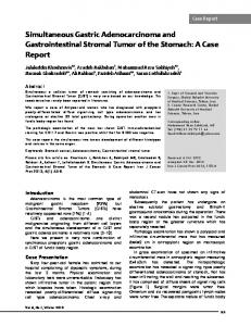
4) Pareto plots for the half-effects of transistors are presented. 5) Monte Carlo simulation results of power and SNM, and butterfly curves under process variation for approaches involving power minimization only (SP W R ) and SNM maximization only (SSN M ) are presented. III. P ROPOSED D ESIGN M ETHODOLOGY FOR P OWER AND S TABILITY O PTIMAL NANO -CMOS SRAM D ESIGN Fig. 1 shows the two approaches investigated in this paper. The input to each flow is a baseline cell, with minimum sized transistors. The figures of merit under consideration (power and SNM) are measured for the baseline design. The average power consumption and read SNM are considered in this paper. To reduce dissipation we propose a well-established process-level technique, dual threshold voltage. For the 45nm node, leakage is the major component of total power dissipation [16]. Its reduction through dual-VT h reduces total power. \ In approach 1 (Fig. 1(a)), predictive equations are formulated for power (f\ P W R ), and SNM (fSN M ). These equations, and the constraints are linear and each of the solution variables is restricted to be either 0 or 1. The linear objective function is optimized subjected to linear equality and linear inequality constraints. Thus, ILP is an optimal way to solve these predictive equations. The solution set for power minimization is called SP W R , and the solution set for SNM maximization is called SSN M . The overall objective set SOBJ is formulated as SP W R ∩ SSN M (∩ refers to the intersection of sets), where the transistors suitable for high and nominal VT h assignment are identified. Using the optimal configuration DRAFT
5
Baseline SRAM cell
Baseline SRAM cell
Measure baseline SNM, Power
Measure baseline SNM, Power
Using DOE, form predictive equations for f PWR , f SNM
Using DOE, form normalized predictive equations for f *PWR , f *SNM
Solve f PWR , f SNM using ILP: solution set S PWR , S SNM Form S OBJ = S PWR
Form f OBJ * =
f*PWR
( ) f*SNM
Solve f*OBJ using ILP Solution set: S OBJ*
S SNM
Assign high−VTh to transistors using S OBJ
Assign high−VTh to transistors using S OBJ*
Power, SNM optimal SRAM cell
Power, SNM optimal SRAM cell
Perform Process Variation Characterization of SRAM
Perform Process Variation Characterization of SRAM
(a) Optimization Flow - 1
(b) Optimization Flow - 2 Vdd
Vdd
BL
NMOS
WL PMOS 2
1
PMOS 4 Qb
Q
NMOS 3
NMOS
Write
6
Gnd PMOS
Gnd
NMOS 5
7
Write
(c) Topology of a 7-transistor SRAM cell
Fig. 1. Proposed design flow for simultaneous power and stability optimization of Nano-CMOS SRAM. A single-ended seven transistor cell [15]; load transistors - (2, 4), driver transistors - (3, 5), and access transistors - (1, 6 and 7).
DRAFT
6
the design is re-simulated. For nanoCMOS SRAM it is important to perform well under process variations, thus the statical variability is studied for twelve important parameters. \ In approach 2 (Fig. 1(b)), the normalized predictive equations for power (f\ P W R ∗), and SNM (fSN M ∗) \ \ \ are used. The objective function: f\ OBJ ∗ is formed as the ratio of fP W R ∗ and fSN M ∗. fOBJ ∗ is to be minimized using ILP, and leads to simultaneous power minimization (numerator) and SNM maximization (denominator). The solution set is called SOBJ , where the transistors suitable for high and nominal VT h assignment for achieving the objective are identified. The design is then re-simulated with this
configuration. The statical variability is studied subjected to twelve parameters. A seven transistor (7T) cell topology which is suitable for ultra-low voltage regimes and is tolerant to read failure is selected [15] as a case study. However, the proposed methodologies are also to other variants present in literature. IV. D ESIGN AND S IMULATION OF A 45nm CMOS 7T SRAM A. Cell Design Single-ended SRAMs are known for their low-power potential. The baseline cell is shown in Fig. 1(c) with initial (W/L) sizes. The cell is composed of a read and write access transistor (1), two crosscoupled inverters (transistors 2, 3, 4 and 5) and a transmission gate (transistors 6 and 7) which opens the feedback connection during the write operation. The cell operates on a single bit-line, instead of having two bit-lines as in standard six transistor cell. Both read and write are performed over the single bit-line. However, the word-line (WL) must be asserted high prior to write and read, as in the standard six transistor cell. When the cell is in hold mode, the WL is low and a strong feedback is provided to the cross-coupled inverters by the transmission gate. The power consumption (τP W R ) and SNM (τSN M ) of the baseline design are presented in Table II. τP W R and τSN M represent these values, because they are used as constraints in the optimization methodology. B. Power and Leakage Simulation and Measurement The total power of the circuit is defined as the summation of dynamic power, subthreshold leakage, and gate-oxide leakage. SRAM cells have a tendency to retain data for some duration of time as they cannot be shut off. So, minimizing leakage becomes a critical issue [7]. The total power is quantified as follows: Ptotal = Pdyn + Psub + Pgate ,
(1)
where Pdyn is the dynamic power, Psub is the subthreshold leakage, and Pgate is the gate-oxide leakage. DRAFT
7
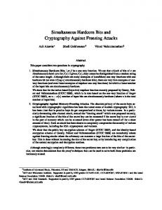
The current flow, which is manifested in leakage and power dissipation, in each device depends of the location the device and the operation. For accurate measurement of current (power) it is important that the currents are identified. Fig. 2 shows the paths for read and write operations. The dashed arrows are gate-oxide leakage, and subthreshold leakage is represented by dotted arrows. Solid arrows identify the dynamic current which flows when the transistor is ON. When the transistor is ON, it dissipates dynamic power along with the gate-oxide leakage [17]. When the transistor is OFF, it has gate-oxide leakage and subthreshold leakage. Current paths for write “1”, read “1”, write “0” and read “0” are shown in figures 2(a), 2(b), 2(c) and 2(d), respectively. C. Read Static Noise Margin (SNM) Simulation and Measurement SNM is defined as the maximum amount of noise that can be tolerated at the cell nodes just before flipping the states. A simulation based approach is used to measure SNM (Fig. 3(a)). Two DC voltage noise sources VN are placed in adverse direction to the input of each inverter of the cell to obtain the worst-case SNM. The sources are swept from 0 to Vdd until the cell voltages flip. A common graphical representation of SNM called butterfly curve is used during read access [10]. The SNM is defined as the length of the side of the largest square that can be embedded inside the lobes of the butterfly curve [3]. The power and SNM results are presented in Table II. TABLE II P OWER AND SNM R ESULTS FOR THE BASELINE SRAM
Parameters
Estimated Values
τP W R
203.6 nW
τSN M
170 mV
V. C OMBINED DOE-ILP O PTIMIZATION A LGORITHMS This section discusses the combined Design of Experiments (DOE)-Integer Linear Programming (ILP) algorithms. According to Algorithm 1, the baseline cell is taken as input along with the nominal and high VT h model files. Experimental analysis is then performed for the transistors of the cell using a 2-Level
DRAFT
8
Vdd
Vdd
Vdd
PMOS 2
’ON’
PMOS
dynamic current gate leakage current subthreshold leakage current
6
7
1
’1’ Q
NMOS 5 ’OFF’ Gnd
Write NMOS
NMOS 3 ’ON’ Gnd
’0’ Qb
PMOS 2 ’OFF’
NMOS 3 ’ON’ Gnd
PMOS 4 ’0’ Qb
’ON’
’OFF’
dynamic current gate leakage current subthreshold leakage current
’OFF’
Write
Vdd
Vdd
’ON’
Vdd
Vdd
WL’1’
1 ’0’ Q
’ON’
PMOS 4 ’1’ Qb
’OFF’
NMOS 3 Write
dynamic current gate leakage current subthreshold leakage current
PMOS
NMOS
’OFF’ Gnd
NMOS 5 ’ON’ Gnd
6
7
’0’ BL
PMOS 2 1 ’0’ Q
’ON’
’OFF’ Gnd
dynamic current gate leakage current subthreshold leakage current
Write
(c) Current path for write “0”
’1’ Qb
’OFF’
NMOS 3
’OFF’
’OFF’
PMOS 4
NMOS 5 ’ON’ Gnd
Write NMOS
PMOS 2
NMOS
NMOS
7
’ON’
(b) Current path for read “1”
WL’1’
Fig. 2.
6
Write
(a) Current path for write “1”
’0’ BL
NMOS 5 ’OFF’ Gnd
Write NMOS
’OFF’
’1’ BL
PMOS
’1’ Q
PMOS 4
PMOS
1
Vdd
WL’1’ NMOS
’1’ BL
NMOS
WL ’1’
6
7
’ON’
’ON’
Write
(d) Current path for read “0”
Current paths for the 7T SRAM cell during different read and write operations.
DRAFT
Vdd
Vdd
BL
NMOS
WL ’1’
1
PMOS 4
PMOS 2 Q
Qb
VN
VN
’1’
NMOS 3
NMOS 5
NMOS
6
PMOS
Write ’1’
Gnd
7
Gnd
Voltage on Qb−node (V)
9
Q−node Qb−node
0.6
0.5
0.4
0.3
0.2
0.1
0 0
0.1
Q−node Qb−node
0.5
0.4
0.3
0.2
0.1
0 0
0.1
0.2
0.3
0.4
0.4
0.5
0.6
0.7
0.5
0.6
0.7
(c) Butterfly curve for SP W R based cell.
Q−node Qb−node
0.6
0.5
0.4
0.3
0.2
0.1
0 0
0.1
0.2
0.3
0.4
0.5
0.6
0.7
Voltage on Q−node (V)
Voltage on Q−node (V)
Fig. 3.
0.3
(b) Read SNM for baseline cell.
Voltage on Qb−node (V)
Voltage on Qb−node (V)
(a) Simulation set-up.
0.6
0.2
Voltage on Q−node (V)
Write ’0’
(d) Butterfly curve for SSN M , SOBJ based cell.
Read SNM measurement in different configurations of SRAM cells.
Taguchi L8 array. The input factors are the 7 transistor VT h states, and the responses are the average \ power consumption (f\ P W R ) and SNM (fSN M ) of the cell. Each factor can take a high VT h (1) or a nominal VT h (0) state. Simulations are run for each experiment of the array and the values for both PWR and SNM are recorded. Then, the linear predictive equations are formulated. In Algorithm 2, the steps are the same as in algorithm 1. Here, however, the normalized (unitless) \ equations are formed for power (f\ P W R ∗)and SNM (fSN M ∗).
DRAFT
10
Algorithm 1 Approach 1 for simultaneous power and read stability optimization 1:
Input: Baseline PWR and SNM of the cell, Nominal and High VT h model files.
2:
Output: Optimized objective set SOBJ = [fP W R , fSN M ] cell with transistors identified for high VT h assignment.
3:
Setup experiment using L8 array, where the factors are VT h states, and the responses are average power consumption (fP W R ) and read SNM (fSN M ).
4:
for Each 1:8 experiments of L8 array do
5:
Run simulations.
6:
Record PWR and SNM.
7:
end for
8:
\ Form linear predictive equations: f\ P W R for power, fSN M for SNM.
9:
Solve f\ P W R using ILP. Solution set: SP W R .
10:
Solve f\ SN M using ILP. Solution set: SSN M .
11:
Form SOBJ = SP W R ∩ SSN M (intersection of SP W R and SSN M ).
12:
Assign high VT h based on SOBJ .
13:
Re-simulate SRAM cell to obtain power and SNM.
The half-effects are given by:
[ where
∆(n) 2
∆(n) = 2
]
(
avg(1) − avg(0) 2
) ,
(2)
is the half-effect of nth transistor, avg(1) is the average value of power when transistor
n is in high-VT h state, and avg(0) is the average value of power when transistor n is in nominal VT h
\ state. Figs. 4(a) and 4(b) show the pareto plots of the half-effects of the transistors for f\ P W R and fSN M , respectively. Predictive equations are then obtained as follows: ) 7 ( ∑ ∆(n) ˆ ¯ × xn , (3) f =f+ 2 n=1 [ ] where fˆ is the response, f¯ is the average, ∆(n) is the half effect of the nth transistor, and xn is the 2 VT h state of the nth transistor.
DRAFT
11
Algorithm 2 Approach 2 for simultaneous power and read stability optimization 1:
Input: Baseline PWR and SNM of the cell, Nominal and High VT h model files.
2:
Output: Optimized objective set SOBJ = [fP W R , fSN M ] cell with transistors identified for high VT h assignment.
3:
Setup experiment using L8 array, where the factors are VT h states, and the responses are average power consumption (fP W R ) and read SNM (fSN M ).
4:
for Each 1:8 experiments of L8 array do
5:
Run simulations.
6:
Record PWR and SNM.
7:
end for
8:
\ Form normalized predictive equations: f\ P W R ∗ for power, fSN M ∗ for SNM.
9:
Form fOBJ ∗ =
f\ P W R∗ . f\ SN M ∗
10:
Solve f\ OBJ ∗ using ILP. Solution set: SOBJ .
11:
Assign high VT h to transistors based on SOBJ .
12:
Re-simulate SRAM cell to obtain power and SNM.
A. Solution for power minimization: SP W R The predictive equation for average power consumption is: f\ P W R (nW ) = 118.2075 − 5.975 × x1 − 28.955 × x2 − 23.1625 × x3 − 10.995 × x4 − 10.6375 × x5 − 12.1425 × x6 + 6.475 × x7 .
(4)
Where, xi represents the VT h of transistor i (Fig. 1(c)). The ILP formulation is: min f\ PWR s.t.
0 ≤ x1 ≤ 1, 0 ≤ x2 ≤ 1, 0 ≤ x3 ≤ 1, 0 ≤ x4 ≤ 1, 0 ≤ x5 ≤ 1, 0 ≤ x6 ≤ 1, 0 ≤ x7 ≤ 1, fSN M > τSN M .
where the constraints ‘1’ and ‘0’ represent coded values for high VT h and nominal VT h states and τSN M is the SNM of the baseline design. The optimal solution is: SP W R = [x1 = 1, x2 = 1, x3 = 1, x4 = 1, x5 = 1, x6 = 1, x7 = 0]. Fig. 5(a) shows the configuration for minimum power consumption, with the
high VT h transistors circled. The power consumption is 26.34 nW with an SNM of 231.9 mV (Table III). Fig. 3(c) shows the butterfly curve obtained. DRAFT
30
20
10
0
2
3
6
4
5
7
1
Half Effect |∆/2| for SNM (mV)
Half Effect |∆/2|for PWR(nW)
12
50
0
Transistor Number (a) Power
Fig. 4.
2
3
1
5
7
6
4
Transistor Number (b) Read SNM
Pareto plot for power and SNM of the SRAM cell.
B. Solution for SNM maximization: SSN M The predictive equation for the read SNM is: f\ SN M (mV ) = 156.675 − 44.025 × x1 + 58.725 × x2 − 53.925 × x3 − 6.425 × x4 + 32.575 × x5 + 19.375 × x6 − 19.625 × x7 ,
(5)
The ILP formulation is: max f\ SN M s.t.
0 ≤ x1 ≤ 1, 0 ≤ x2 ≤ 1, 0 ≤ x3 ≤ 1, 0 ≤ x4 ≤ 1, 0 ≤ x5 ≤ 1, 0 ≤ x6 ≤ 1, 0 ≤ x7 ≤ 1, fP W R < τP W R .
where τP W R is the power consumption of the baseline design. The optimal solution is obtained as follows: SSN M = [x1 = 0, x2 = 1, x3 = 0, x4 = 0, x5 = 1, x6 = 1, x7 = 0]. Fig. 5(b) shows the SRAM configuration
for SSN M , with the high VT h transistors circled. The power consumption is 113.6 nW with an SNM of 303.3 mV (Table III). Fig. 3(d) shows the butterfly curve.
C. Solution for power minimization and SNM maximization: SOBJ 1) Approach 1: The overall objective set SOBJ for simultaneous optimization of power and SNM is to achieve low power and high stability. Hence a solution between SP W R and SSN M is explored. In DRAFT
13
approach 1, the following solution set is formed: SOBJ = SP W R ∩ SSN M ,
(6)
where ∩ is the intersection of two solution sets SP W R and SSN M . Equation 6 is derived for the set domain where the AND operation in the logic domain translates to intersection in the set domain. The constraints are same as the individual ILP formulations. The ILP solver results in the following solution: SOBJ = [x1 = 0, x2 = 1, x3 = 0, x4 = 0, x5 = 1, x6 = 1, x7 = 0]. Fig. 5(c) shows the configuration for
approach 1, with the high VT h transistors circled. The power consumption is 113.6 nW with an SNM of 303.3 mV (Table III). Fig. 3(d) shows the butterfly curve. \ \ 2) Approach 2: The normalized forms of f\ P W R and fSN M are used, denoting them as fP W R ∗ and f\ SN M ∗. These equations have been normalized by division of each value of the data by the maximum
value of data. The following normalized predictive equations are obtained: f\ P W R ∗ = 0.58 − 0.03 × x1 − 0.14 × x2 − 0.11 × x3 − 0.05 × x4 − 0.05 × x5 − 0.06 × x6 + 0.03 × x7 ,
(7)
and f\ SN M ∗ = 0.52 − 0.15 × x1 + 0.19 × x2 − 0.18 × x3 − 0.02 × x4 + 0.11 × x5 + 0.06 × x6 − 0.06 × x7 ,
(8)
The objective function is: f\ OBJ ∗ =
f\ P W R∗ , f\ SN M ∗
= 0.18 × x3 − 0.02 × x4 + 0.11 × x5 + 0.06 × x6 − 0.06 × x7 ,
(9)
\ The aim is to minimize f\ OBJ ∗, where the numerator (fP W R ∗) would be minimized, and the denominator (f\ SN M ∗) would be maximized. The ILP formulation is: min f\ OBJ ∗ s.t.
0 ≤ x1 ≤ 1, 0 ≤ x2 ≤ 1, 0 ≤ x3 ≤ 1, 0 ≤ x4 ≤ 1, 0 ≤ x5 ≤ 1, 0 ≤ x6 ≤ 1, 0 ≤ x7 ≤ 1, fP W R < τP W R , fSN M > τSN M . DRAFT
14
W=45nm L=45nm 2
1
0.22V BL
4
Vdd
−0.4V
WL
W=45nm L=45nm Qb
Q
Vdd
−0.4V
W=45nm L=45nm
W=45nm L=45nm
BL
Vdd
−0.4V
WL
W=45nm L=45nm 2
1
W=45nm L=45nm 4
Qb
Q
Vdd
−0.22V
0.4V 3 W=45nm L=45nm
5 W=45nm 0.4V L=45nm Write
Write
0.22V
W=45nm W=45nm L=45nm L=45nm
0.4V
−0.22V
5 W=45nm 0.4V L=45nm
6
0.4V
7
−0.22V
(a) Configuration for SP W R
−0.22V
W=45nm L=45nm 2
1
Vdd
W=45nm L=45nm 4
Qb
Q 3 W=45nm L=45nm
5 W=45nm 0.4V L=45nm
−0.22V
W=45nm W=45nm L=45nm L=45nm
Write
0.22V
7
−0.4V
WL 0.22V BL
Vdd
W=45nm L=45nm 2
1
Vdd
W=45nm L=45nm 4
Qb
Q 3 W=45nm L=45nm
5 W=45nm 0.4V L=45nm Write
0.22V
6
−0.22V
W=45nm W=45nm L=45nm L=45nm
BL
W=45nm L=45nm
0.22V
Vdd
0.4V
(b) Configuration for SSN M
W=45nm L=45nm
−0.4V
6
Write
Write
WL
W=45nm W=45nm L=45nm L=45nm
3 W=45nm L=45nm
0.4V
7
6
0.4V
7
−0.4V Write
(c) Configuration for SOBJ : Approach 1
Write
(d) Configuration for SOBJ : Approach 2
Fig. 5. Dual VT h configurations of 7T SRAM cell according to SP W R , SSN M and SOBJ with their threshold voltages marked on the side. The high VT h (VT hn = 0.4V , VT hp = −0.4V ) transistors are circled and the remaining transistors are nominal VT h (VT hn = 0.22V , VT hp = −0.22V ).
DRAFT
15
Solving the ILP problem, the optimal solution is: SOBJ = [x1 = 0, x2 = 1, x3 = 0, x4 = 0, x5 = 1, x6 = 1, x7 = 1]. Figure 5(d) shows the configuration for approach 2, with the high VT h transistors circled. The power consumption is 100.5 nW with an SNM of 303.3 mV (Table III). Fig. 3(d) shows the butterfly curve. TABLE III O PTIMIZATION R ESULTS FOR DIFFERENT OBJECTIVES
Optimization
Parameter
Value
Change
SP W R
PSRAM
26.34 nW
87.1% decrease
SNM
231.9 mV
26.7% increase
PSRAM
113.6 nW
44.2% decrease
SNM
303.3 mV
43.9% increase
SOBJ
PSRAM
113.6 nW
44.2% decrease
Approach 1
SNM
303.3 mV
43.9% increase
SOBJ
PSRAM
100.5 nW
50.6% decrease
Approach 2
SNM
303.3 mV
43.9% increase
SSN M
Fig. 6 shows the comparison of baseline and optimized cell power and read SNM for various values of Vdd . Both power and SNM increase with supply voltage. For Vdd = 0.7V the power dissipation is reduced by 44.2% and SNM has increased by 43.9% using approach 1, and the power dissipation is
SNM (mV)
reduced by 50.6% and SNM is increased by 43.9% using approach 2. 300 200
Avg. Power (nW)
Increase in SNM
100 0 0.4
Fig. 6.
SNM Baseline SNM Optimized
0.45
0.5
0.55
0.6
0.65
0.7
Supply Voltage (VDD) 250 200 150 100 50 0.4
Decrease in Power
Power Baseline Power Optimized
0.45
0.5
0.55
0.6
0.65
0.7
Supply Voltage (VDD)
Power and SNM comparison of optimal and baseline SRAM.
DRAFT
16
WL0
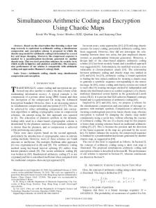
For an 8 × 8 array using the optimized cells (Fig. 7), the average power consumption is 4.5 µW .
PMOS
PMOS
Write0
NMOS
BL0
Fig. 7.
PMOS
PMOS
PMOS
PMOS
NMOS
NMOS
NMOS
NMOS
NMOS
NMOS
NMOS
NMOS
NMOS
NMOS
NMOS
PMOS
PMOS
PMOS
CELL0
BL1
CELL1
BL7
CELL7
Schematic representation of one row of the 8 × 8 array constructed using optimized 7T cells.
VI. S TATISTICAL VARIABILITY A NALYSIS OF THE SRAM Threshold voltage variation is strongly related to device geometry and doping profile. We selected twelve process parameters for process variation: (1,2) Toxn,oxp : NMOS, PMOS gate oxide thickness (nm), (3,4) Lna,pa : NMOS, PMOS access transistor channel length (nm), (5,6) Wna,pa : NMOS, PMOS access transistor channel width (nm), (7,8) Lnd , Wnd : NMOS driver transistor channel length, width (nm), (9,10) Lpl , Wpl : PMOS load transistor channel length, width (nm), (11,12) Nchn,chp : NMOS, PMOS channel doping concentration (cm−3 ), Some of the parameters are correlated; this is taken into consideration during simulation for realistic study. The SNM is exhaustively evaluated through 1000 Monte Carlo simulations.Figs. 8(a), 8(d), 8(g), 8(j) show the effect of process variations on the butterfly curve with SP W R , SSN M and SOBJ based configurations, respectively. Figs. 8(b), 8(e), 8(h), 8(k) show the distributions for “SNM High” and “SNM Low” extracted from the Monte Carlo simulations with SP W R , SSN M and SOBJ based configurations. “SNM Low” is treated as the actual SNM. Table IV shows the corresponding statistical data. Figs. 8(c), 8(f), 8(i), 8(l) show the distribution of average power. It follows a lognormal nature. VII. S UMMARY, C ONCLUSIONS AND F UTURE R ESEARCH A methodology is presented for simultaneous optimization of SRAM cell power and read stability. A 45nm single-ended 7T cell is used as case study, leading to 50.6% power reduction (including leakage)
and 43.9% increase in read stability (read SNM). A novel DOE-ILP approach has been used for power
DRAFT
17
400
450
SNM Low SNM High
400
350
300
Frequency
Number of Runs
350
250 200 150
200
150
50
0.1
0.2
0.3
0.4
0 −7.8
0.5
SRAM Static Noise Margin (V)
−7.55
−7.3
SRAM Average Power (Log scale)
(a) Butterfly Curve for
(b) SNM Distribution
(c) Power Distribution
(d) Butterfly Curve for
SP W R
for SP W R
for SP W R
SSN M
400
SNM Low SNM High
350
350
300
Frequency
300
250 200 150
200 150 100
50
50 0.2
0.3
0.4
0.5
0.6
SRAM Static Noise Margin (V)
0
SNM Low SNM High
350
250
100
0 0.1
400
µ = 147.73nW σ = 101.4nW
Number of Runs
400
300 250 200 150 100 50
−7.4
−7.2
−7
−6.8
−6.6
0 0.1
−6.4
0.2
0.3
0.4
0.5
0.6
SRAM Static Noise Margin (V)
SRAM Average Power (Log scale)
(e) SNM Distribution
(f) Power Distribution
(g) Butterfly Curve for
(h) SNM Distribution
for SSN M
for SSN M
SOBJ : Approach 1
for SOBJ : Approach 1
400
300
400
µ = 147.73nW σ = 101.4nW
250 200 150 100
−7.4
−7.2
−7
−6.8
−6.6
300
250 200 150 100
0 0.1
−6.4
µ = 135.24 nW σ = 101.85 nW
250
200
150
100
50
0.2
0.3
0.4
0.5
0.6
SRAM Static Noise Margin (V)
SRAM Average Power (Log scale)
350
300
50
50 0
400
SNM Low SNM High
350
Number of Runs
350
Frequency
Number of Runs
250
100
0 0
Frequency
300
100 50
Fig. 8.
µ = 28.91 nW σ = 8.26 nW
0
−7.5
−7
−6.5
SRAM Average Power (Log scale)
(i) Power Distribution
(j) Butterfly Curve for
(k) SNM Distribution
(l) Power Distribution
for SOBJ : Approach 1
SOBJ : Approach 2
for SOBJ : Approach 2
for SOBJ : Approach 2
Process variation study for SP W R , SSN M and SOBJ based configurations using Monte Carlo simulations.
minimization and read SNM maximization. The effect of process variation of twelve process parameters on the proposed cell is evaluated, and it is found to be process variation tolerant. An 8 × 8 array has been constructed using the optimized cell and data for power consumption is presented. A fair comparison of the proposed methodology with prior research is difficult. The proposed and existing research differ in terms of technology node, topology, and array size. However, a broad compar-
DRAFT
18
TABLE IV S TATISTICAL P ROCESS VARIATION E FFECTS ON SRAM P OWER AND SNM
Optimization
Parameter
µ
σ
SP W R
PSRAM
28.91nW
8.26nW
SNM
180mV
30mV
PSRAM
147.73nW
101.4nW
SNM
295mV
28mV
PSRAM
147.73nW
101.4nW
SNM
295mV
28mV
PSRAM
135.24nW
101.85nW
SNM
295mV
28mV
SSN M
SOBJ : Approach 1
SOBJ : Approach 2
ative perspective is presented with some closely related research [9], [11], [10] which does not account for dynamic current in optimization and only leakage minimization is measured whereas the current paper taken into account all components like dynamic, subthreshold, gate-oxide leakages. In [9], [11], a combined dual-VT h and dual-Tox assignment is used where the leakage power reduction is 53.5% and SNM increase is 43.8%. However, the current methodology which considers only dual-VT h (this is significant in terms of manufacturing cost) has resulted in power reduction (accounting all components) of 50.6% and increase in read SNM as 43.9%. Future research will involve array-level optimization of SRAM where mismatch and process variation will be considered as part of the design flow. Also, thermal effects will be incorporated. Simultaneous PVT optimal SRAM design for sub-45nm technology will be performed. Also, to make the optimization methodology more practical, transistor size will be included along with VT h state for each transistor in the search space. ACKNOWLEDGMENT This research is supported in part by NSF award number CCF-0702361 and CNS-0854182. This archival journal paper is based on the shorter conference paper [14]. The authors would like to acknowledge Dhruva Ghai for his inputs. R EFERENCES [1] N. Yoshinobu and et al., “Review and future prospects of low voltage RAM circuits,” IBM journal of research and development, vol. 47, no. 5/6, pp. 525–552, 2003. DRAFT
19
[2] Z. Liu and V. Kursun, “Characterization of a novel nine-transistor sram cell,” IEEE Transactions on VLSI Systems, vol. 16, no. 4, p. 488492, April 2008. [3] E. Seevinck and et. al., “Static noise margin analysis of MOS SRAM cells,” IEEE Journal of Solid-State Circuits, vol. 22, no. 5, p. 748754, October 1987. [4] S. Lin, Y. B. Kim, and F. Lombardi, “A low leakage 9t sram cell for ultra-low power operation,” in Proceedings of the ACM Great Lakes symposium on VLSI, 2008, pp. 123–126. [5] J. P. Kulkani, K. Kim, S. P. Park, and K. Roy, “Process Variation Tolerant SRAM Array for Ultra Low Voltage Applications,” in Proceedings of the Design Automation Conference, 2008, pp. 108–113. [6] S. Okumura and et al., “A 0.56-V 128kb 10T SRAM Using Column Line Assist (CLA) Scheme,” in Proceedings of the International Symposium on Quality Electronic Design, 2009, pp. 659–663. [7] N. Verma and A. P. Chandrakasan, “A 256 kb 65 nm 8T Subthreshold SRAM Employing Sense-Amplifier Redundancy,” IEEE Journal of Solid-State Circuits, vol. 43, no. 1, pp. 141–149, January 2008. [8] K. Agarwal and S. Nassif, “Statistical Analysis of SRAM Cell Stability,” in Proceedings of the Design Automation Conference, 2006, pp. 57–62. [9] B. Amelifard, F. Fallah, and M. Pedram, “Reducing the Sub-threshold and Gate-tunneling Leakage of SRAM Cells using Dual-Vt and Dual-Tox Assignment,” in Proceedings of the Design Automation and Test in Europe, 2006, pp. 1–6. [10] J. Lee and A. Davoodi, “Comparison of Dual-Vt Configurations of SRAM Cell Considering Process-Induced Vt Variations,” in Proceedings of the International Symposium on Circuits and Systems, 2007, pp. 3018–3021. [11] B. Amelifard, F. Fallah, and M. Pedram, “Leakage Minimization of SRAM Cells in a Dual-Vt and Dual-Tox Technology,” IEEE Transactions of VLSI Systems, vol. 16, no. 7, pp. 851–860, 2008. [12] J. Singh, J. Mathew, S. P. Mohanty, and D. K. Pradhan, “A Nano-CMOS Process Variation Induced Read Failure Tolerant SRAM Cell,” in Proceedings of the International Symposium on Circuits and Systems, 2008, pp. 3334–3337. [13] Z. Liu, S. Tawfik, and K. V, “Statistical Data Stability and Leakage Evaluation of FinFET SRAM Cells with Dynamic Threshold Voltage Tuning under Process Parameter Fluctuations,” in Proceedings of the Quality Electronic Design, 2008. ISQED 2008. 9th International Symposium, 2008, pp. 305–310. [14] G. Thakral, S. P. Mohanty, D. Ghai, and D. K. Pradhan, “A Combined DOE-ILP Based Power and Read Stability Optimization in Nano-CMOS SRAM,” in Proceedings of the 23rd IEEE International Conference on VLSI Design (ICVD), 2010, pp. 45–50. [15] J. Singh, J. Mathew, D. K. Pradhan, and S. P. Mohanty, “A Subthreshold Single Ended I/O SRAM Cell Design for Nanometer CMOS Technologies,” in Proceedings of the International SOC Conference, 2008, pp. 243–246. [16] S. P. Mohanty and E. Kougianos, “Simultaneous Power Fluctuation and Average Power Minimization during Nano-CMOS Behavioural Synthesis,” in Proceedings of the 20th IEEE International Conference on VLSI Design, 2007, pp. 577–582. [17] E. Kougianos and S. P. Mohanty, “Metrics to Quantify Steady and Transient Gate Leakage in Nanoscale Transistors: NMOS Vs PMOS Perspective,” in Proceedings of the 20th IEEE International Conference on VLSI Design (VLSID), 2007, pp. 195–200.
DRAFT