Mike Tien-Chien Lee, Yu-Chin Hsuy, Ben Chen , and Masahiro Fujita. Fujitsu Laboratories of America ... Kawasaki 211, Japan. Abstract: This paper presents our ...
Domain-Speci c High-Level Modeling and Synthesis for ATM Switch Design Using VHDL Mike Tien-Chien Lee, Yu-Chin Hsuy , Ben Chen� , and Masahiro Fujita �Fujitsu Ltd. Fujitsu Laboratories of America y Dept. of Computer Science 3350 Scott Blvd., Bldg. #34 Univ. of California 1015, Kamikodanaka Nakahar-Ku Santa Clara, CA 95054, USA Riverside, CA 92521, USA Kawasaki 211, Japan
Abstract:
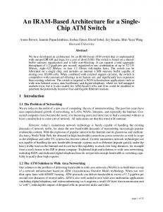
ing/transferring high-speed packets and a complex control path for managing concurrent events in the system. Therefore, it is essential to exploit such architectural features to develop a good behavior model for synthesis, and incorporate these features into high-level synthesis, which can hence focus on a more speci c design space to produce high-quality architectures e�ciently. This paper reports our experience on VHDL modeling and synthesis of Fujitsu ATM switch using high-level synthesis methodology. We propose a high-level design methodology by developing a VHDL behavior modeling scheme suitable for the target ATM switch design, and prototyping a domain-speci c high-level synthesis compiler to synthesize the developed behavior model. Important VHDL modeling techniques for the ATM switch, such as system partitioning for e�cient synthesis, clock 1 Introduction conversion for multiple clockings, process communiATM (Asynchronous Transfer Mode) has been con- rate cation using appropriate protocols, and arbitrator prosidered by telecommunication industry the ultimate so- cesses to sequence concurrent signal updates, are dislution to the networking requirement for Broadband cussed in the paper. ISDN [1]. Among the major components of ATM hardA VHDL high-level synthesis system, called MEBS, ware, the core technology is the ATM switches, which is proposed for domain-speci c ATM switch syntheare capable of sending ATM packets from one end to sis. MEBS synthesizes the developed mixed-level the other in a communication network when connected VHDL model down to a gate-level netlist by performin a speci c topology. Due to its short product life cycle ing scheduling, allocation, and RTL synthesis. It proand various demands from di�erent market segments, vides several features which are very useful for our current gate or lower level design methodology can no ATM switch synthesis, such as design space exploration longer satisfy the stringent time-to-market requirement for multiple processes, module function implementation for ATM switch design. It has become necessary to ex- for subprograms, and high-level incremental synthesis. ploit a higher-level methodology which can specify and Experimental results show that given the design consynthesize the design from an abstraction level higher straints, the proposed high-level design methodology is than logic gates. High-level synthesis [2], which takes able to produce a gate-level implementationusing MEBS an algorithmic speci cation as input and automatically with about 15% area reduction in shorter design cycle generates a register-transfer (RT) level architecture, is when compared with manual design methodology. hence considered by Fujitsu ATM switch designers a 2 ATM Switch Architecture Speci cation promising CAD technology to boost design quality and The system-level architecture of a 2-channel ATM shorten development cycle. switch is illustrated using the block diagram in Figure There exist several successful high-level synthesis Its major function can be stated as follows: a packet tools from system companies such as HIS [3] of IBM 1. of words, called a cell, received from one of the two inand CALLAS [4] of Siemens, and commercial products put highways iHW0 and iHW1 is stored in the cell FIFO such as Behavioral Compiler from Synopsys [5, 6]. But at rst, and will be switched to one of the two output oHW0 and oHW1 according to the routing inthese tools may not be easily adapted to Fujitsu internal highways formation in the cell's header eld. A cell consists of 27 ATM switch design environment. where the rst 3 words are the header eld Furthermore, in practice, most high-level synthesis 16-bit words, information of routing, transmission priority, tools are not able to automatically derive a high-quality containing control, etc., while the remaining words are ATM switch architecture if the target synthesis domains congesting payload eld for data. are either too general, or too speci c for another design theThe switch system has two main channels for cell style (e.g., DSP lter). Besides, an arbitrary behav- switching, i.e., two input highways (iHW0, iHW1) and ioral model without considering important architectural features, such as partitioning and pipelining, is also dif- two output highways (oHW0, oHW1), all operating at a cult for general-purpose high-level synthesis to obtain global highway clock rate HW clk. In order to reduce desatisfactory results. It has been observed that although sign cost, the internal switch core for cell processing, as the design details of ATM switches may change with shown inside the dotted square in Figure 1, operates at a the speci cations, they share similar control-dominated slower switch clock rate sw clk, which is only a fraction architectures which contain a simple datapath for bu�er- of HW clk. Therefore, each cell arriving at the input port
This paper presents our experience on domain-speci c high-level modeling and synthesis for Fujitsu ATM switch design. We propose a high-level design methodology using VHDL, where ATM switch architectural features are considered during behavior modeling, and a high-level synthesis compiler, MEBS, is prototyped to synthesize the behavior model down to a gate-level implementation. Since the speci c ATM switch architecture is incorporated into both modeling and synthesis phases, a high-quality design is e�ciently derived. The synthesis results show that given the design constraints, the proposed high-level design methodology can produce a gate-level implementation by MEBS with about 15% area reduction in shorter design cycle when compared with manual design.
33rd Design Automation Conference Permission to make digital/hard copy of all or part of this work forpersonal or class-room use is granted without fee provided that copiesare not made or distributed for profit or commercial advantage, thecopyright notice, the title of the publication and its date appear,and notice is given that copying is by permission of ACM, Inc. Tocopy otherwise, to republish, to post on servers or to redistribute tolists, requires prior specific permssion and/or a fee. DAC 96 - 06/96 Las Vegas, NV, USA 1996 ACM, Inc. 0-89791-833-9/96/0006..$3.50
exHW0 exHW1
latency m+n
data flow
latency m latency m+n
s/p s/p
behavior1
p/s
cell FIFO
oHW0 oHW1
cell
iHW0 iHW1
cell
control flow
latency n behavior2
RAF1
read control
WAF
(a)
process
partition latency < m+n
cell
RAF0
cell
write control
latency m
latency n
behavior1
behavior2
process1
process2
cell counter wBC copy cell flag ccf
HW_clk
sw_clk
switch core
(b)
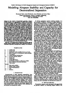
Figure 2: (a) two concurrent behaviors serialized in a single process with total latency m + n; (b) partitioned into two processes in a pipeline fashion with latency smaller than m + n (note that process 2 can start even before process 1 nishes). dress FIFOs, cell counter, and copy cell ag. To develop a behavioral model good for high-level synthesis, this complex design needs to be partitioned rst into subsystem, or modules, to reduce complexity such that each module can be modeled and synthesized e�ciently. This has been reported recently as well in a separate study by Vahid et al. [7] which shows the advantage of partitioning in terms of faster synthesis time and better overall design quality. Each module in the partition can be modeled as a process in VHDL. In VHDL, a process executes concurrently with other processes, but only sequential statements are allowed inside a process, which can undergo scheduling and allocation by high-level synthesis. Therefore, to model the entire partitioned system, multiple communicating processes are needed with frequent interactions among them. Two major criteria are exploited for partitioning the ATM switch system. The rst criterion is based on clocking (sw clk or HW clk) and functionality. One common limitation in current synthesis is that only one single clock signal can be used for each process. So, clocking, as well as functionality of each component as illustrated in Figure 1, are exploited to obtain an initial partition. The second criterion is based on pipeline throughput requirement of the two main channels. In the above initial partition, if modules WC and RC are each modeled by a single process, the concurrent behavior inside WC and RC has to be temporally serialized. Such serialization can impose longer delay than the maximal latency constrained by pipeline processing of the cell words in the switch core. This situation is illustrated in Figure 2. So, despite the lack of detailed circuit information for scheduling at this level of abstraction, a coarse partitioning of WC and RC into pipeline stages can be performed 3 ATM Switch Behavioral Modeling to derive a behavior model with higher pipeline concurDeveloping a behavior model with consideration of rency. target design features is essential to achieving success- 3.2 Multiple Clocking ful high-level synthesis. This section discusses the maDi�erent clocks for internal processing (by sw clk) jor issues associated with modeling the ATM switch for high-level synthesis. The behavior model of the entire and external transmission (by HW clk) draw a clocking ATM switch design is then developed, which consists of boundary in the design, as shown by the dotted square 26 communicating processes in about 1500-line VHDL in Figure 1. On either side of this boundary, processes are designated to model functionalities clocked by either codes. sw clk or HW clk. Therefore, when a cell being pro3.1 System Partitioning and Modeling cessed moves across the clocking boundary, a protocol The ATM switch is a complex design which consists for clock rate conversion to synchronize operation rates of a number of components operating concurrently for needs to be devised and modeled. Without such mechthe highways to access and update the cell FIFO, ad- anism, cell words could be missed or misaligned from
Figure 1: 2-channel ATM switch architecture. iHW0 or iHW1 rst takes serial-to-parallel (S/P) conversion to reduce to the slower processing rate sw clk. This received cell is then written into a cell FIFO for bu�ering, and will later be switched to an appropriate output highway based on the routing information contained in the header eld of the cell. When a cell is ready to be sent out, parallel-to-serial (P/S) conversion is performed at the output port to re-match the faster highway clock rate HW clk. When the received cell is written into the cell FIFO for bu�ering, its FIFO address is determined by Write Control WC and Write Address FIFO WAF. Namely, WC obtains from WAF the the next available address of the cell FIFO where a new cell can be written. Then, based on the destination of the cell, this address is kept in a Read Address FIFO RAF0 or RAF1, where the switch can later nd the address of the cell to be sent out. The address is kept in RAF0 if the cell is switched to oHW0, or in RAF1 if the cell is switched to oHW1, or in both if the cell is a copy cell switched for both output highways. To send a cell from the cell FIFO to the output highway oHW0 (or oHW1), Read Control RC is instructed by a read-out signal received from the extended highway exHW0 (or exHW1) to get the top cell address stored in RAF0 (or RAF1). The corresponding cell is then retrieved from the cell FIFO, and sent to oHW0 (or oHW1). After this cell is read out, the used address can be recycled to WAF, which is used later to store other cell received at iHW0 or iHW1. The switch core also has a cell counter wBC to monitor the available capacity of the cell FIFO. If the switch attempts to write a cell to the cell FIFO which is full, an alarm signal is sent to notify a central switch controller, which is not included in the switch design, to handle such exception. Furthermore, to keep track if a cell written into the cell FIFO is a copy cell, a 1-bit copy cell ag ccf is associated with each location in the cell FIFO.
16b
iHW0
reg0
reg1
reg2
48b
48b
48b
begin -- conversion at reg1 of iHW0 wait until (HW_clk'event and HW_clk='1'); reg1_ready