IEEE JOURNAL OF SOLID-STATE CIRCUITS, VOL. 49, NO. 9, SEPTEMBER 2014
2067
A 1000 fps Vision Chip Based on a Dynamically Recon¿gurable Hybrid Architecture Comprising a PE Array Processor and Self-Organizing Map Neural Network Cong Shi, Student Member, IEEE, Jie Yang, Ye Han, Zhongxiang Cao, Qi Qin, Liyuan Liu, Member, IEEE, Nan-Jian Wu, Member, IEEE, and Zhihua Wang, Senior Member, IEEE Abstract—This paper proposes a vision chip hybrid architecture with dynamically recon¿gurable processing element (PE) array processor and self-organizing map (SOM) neural network. It integrates a high speed CMOS image sensor, three von Neumann-type processors, and a non-von Neumann-type bio-inspired SOM neural network. The processors consist of a pixel-parallel PE array processor with parallelism, a row-parallel row-processor (RP) array processor with parallelism and a thread-parallel dual-core microprocessor unit (MPU) with parallelism. They execute low-, mid- and high-level image processing, respectively. The SOM network speeds up high-level processing in pattern recognition tasks by , which improves the chip performance remarkably. The SOM network can be dynamically recon¿gured from the PE array to largely save chip area. A prototype chip with a 256 256 image sensor, a recon¿gurable 64 64 PE array processor/16 16 SOM network, a 64 1 RP array processor and a dual-core 32-bit MPU was implemented in a 0.18 m CMOS image sensor process. The chip can perform image capture and various-level image processing at a high speed and in Àexible fashion. Various complicated applications including M-S functional solution, horizon estimation, hand gesture recognition, face recognition are demonstrated at high speed from several hundreds to 1000 fps. Index Terms—Dynamic recon¿guration, hybrid architecture, multiple levels of parallelism, pattern recognition, processing element (PE), SOM neural network, vision chip.
I. INTRODUCTION
T
HE vision chip [1]–[3] is a device integrating image sensor and parallel image processor on a single chip. It overcomes serial image transmission and serial image processing bottlenecks in traditional vision systems. It can achieve Manuscript received February 25, 2014; revised April 29, 2014; accepted June 01, 2014. Date of publication July 11, 2014; date of current version August 21, 2014. This paper was approved by Associate Editor Hideto Hidaka. This work was supported by the National Natural Science Foundation of China (Grant No. 61234003), and Special Funds for Major State Basic Research Project of China (No. 2011CB932902). C. Shi, J. Yang, Y. Han, Z. Cao, Q. Qin, L. Liu, and N.-J. Wu are with the State Key Laboratory for Superlattices and Microstructures, Institute of Semiconductors, Chinese Academy of Sciences, Beijing 100083, China (e-mail:
[email protected]). C. Shi is with the Department of Electronic Engineering, Tsinghua University, Beijing 100084, China. Z. Wang is with the Department of Electronic Engineering and the Institute of Microelectronics, Tsinghua University, Beijing 100084, China. Color versions of one or more of the ¿gures in this paper are available online at http://ieeexplore.ieee.org. Digital Object Identi¿er 10.1109/JSSC.2014.2332134
an image processing rate higher than 1000 frames per second (fps) and can be widely applied in industry automation, security monitoring, robotic vision, etc. The vision chips can be classi¿ed into application-speci¿c and programmable ones. The application-speci¿c vision chip is dedicated for one application (e.g., motion tracking [4], depth imaging [5], image compression [6], contrast extraction [7], [8], eye tracking [9], horizon estimation [10] and moving detection [11]), while the programmable vision chip can handle multiple applications through software programming [12]–[21]. According to the processing circuit type, the vision chips can be classi¿ed into analog and digital ones. The analog vision chips achieve compact chip area and lower power consumption [7]–[10], [12], [14]–[17]. While the digital chips show higher performance in terms of precision, Àexibility and robustness [4]–[6], [11], [13], [18]–[21]. In fact, with the technology progress, the chip area and power consumption for digital processing circuits has shrunk remarkably. Therefore this paper focuses on the programmable vision chip with digital processors. Most programmable vision chips adopted the architecture of a two-dimensional (2D) processing element (PE) array [3], [12], [14]–[17]. Each PE consists of a photodiode and a processing circuit. The PE array operates in a single-instruction multipledata (SIMD) fashion. It performs image capture and pixel-parallel low-level image processing (e.g., image ¿ltering and mathematic morphology). Some vision chips integrated dedicated circuits in addition to the SIMD PE array to perform mid-level image processing (e.g., moment calculation [13], object location [18], feature statistics [19], and global transformation [20]). Recently, a programmable vision chip with multiple-level parallel processors was demonstrated [21]. This chip consists of a pixel-parallel PE array processor, a row-parallel row processor (RP) array processor and a non-parallel microprocessor unit (MPU). The three types of processors perform low-, mid- and high-level image processing, respectively. The PE and RP array processors can perform low- and mid-level processing at a high speed of less than 1 ms. But the high-level processing speed is limited by the serial MPU. The high-level image processing time is much longer than the low- and mid-level image processing time and much larger than 1 ms. Thus, according to the famous Amdahl’s Law [22], the system performance would be bottlenecked by the high-level processing.
0018-9200 © 2014 IEEE. Personal use is permitted, but republication/redistribution requires IEEE permission. See http://www.ieee.org/publications_standards/publications/rights/index.html for more information.
2068
IEEE JOURNAL OF SOLID-STATE CIRCUITS, VOL. 49, NO. 9, SEPTEMBER 2014
Many high-level algorithms involve complicated bottleneckinducing image feature recognition tasks. And various arti¿cial neural networks are effective tools to solve these tasks quickly and robustly [23]–[25]. Unlike a serial MPU based on the vonNeumann architecture, a neural network is a simpli¿ed model of the human brain, and is expert in the pattern recognition. These bio-inspired neural networks should ¿rst be trained on known feature patterns, and then can quickly give recognition results of other unknown patterns, with enough tolerance to random pattern variations. Moreover, these neural networks have intrinsic massive vector-parallelism for hardware implementation, and outperform the serial MPU to a large extent on the feature recognition speed. Therefore the hardware neural networks have the potential to overcome the performance bottleneck in most highlevel image processing. So far, some vision chips have already employed the cellular neural networks for image processing [12]. However, as to our knowledge, such neural network is only suitable for image enhancement and image segmentation in the low- and mid-level processing on the vision chips, and makes no contribution to the high-level processing acceleration. This paper proposes a high speed programmable vision chip based on a dynamically recon¿gurable hybrid architecture comprising a PE array processor and self-organizing map (SOM) neural network [26]. The vision chip integrates two types of processors: 1) von Neumann-type processors: a pixel-parallel PE array processor, a row-parallel RP array processor, and a threadparallel dual-core MPU; and 2) non-von Neumann-type processor: an SOM neural network. The PE array and RP array processors can carry out the low- and mid-level image processing, respectively. The SOM neural network together with the dualcore MPU could perform the high-level image processing and improve the processing speed remarkably. The SOM neural network can be trained online through the learning vector quantization (LVQ) method. Because the PE array processor and the SOM neural network operate in time-division multiplexing, they can be recon¿gured dynamically from each other so that the area of the vision chip can be reduced effectively. The SoC vision chip can perform image capture, and low- to high-level image processing at a high speed and in Àexible fashion. The vision chip can achieve a processing speed of over 1000 fps. This chip can be applied in complicated vision applications including hand gesture recognition and human face detection. This paper proceeds as follows. In Section II, the system architecture of the proposed vision chip is described. Section III presents the circuit designs of some important modules. The experimental results of the prototype chip with complicated vision applications are demonstrated in Section IV. The chip performance and work comparison are discussed in Section V. Finally, Section VI concludes this paper.
pixel array and a The image sensor contains an column of analog-to-digital converters (ADCs). The von Neumann-type processors consist of an pixel-parallel PE array processor, an row-parallel RP array processor, and a thread-parallel dual-core MPU. They perform the low-, midand high-level image processing, respectively. The non-von Neumann-type SOM neural network with neurons is a simpli¿ed model of the human brain. It performs the vector-parallel image recognition tasks and remarkably speeds up the high-level image processing. The digital image data is ¿rst captured by the image sensor. The image data in a pre-de¿ned Region-of-Interest (ROI) is selectively loaded into the PE array processor. The selection of ROI is implemented by the Àexible pixel-PE mapping relationship, as will be detailed in Section II.B. The 2D SIMD PE array processor performs pixel-parallel low-level image processing and increases the processing speed by . Each PE consists of a 1-bit ALU and a small size local memory. It is connected to its four nearest-neighbor PEs on east, south, west and north. The RP array processor performs row-parallel mid-level processing to extract image features by speedup of . Each RP is an 8-bit ALU-based processor and can access its nearest upper and lower RPs, as well as the rightmost PE in the same row. Moreover, some non-adjacent RPs can directly access each other to accelerate global operations by a skip chain, as will be shown in Section III.C. The dual-core MPU is used to perform high-level image processing and to manage overall chip operation. The two cores can visit their private memories simultaneously in thread-parallel, and visit the global data bus alternately in an arbitration way. Its processing result is outputted through the I/O memory and used to dynamically adjust the sensor parameters on chip [21]. However, the MPU is dif¿cult to ¿nish high-level complicated pattern recognition tasks on time to match with the processing speed of the PE and RP array processors. So an SOM neural network with neurons is proposed to speed up the high-level recognition task by in vector-parallel. The SOM neuron plane is partitioned into several non-overlapping regions, and each of these regions corresponds to a feature class. In the SOM neural network, each neuron stores a -dimension reference vector (RV): , where represent the neuron coordinate. The SOM neural network can be trained online by the LVQ method [27]. For each training iteration, one feature vector (FV): with its already-known pattern class is broadcasted to the neural network. Then all neurons simultaneously compute the vector distances as
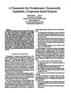
II. CHIP ARCHITECTURE (1) A. System Architecture Fig. 1 shows the hybrid architecture of the proposed vision chip. It consists of a high-speed image sensor, three von Neumann-type multiple-level parallel processors and a bio-inspired non-von Neumann-type SOM neural network.
The neuron with the minimum distance is regarded as the winner and the region of its location represents the recognized pattern class of the FV. The ¿nal class information is obtained in the MPU by looking up a location-class index table pre-stored in
SHI et al.: A 1000 fps VISION CHIP BASED ON A DYNAMICALLY RECONFIGURABLE HYBRID ARCHITECTURE
2069
Fig. 1. Proposed vision chip architecture.
the MPU memory. If the recognized class is consistent (inconsistent) with its already-known class, the RVs of those neurons within the winner neighborhood are simultaneously updated towards (against) the FV:
(2) The neighborhood size and the learning rate are gradually decreased along the training iterations for convergence. Once trained, the SOM neural network can recognize other FVs extracted from real-time sensor images by identifying the winner neuron with (1). The hardware implementation of the SOM neural network usually consumes considerable chip area [24]. However, because the PE array processor and the neural network operate in time-division multiplexing, we propose a shared recon¿gurable circuit to dynamically recon¿gure the von Neumann-type PE array processor and the non-von Neumann-type neural network from each other. Thus the vision chip can enhance computational capability and speeds up the image processing ef¿ciently at the cost of few additional logic gates and clock cycles. Each sub-array of 4 4 PEs can be recon¿gured as an SOM neuron. So the SOM neural network has neurons. The details will be discussed in Sections II.B and III.A. B. Architecture Features 1) Hybrid Architecture: The proposed vision chip integrates both von Neumann-type processors and non-von Neumann-type SOM neural network processor. Among the von Neumann-type processors, it is dif¿cult for the dual-core MPU to ¿nish the high-level complicated pattern recognition tasks
on time to match with the processing speed of the PE and RP array processors, due to the famous von Neumann bottleneck. It results from executing the instructions in sequence and the shared bus between the program memory and data memory. In contrast, the SOM neural network can speedily and ef¿ciently carry out the pattern recognition tasks. The SOM network is a competitive neural network and mimics human brain’s visual system function that abstracts and recognizes input patterns by spatially partitioned neuron-map quickly and robustly [27]. All of its neurons can operate simultaneously in vector-parallel to speed up pattern recognition tasks by . The SOM neural network and the MPU can cooperate to ¿nish the high-level image processing on time to match with the processing speed of PE and RP array processors. Therefore, the vision chip based on the hybrid architecture can eliminate the high-level processing bottleneck in many vision applications and largely improve the system performance. 2) Recon¿gurable PE Array and SOM Neural Network Processor: The SOM neural network processor can be dynamically recon¿gured from the PE array processor. The PE array is partitioned into sub-arrays (see Fig. 2). Each sub-array contains 4 4 PEs and a conditional generator (CG). The solid and dashed paths are exclusively valid for the PE array and the SOM network, respectively. The signal controls the dynamic recon¿guration between the two processors by switching the paths among the PEs and the CG in only 3 clock cycles. In the PE array mode, the 16 1-bit grained PEs in one sub-array are connected in a 2D mesh, so that all of the sub-arrays constitute the PE array processor. In the SOM network mode, the 16 PEs in one sub-array is chained in a snake style, so that the sub-array is recon¿gured into one 16-bit grained SOM neuron. The bit-position (bp) of each PE
2070
IEEE JOURNAL OF SOLID-STATE CIRCUITS, VOL. 49, NO. 9, SEPTEMBER 2014
Fig. 3. The dependences of the areas of the tightly-coupled PE array pixel plus PE array on image sensor resolution and the separated parameter . Fig. 2. The topological structure of one PE sub-array with the dynamic recon¿guration capability for modes of PE array processor and SOM neural network.
in the neuron is marked in Fig. 2. The neuron can communicate with its neighboring neurons through their MSB and LSB PEs. Such inter-neuron communication is used to load RVs and output processing results. In this mode, all the sub-arrays constitute the SOM neural network. Section III.B will show the operation details of the neural network. The dynamic recon¿guration between the PE array and the SOM neural network largely saves the chip area. 3) Enhanced Multiple-Level Parallelism: Different image processing levels require processors with different types of parallelism. In the previous work [21], the low- and mid-level processing is effectively mapped onto pixel-parallel PE array with a speedup of , and a row-parallel RP array with a speedup of , respectively. But the high-level processing is left to a serial MPU with a serious von Neumann bottleneck for complicated pattern recognition tasks. Our chip enhances the parallelism by integrating an SOM neural network and a dual-core MPU. The high-level processing tasks can usually be decomposed into common pattern recognition and a few other speci¿c tasks. The pattern recognition tasks can be vector-parallelized by the SOM neural network with a remarkable speedup of . The speci¿c tasks can be thread-parallelized by the dual-core MPU with a speedup of . The combination of the SOM network and the dual-core MPU can effectively accelerate high-level processing. 4) Separated Image Sensor and Processor Architecture: Many vision chips adopted a pixel-PE tightly-coupled architecture that each PE element integrates one pixel along with one processing circuit unit [4]–[10], [12]–[18], [20]. Since the area of the processing circuit is much larger than that of the pixel, such architecture suffers from low sensor resolution and small ¿ll factor % . Our chip separates the pixel array from the PE array to beat the sufferings [28]. In the separated architecture, the sizes of the pixel array and PE array can be designed independently. Fig. 3 compares the area consumption
of the tightly-coupled architecture with PE array and the separated architecture with an pixel array plus an PE array. The parameters for the area estimation are listed in Fig. 3. The area of the tightly-coupled architecture increases drastically with so that the chip size is not acceptable when . However, the separated architecture can support higher sensor resolution till with a reasonable 0.18 m CMOS chip area. The separated architecture also increases the pixel ¿ll factor to 60% and improves the sensor image quality. Because the separated pixel array is usually larger than the PE array in array size, the PE array can process only one slice of the image at a time and has to ¿nish the whole image processing by scanning all the slices. This increases the low-level processing time. However, the low-level processing occupies only a small percentage of the overall processing time on the vision chip. Thus the system performance would not be much deteriorated, according to Amdahl’s Law [22]. Moreover, on the proposed vision chip, the image on the pixel array can be sub-sampled before they are transferred into the PE array. Fig. 4 shows the three Àexible mapping relationships between the pixel array and the PE array when , with different sample intervals and slice sizes. The sub-sampling manner can be dynamically changed by the MPU to emulate a bio-inspired glance-stare vision [28]–[30]: In the ¿rst frame, a 4:1 sub-sampled image in a large slice is roughly processed (glanced) to quickly locate the concerned object; Then in successive frames, only a 2:1 or 1:1 sub-sampled image in a smaller slice containing that object is further processed in detail (stared). III. DESIGN OF CIRCUITS A. PE Circuit Fig. 5 shows the recon¿gurable PE circuit. The PE circuit contains: 1) a 1-bit ALU; 2) two multiplexers op1_Mux and op2_Mux for ALU operands selection; 3) a carry register ; 4) a 1-bit temporary register ; 5) a 1-bit wide PE Memory; and 6) eight recon¿guration multiplexers (shaded in Fig. 5). The ALU
SHI et al.: A 1000 fps VISION CHIP BASED ON A DYNAMICALLY RECONFIGURABLE HYBRID ARCHITECTURE
Fig. 4. The Àexible mapping relationship between the
pixel array and the
Fig. 5. The PE circuit schematic. The Italic signals are from the PE instruction.
can perform the operations of full adder, inverter, AND gate and OR gate. The recon¿guration multiplexers can switch the topological connections between neighboring PEs for different recon¿guration modes. In the PE array processor mode, the signal op1_sel selects the ¿rst ALU operand from its own PE Memory, or from the PE Memorys in its east, south, west and north neighboring PEs. The register stores the ALU carry-out in current cycle and acts as the ALU carry-in for next cycle. Although only a simple 1-bit ALU is used, the PE can still realize multiple-bit operations by bit-serial processing [21]. B. SOM Neuron Circuit When the
PE array processor is recon¿gured as the SOM neural network, each sub-array with 4 4 PEs and a condition generator form one SOM neuron, as shown in Fig. 2. The condition generator consists of two Àag registers,
2071
PE array.
Fig. 6. The circuit schematic of the condition generator. The italic signals are from the array controller.
three AND gates and three multiplexers, as shown in Fig. 6. The Àag register in each neuron can be independently set by the array controller. The condition generator produces necessary signal bits for the conditional operations of the SOM neuron. In the SOM neuron, the 16 1-bit ALUs of the 16 PEs constitute an equivalent 16-bit ALU. In the 16-bit ALU, the 1-bit ALU carry-out of the PE at the th bit-position is directly used as the 1-bit ALU carry-in of the PE at the th bit-position in one clock cycle, so that a 16-bit ripple-adder is achieved. The PE Memorys and registers in the 16 PEs also constitute a 16-bit wide memory and a 16-bit T register, respectively. For each PE in the SOM neuron, the ¿rst ALU operand comes from its own PE Memory, from the PE Memorys of its two bit-neighboring PEs, or from the corresponding bit-slice of the FV bus. Table I lists the LL, LH, AH input connections of PEs at different bit-positions of the neuron. These connections enable data shift
2072
IEEE JOURNAL OF SOLID-STATE CIRCUITS, VOL. 49, NO. 9, SEPTEMBER 2014
TABLE I THE CONNECTIONS BETWEEN NEIGHBORING PE IN THE SOM MODE
Fig. 8. The circuit schematic of the row processor.
Fig. 7. Critical calculations for the SOM neurons with . (a) Computing valid bits) of the absolute-difference (AD) between the th-components ( feature vector (FV) and the reference vector (RV). (b) Clamping updated refer. ence vector component RV(p) to
for multiplication/division and neuron I/O. The second ALU operand is selected among and signals. The SOM neural network can be trained online by the LVQ method as follows (The vector components must be in unsigned ¿xed-point format): (1) Loading initial reference vectors The initial RVs are randomly generated and shifted into the neural network via the inter-neuron communications; (2) Broadcasting feature vector and computing vector distance First the Àag registers in all neurons are set to 1. And then a training FV with already-known class is broadcasted to all neurons through the FV bus in a component-serial fashion. Each neuron simultaneously computes the absolute-difference (AD) between the th-components of the FV and its RV, as illustrated in Fig. 7(a), and accumulates the AD value to the vector distance variable Dist. After the index runs from 0 to in (1), the ¿nal Dist is obtained; (3) Determining winner neuron: The winner neuron with the minimum Dist is determined by the RP array processor in row-parallel; (4) Updating reference vectors First the neurons outside the winner neighborhood are disabled by setting their
Fig. 9. Mid-level acceleration with proposed techniques of PE-condition and skip chain in RP array. (a) The benchmark algorithm of binary image area calculation performed by the PE and RP arrays. (b) The performance improvement with proposed techniques.
Àag registers to 0. Then the RVs of the neurons within the winner neighborhood can be updated by (2) in a component-serial fashion. The multiplication by can be approximated by adding up proper shifted versions of the multiplicand without multipliers.
SHI et al.: A 1000 fps VISION CHIP BASED ON A DYNAMICALLY RECONFIGURABLE HYBRID ARCHITECTURE
2073
Fig. 10. Schematic of 4-T pixel and the block diagram of the 10-bit cyclic ADC in one row of the image sensor.
Fig. 12. The measurement system.
C. Row Processor
Fig. 11. The microphotograph of the prototype vision chip.
The steps (2)–(4) should be repeated until some prede¿ned convergence criterions are satis¿ed. After the network is trained and the Àag registers in all neurons are set to 1, the SOM neural network can be used to recognize the FV of the real-time sensor images by the above (2) and (3) steps. We have to optimize a tradeoff between the vector dimension and the number of valid bits per component in the neural network under limited hardware resources. If the RV or FV is a 16D vector, the valid bits per vector component must be limited to no more than 12 to avoid overÀow when evaluating (1). So each updated component must be clamped back to the range of in every training loop, as shown in Fig. 7(b). The clamping operation with other numbers of valid bits is also possible with proper bit-shifting.
The RP circuit consists of an 8-bit ALU, an 8-bit buffer, an 8-bit wide RP memory constructed by a bank of registers, three multiplexers and some condition Àag registers, as shown in Fig. 8. Each RP can access its nearest upper and lower RPs through the ¿rst ALU operand selection. Moreover, every 4th RP in the RP array has extra access to its 4th neighboring upper and lower RPs. Thus an RP skip chain is formed for global operation acceleration, as mentioned in Section II. The buffer is used as the interface between the RP and PEs on the same row, as well as the interface between the RP array processor and the MPU. The Àag enables the PE-condition operation by establishing a more ef¿cient data path between the PE and RP to accelerate feature extraction. The ALU can perform addition, subtraction, as well as max/min extraction for non-linear operations like medium ¿ltering, grayscale morphology and SOM winner neuron determination. Fig. 9(a) shows how the PE-condition operation along with the RP skip chain signi¿cantly accelerates the mid-level feature extraction. The binary image area calculation is used as the benchmark algorithm. First, each RP counts the pixels with
2074
IEEE JOURNAL OF SOLID-STATE CIRCUITS, VOL. 49, NO. 9, SEPTEMBER 2014
TABLE II CHIP CHARACTERISTICS
Fig. 13. A 256 80 MHz.
logic 1 in each PE row by the PE-condition operation in rowparallel. Then the counts in each RP group are summed up and stored into the corresponding skip RP. Finally, the skip RPs gather all the summations into the ¿nal area. Fig. 9(b) shows the performance improvement by using the acceleration techniques on a 64 64 PE array and a 64 1 RP array with a skip interval of 4. Without the PE-condition operation, each 1-bit binary data in the PE array must be patched with seven extra bits of 0 to form an 8-bit data transferred via the RP buffer, which is very time-consuming. Fig. 9(b) indicates that the PE-condition technique reduces 53% of clock cycles from 820 down to 380, and the skip chain technique further reduces 50% of cycles from 380 down to 190. Thus a total % acceleration is achieved. D. High-Speed Image Sensor The high-speed image sensor consists of a pixel array and row-parallel readout circuits. Fig. 10 shows the schematic of the pixels and the readout circuit in one row. The pixel is a 4-T CMOS active pixel [31]. The readout circuit consists of a correlated double sampling (CDS) block, a programmable gain ampli¿er (PGA) block and an analog-to-digital convertor (ADC). When pix_rst and sel signals are high, and Tx signal is low, the
256 raw image captured by the vision chip under 2000 fps at
reset voltage can be sampled by the readout circuit. Alternatively, when Tx and sel are high, and pix_rst signal is low, the photo-sensed voltage from the photodiode (PD) can be sampled. Thus the CDS function is achieved and the ¿xed pixel noise is reduced. The ADC is a small-area cyclic ADC with a PGA ampli¿er. The reason for choosing the cyclic ADC structure is that it can achieve higher speed than the ramp-sweep ADCs to realize 1000 fps image readout, and it consumes less area resource than the SAR ADCs. In fact, many reported high-speed image sensors have adopted the cyclic ADC structure [32]–[35]. The PGA ampli¿er can reduce required pixel integration time to increase the sensor frame rate, and extend dynamic range for better image quality. The ampli¿er gain can be programmed by the MPU. The CDS and PGA blocks can share some circuit resource with the ADC kernel. Therefore the total area of the readout circuit can be effectively reduced. IV. IMPLEMENTATION AND MEASUREMENT RESULTS A. Chip Implementation and Measurement System A prototype vision chip was implemented in a 1P5M 0.18 m CMOS image sensor technology, as shown in Fig. 11. This chip contains a 256 256 pixel array, two 128 10-bit ADC arrays with CDS and PGA circuits, a recon¿gurable 64 64 PE array and 16 16 SOM neural network processor, a 64 RP array processor with a skip interval of 4, a dual-core 32-bit RISC MPU, and many testing circuits distributed over the chip. The large pixel photodiodes shortens the integration time below 1 ms. The image lag is suppressed by dedicated pixel layout design and technology process optimization [31]. The measurement system for the vision chip is shown in Fig. 12. The prototype chip is packaged on PCB boards and linked to an FPGA chip for communication with a monitor PC. We have developed software tools for compiling and downloading vision chip instructions. lux lightening strength was projected onto the target objects and their surroundings throughout the following chip measurement. The chip characteristics are summarized in Table II.
SHI et al.: A 1000 fps VISION CHIP BASED ON A DYNAMICALLY RECONFIGURABLE HYBRID ARCHITECTURE
Fig. 14. Some experimental results of basic low- and mid-level image processing.
Fig. 15. Complex ¿ltering.
The typical working frequency is 50 MHz. The power consumption is about 630 mW when running 1000 fps image capture and processing. The pixel dynamic range is mainly limited by the 8-bit ENOB of the ADC. The PE and RP array processors contribute 12 and 1.6 giga operations per second (GOPS) to lowand mid-level processing for 8-bit arithmetic operations, respectively. The SOM neural network contributes as much as 45.4 and 31.6 kilo recognitions per second (KRPS) for 16D and 32D FVs, respectively. Such high-level processing speed can satisfy most vision applications under 1000 fps restriction. B. High Speed Image Capture and Basic Low-, Mid-Level Image Processing Fig. 13 shows a 256 256 raw image captured by the highspeed image sensor on the chip at 2000 fps. The image sensor can work alone under an 80 MHz clock, which is higher than the
Fig. 16. Salient edge extraction based on M-S functional.
2075
2076
IEEE JOURNAL OF SOLID-STATE CIRCUITS, VOL. 49, NO. 9, SEPTEMBER 2014
50 MHz chip system clock. The image data is directly outputted via dedicated testing ports without any on-chip processing. The high quality of raw image ensures the robustness and precision of subsequent image processing. The vision chip can implement common basic low- and mid-level image processing algorithms such as spatial ¿ltering, thresholding and morphology, as shown in Fig. 14. C. Complex Filtering From this subsection on, we focus on the chip’s real-time ability to perform more complicated algorithms. The ¿rst one is the complex ¿ltering [36] by solving the image from: (3) where represents the iteration number, and denotes real part. The ¿ltering is performed by the PE array processor in pixel-parallel. Fig. 15 shows the results. 64 64 image captured by the image sensor with the 4:1 sample manner is used. The real part is gradually blurred while the imaginary part exhibits gradually distinct edges. Each iteration consumes 2.7 s at 50 MHz. Fig. 17. Horizon estimation.
D. Salient Edge Extraction Based on M-S Functional The Mumford-Shah (M-S) functional is a very complicated mid-level algorithm [37]. To make the functional more compatible with the parallel vision chip architecture, we have modi¿ed it as:
(4) where are the input image, the smoothed image and the salient edge binary image, respectively, and are user-de¿ned weights, denotes the whole image. The goal is to seek the optimized and images that lead to the minimum . We solve the functional on our vision chip as follows. At every iteration , the image is generated by performing a Gaussian ¿lter on in the previous iteration. Note , which is a 64 64 image captured by the image sensor with the 4:1 sample manner. The gradient in (4) is realized by Sobel ¿ltering. The is generated by thresholding . After the PE array processor generates and images, the RP array processor sums up the pixels in the three images. The MPU computes and stops iterations when minimum is achieved. Fig. 15 shows the processing result. Each iteration consumes 46 s at 50 MHz. The solution can be ¿nished in 1 ms as iterations are seldom met. E. Horizon Estimation The visual horizon estimation has already been implemented by an application-speci¿c vision chip with low pixel resolution (12 12) and low frame rate (25 fps) [10]. We modify the algorithm in [10] to make it more computationally ef¿cient on our chip. For every frame, the pixel in each location is ¿rst clustered as either a sky or ground pixel according to the horizon
(originated at the middle point equation in the last row of the image, with east and north directions as x- and y-axis) estimated in the previous frame. Then the average pixel values of the two clusters are computed. Next, the pseudo-ground pixels in the left half image plane are counted as psGndLeft. A pseudo-ground pixel is a ground-cluster pixel with its value closer to the sky average than the ground average. psGndRight, psSkyRight and psSkyRight are similarly counted. Finally, the horizon parameters are updated by:
(5a) (5b) where and are updating rates. The cluster generation, cluster average computation and pseudo pixel counting are performed by PE and RP array processors. The parameter updating is simply performed by the MPU. By this algorithm, the estimated horizon can quickly approach to the real horizon within one to several frames. Fig. 16 shows the estimation results. The Àight scenes are simulated by playing Àight videos in front of the sensor. Although the algorithm is performed on 64 64 images with 4:1 sample manner, the PC draws red-bold horizon lines on the original 256 256 images for visual clarity. The image capture and processing consumes 0.65 and 0.24 ms, respectively. Thus fps horizon estimation can be achieved. F. Hand Gesture Recognition and Tip Tracking A hand gesture recognition algorithm was implemented to demonstrate the real-time recognition capability of the SOM neural network. Seven types of hand gestures are used, de¿ned as Grasp, Yeah, Up, Fist, Palm, Index and Down, respectively
SHI et al.: A 1000 fps VISION CHIP BASED ON A DYNAMICALLY RECONFIGURABLE HYBRID ARCHITECTURE
2077
Fig. 18. 1000 fps hand gesture recognition on the vision chip. (a) Algorithm Àow. (b) Some recognition results. (c) Lecture Powerpoint control. (d) Remote video games. (e) Non-contact writing and drawing.
[38]. The algorithm is brieÀy illustrated in Fig. 18(a). First, a sub-sampled 64 64 hand image is captured by the image
sensor. Then, a binary hand gesture is obtained by some preprocessing. Next, a 64D Projected Principle-Edge Distribution
2078
IEEE JOURNAL OF SOLID-STATE CIRCUITS, VOL. 49, NO. 9, SEPTEMBER 2014
Fig. 19. Some results of human face detection and recognition. (a) Some results of Face detection. (b) Some face samples from the training library for face recognition. (c) Some results of face recognition.
(PPED) feature vector [39] is extracted from this binary image. The 64D feature vector is then compressed into a 16D format by averaging every four successive components. Finally, the PPED vector is sent to the SOM neural network for recognition. If an Index gesture is recognized, a tip tracking algorithm is appended to locate the uppermost point of the ¿ngers. The consumed time shown in Fig. 18(a) promises a high frame rate of fps. Such high frame rate facilitates robustness improvement by frame-level low-pass semantic ¿ltering, which is unfeasible in low-frame-rate vision systems. We had invited 6 people to contribute more than 100 binary training images for each class of the hand gesture to train the SOM neural network online. And the vision chip with the trained SOM neural network were used to recognize 1200 hand gesture images captured from 12 people in the real world. The ¿nal recognition accuracy is %. Fig. 18(b) shows some recognition results and Fig. 18(c)–(e) shows some interesting human-machine interactions based on the hand gesture recognition. G. Human Face Detection and Recognition The vision chip can realize human face detection for the subway pedestrian statistics system. As the pedestrians all step downward on the entrance staircase, so we can restrict the detection region to the middle 256 64 pixel stripe with properly setting the lens, as indicated in Fig. 19(a). The detection stripe is partitioned into 7 half-overlapping 64 64 windows,
and one window is sampled and processed in one frame. One human face can be detected if its majority part falls within any of these windows. The face detection is essentially a 2-class problem: face class and non-face class. A 32D PPED feature vector is directly extracted from a grayscale window image, and then sent to the SOM neural network for recognition. Fig. 19(a) shows some face detection results in our lab. In this algorithm, we used the standard ORL human face library [40] to train the SOM neural network in an off-line way. The detection accuracy is about 86%. This is obtained by counting the successfully detected human faces versus all the faces that have appeared in the middle 256 64 image stripe during the detection. The faces passing through this stripe were required to be within head rotation and % size variance from the 64 64 resolution. The image capture and processing time for one window is 0.6 ms and 0.25 ms, respectively. So it totally consumes ms to process the whole 256 64 stripe in 7 frames. The vision chip can also realize face recognition among a small group of persons based on similar algorithm. The face recognition can be used in identi¿cation systems, which would require the human faces appear in a dedicated location such as the central 128 128 pixel region. So we can use 64 64 images captured by the image sensor with 2:1 sample manner on the central 128 128 region. We used 100 face images for each person to train the SOM neural network online. These face images were
SHI et al.: A 1000 fps VISION CHIP BASED ON A DYNAMICALLY RECONFIGURABLE HYBRID ARCHITECTURE
2079
TABLE III COMPARISON WITH THE STATE-OF-THE-ART VISION CHIPS
), different captured under different head rotations (within % face sizes) and different expressions. distances (within Fig. 19(b) shows some face samples from the target person group for training, and Fig. 19(c) shows some recognition results. The human faces to be recognized were required to be within head rotation and % size variance to match with the training images. It takes 0.85 ms per frame and the recognition accuracy is also about 86%. The accuracy ¿gure is obtained in a similar way as that in the face detection. V. PERFORMANCE AND COMPARISON The vision chip based on the dynamically recon¿gurable hybrid architecture can execute image capture to low-, mid- and high-level image processing at a high speed of over 1000 fps and in Àexible fashion. The SOM neural network removes the high-level image processing bottleneck in complicated pattern recognition tasks and improves the system performance of the chip remarkably. Moreover, the SOM neural network can be dynamically recon¿gured from the PE array processor. This realizes the recon¿guration between the non-von Neumann and von Neumann-type processors, and saves the chip area effectively. The experimental results of various complicated algorithms demonstrated that the vision chip has high system performance from high speed image capture to fast high-level image processing.
In hand gesture and face recognitions, the SOM network has reduced the high-level recognition time by as much as 98% when compared with the dual-core MPU (Fig. 20(a)). If only the MPU is used, the recognitions cannot achieve 1000 fps. Moreover, with the increase of feature vector dimension, the recognition time on the MPU increases drastically (Fig. 20(b)–(c)), and would cause a serious high-level processing bottleneck in system performance. In contrast, the recognition time on the SOM network only exhibits a mild increase, which still matches well with the low- and middle-level processing time on PE and RP arrays, and would not degrade the system performance. The recon¿guration capability af¿liated to the PE array processor remarkably reduces the additional area cost for integrating the 16 16 SOM neural network from mm [24] to only 1.6 mm under typical 0.18 m process. The recon¿guration technique can also be applied in those pixel-PE tightly-coupled vision chips to obtain high-level processing capabilities with very small area overhead. However, compared with a standalone SOM neural network, the recon¿gured SOM neural network lacks the capability of nonlinear operation for determining the winner neuron. The RP array processor performs the required nonlinear operations. This would consume a little more time than in [24]. Table III compares the proposed vision chip with other state-of-the-art digital programmable vision chips. Our chip
2080
IEEE JOURNAL OF SOLID-STATE CIRCUITS, VOL. 49, NO. 9, SEPTEMBER 2014
SOM neural network makes our chip reach the highest system performance reÀected by a FOM value. The FOM value considers the weights of low, middle and high-level processing speed in a reasonable way for evaluating the system performance. On the previously reported vision chips [18]–[21], the speed of the high-level recognition tasks (reÀected by the KRPS ¿gure) could not match the speed from low- to mid-level processing (reÀected by the GOPS ¿gure). Our proposed chip aims to solve such mismatch problem, and ¿nally achieves high system performance from image capture up to high-level image processing. Although the GOPS ¿gure for the low- and mid-level processing speed on our chip is not the highest among all the vision chips, it is suf¿cient to reach 1000 fps system-level performance, as indicated in Table III. The other vision chips, however, either lack of on-chip high-level processing ability [18], [20], or fail to achieve 1000 frames per second when complex recognition tasks are required [19], [21]. The prototype chip area of 82.3 mm is larger than the other chips. However, if we remove the additional testing circuits in the next version, the chip area can be reduced ef¿ciently. The power consumption of the proposed vision chip is higher than the others because of its largest pixel array size, highest ADC resolution and largest PE array size among all the chips. Moreover, the processing circuit in the proposed chip is not designed by full custom currently and many testing circuits are distributed all over the chip. This also contributes to higher power consumption. We will focus on the low-power optimization in our next vision chip design. VI. CONCLUSION
Fig. 20. The performance comparison between the SOM neural network and the dual-core MPU in the high-level recognition tasks. (a) The consumed recognition time in hand gesture hand face recognition. (b) The consumed time for different dimensional feature vectors. (c) The KRPS index for different dimensional feature vectors.
has the highest image resolution, highest pixel ¿ll factor, most levels of parallelism, and novel dynamic recon¿guration. The
A high speed vision chip based on a dynamically recon¿gurable hybrid architecture comprising the PE array processor and SOM neural network was proposed. The SoC vision chip integrates a high speed image sensor, three von Neumann-type processors, and a non-von Neumann-type SOM neural network. The three von Neumann-type processors are a PE array processor with an parallelism, a RP parallelism and a dual-core array processor with an MPU with an parallelism, respectively. The SOM neural network speeds up the high-level image processing in comand implicated pattern recognition tasks by proves the system performance of the vision chip. The chip can perform image capture and low-, mid-, high-level image processing at a high speed of fps. Moreover, the SOM neural network and the PE array processor can be dynamically recon¿gured from each other to effectively save chip area. The prototype chip with a 256 256 image sensor, a recon¿gurable 64 64 PE array and 16 16 SOM neural network processor, a 64 1 RP array processor and a dual-core 32-bit RISC MPU has been implemented in a 0.18 m CMOS image sensor technology. The power consumption was 630 mW at 50 MHz. The SOM neural network delivered KRPS for complicated recognition tasks in the high-level processing. The vision chip implemented various complicated applications including M-S functional solution, horizon estimation, hand gesture recognition, face detection and recognition at a high speed from
SHI et al.: A 1000 fps VISION CHIP BASED ON A DYNAMICALLY RECONFIGURABLE HYBRID ARCHITECTURE
several hundreds to fps. The results demonstrated that the vision chip can achieve high system performance from image capture to high-level image processing. Therefore, the proposed vision chip is a promising candidate to prevalently replace the traditional vision systems. For example, the vision chip can replace the traditional vision systems in industrial automation to improve inspection speed, as well as in high-speed target tracking. REFERENCES [1] C. Mead, “Neuromorphic electronic systems,” Proc. IEEE, vol. 78, no. 10, pp. 1629–1636, 1990. [2] K. Aizawa, “Computational sensors—Vision VLSI,” IEICE Trans. Inf. Syst., vol. E82D, no. 3, pp. 580–588, 1999. [3] M. Ishikawa, K. Ogawa, and T. Komuro, “A CMOS vision chip with SIMD processing element array for 1 ms image processing,” in 1999 IEEE Int. Solid-State Circuits Conf. (ISSCC) Dig. Tech. Papers, San Francisco, CA, USA, 1999, pp. 206–-207. [4] T. Komuro, I. Ishii, M. Ishikawa, and A. Yoshida, “A digital vision chip specialized for high-speed target tracking,” IEEE Trans. Electron Devices, vol. 50, no. 1, pp. 191–199, Jan. 2003. [5] Y. Oike, M. Ikeda, and K. Asada, “A 375 365 high-speed 3-D range¿nding image sensor using row-parallel search architecture and multisampling technique,” IEEE J. Solid-State Circuits, vol. 40, no. 2, pp. 444–453, Feb. 2005. [6] W. D. Leon-Salas, S. Balkir, K. Sayood, N. Schemm, and M. W. Hoffman, “A CMOS imager with focal plane compression using predictive coding,” IEEE J. Solid-State Circuits, vol. 42, no. 11, Nov. 2007. [7] J. Cosias-Santos, T. Serrano-Gotarredona, R. Serrano-Gotarredona, and B. Linares-Barranco, “A spatial contrast retina with on-chip calibration for neuromorphic spike-based AER vision systems,” IEEE Trans. Circuits Syst. I: Reg. Papers, vol. 54, no. 7, pp. 1444–1458, Jul. 2007. [8] J. A. Le¿ero-Bardallo, T. Serrano-Gotarredona, and B. Linares-Barranco, “A 3.6 s latency Asynchronous frame-free event-driven dynamic-vision-sensor,” IEEE J. Solid-State Circuits, vol. 46, no. 6, pp. 1443–1455, Jun. 2011. [9] D. Kim and G. Han, “A 200 s processing time smart image sensor for an eye tracker using pixel-level analog image processing,” IEEE J. Solid-State Circuits, vol. 44, no. 9, pp. 2581–2590, Sep. 2009. [10] T. K. Horiuchi, “A low-power visual-horizon estimation chip,” IEEE Trans. Circuits Syst. I: Reg. Papers, vol. 56, no. 8, pp. 1566–1575, Aug. 2009. [11] B. Zhao, X. Zzhang, S. Chen, K. Low, and H. Zhuang, “A 64 64 CMOS image sensor with on-chip moving object detection and localization,” IEEE Trans. Circuits Syst. Video Technol., vol. 22, no. 4, pp. 581–588, Apr. 2012. [12] A. Rodriguez et al., “ACE16k: The third generation of mixed-signal SIMD-CNN ACE chips toward VSoCs,” IEEE Trans. Circuits Syst. I: Reg. Papers, vol. 51, no. 5, pp. 851–863, May 2004. [13] T. Komuro, S. Kagami, and M. Ishikawa, “A dynamically recon¿gurable SIMD processor for a vision chip,” IEEE J. Solid-State Circuits, vol. 39, no. 1, pp. 265–268, Jan. 2004. [14] N. Massimo, M. Gottardi, L. Gonzo, D. Stoppa, and A. Simoni, “A CMOS image sensor with programmable pixel-level analog processing,” IEEE Trans. Neural Networks, vol. 16, no. 6, pp. 1673–1684, Nov. 2005. [15] P. Dudek and P. J. Hicks, “A general-purpose processor-per-pixel analog SIMD vision chips,” IEEE Trans. Circuits Syst. I: Reg. Papers, vol. 52, no. 1, pp. 13–20, Jan. 2005. [16] N. Massari and M. Gottardi, “A 100 dB dynamic-range CMOS vision sensor with programmable image processing and global feature extraction,” IEEE J. Solid-State Circuits, vol. 42, no. 3, pp. 647–657, Mar. 2007. [17] J. Dubois, D. Ginhac, M. Paindavoine, and B. Heyrman, “A 10 000 fps CMOS sensor with massively parallel image processing,” IEEE J. Solid-State Circuits, vol. 43, no. 3, pp. 706–717, Mar. 2008. [18] W. Miao, Q. Lin, W. Zhang, and N. Wu, “A programmable SIMD vision chip for real-time vision applications,” IEEE J. Solid-State Circuits, vol. 43, no. 6, pp. 1470–1479, Jun. 2008.
2081
[19] C. Cheng, C. Lin, C. Li, and L. Chen, “iVisual: An intelligent visual sensor SoC with 2790 fps CMOS image sensor and 205 GOPS/W vision processor,” IEEE J. Solid-State Circuits, vol. 44, no. 1, pp. 127–135, Jan. 2009. [20] A. Lopich and P. Dudek, “A SIMD cellular processor array vision chip with asynchronous processing capabilities,” IEEE Trans. Circuits Syst. I: Reg. Papers, vol. 58, no. 10, pp. 13–20, Oct. 2011. [21] W. Zhang, Q. Fu, and N. Wu, “A programmable vision chip based on multiple levels of parallel processors,” IEEE J. Solid-State Circuits, vol. 46, no. 9, pp. 2132–2147, Sep. 2011. [22] L. Kleinrock and J. Huang, “On parallel processing systems: Amdahl’s law generalized and some results on optimal design,” IEEE Trans. Software Eng., vol. 18, no. 5, pp. 434–447, May 1992. [23] F. Yang and M. Paindavoine, “Implementation of an RBF neural network on embedded systems: Real-time face tracking and identity veri¿cation,” IEEE Trans. Neural Networks, vol. 14, no. 5, pp. 1162–1175, Sep. 2003. [24] D. C. Hendry, A. A. Duncan, and N. Lightowler, “IP core implementation of a self-organizing neural network,” IEEE Trans. Neural Networks, vol. 14, no. 5, pp. 1085–1096, Sep. 2003. [25] S. Himavathi, D. Anitha, and A. Muthuramalingam, “Feedforward neural network implementation in FPGA using layer multiplexing for effective resource utilization,” IEEE Trans. Neural Networks, vol. 18, no. 3, pp. 1085–1096, May 2007. [26] C. Shi et al., “A 1000 fps vision chip based on a dynamically recon¿gurable hybrid architecture comprising a PE array processor and self-organizing map neural network,” in 2014 IEEE Int. Solid-State Circuits Conf. (ISSCC) Dig. Tech. Papers, San Francisco, CA, USA, 2014, pp. 128–129. [27] T. Kohonen, Self-Organizing Maps, 3rd ed. New York, NY, USA: Springer-Verlag, 2001, Springer Series in Information Sciences 30. [28] Q. Lin, W. Miao, W. Zhang, Q. Fu, and N. Wu, “A 1000 frames/s programmable vision chip with variable resolution and row-pixel-mixed parallel image processors,” Sensors, vol. 9, pp. 5933–5951, 2009. [29] K. Kim et al., “A 125GOPS 583 mW network-on-chip based parallel processor with bio-inspired visual attention engine,” in 2008 IEEE Int. Solid-State Circuits Conf. (ISSCC) Dig. Tech. Papers, San Francisco, CA, USA, 2008, pp. 308–310. [30] J. Oh et al., “A 320 mW 342GOPS real-time moving object recognition processor for HD 720p video streams,” in 2012 IEEE Int. Solid-State Circuits Conf. (ISSCC) Dig. Tech. Papers, San Francisco, CA, USA, 2012, pp. 220–224. [31] Z. Cao et al., “Design of pixel for high speed CMOS image sensor,” in Proc. Int. Image Sensor Workshop, 2013, pp. 229–232. [32] Y. Han, Q. Li, C. Shi, and N. Wu, “A 10-bit column-parallel cyclic ADC for high-speed CMOS image sensors,” J. Semiconductors, vol. 34, no. 8, pp. 1–6, Aug. 2013. -temporal-noise 82 dB-dy[33] M.-W. Seo et al., “An 80 namic-range CMOS image sensor with a 13-to-19b variable-resolution column-parallel folding-integration/cyclic ADC,” in 2011 IEEE Int. Solid-State Circuits Conf. (ISSCC) Dig. Tech. Papers, San Francisco, CA, USA, 2011, pp. 400–402. [34] T. Watabe et al., “A 33 Mpixel 120 fps CMOS image sensor using 12b column-parallel pipelined cyclic ADCs,” in 2012 IEEE Int. Solid-State Circuits Conf. (ISSCC) Dig. Tech. Papers, San Francisco, CA, USA, 2012, pp. 388–390. [35] J. H. Park et al., “A high-speed low-noise CIS with 12b 2-stage pipelined cyclic ADCs,” in Proc. Int. Image Sensor Workshop, 2013, pp. 339–342. [36] G. Gilboa, N. Sochen, and Y. Y. Zeevi, “Image enhancement and denoising by complex diffusion processes,” IEEE Trans. Pattern Analysis and Machine Intelligence, vol. 26, no. 8, pp. 1020–1036, Aug. 2004. [37] D. Mumford and J. Shah, “Optimal approximation by piecewise smooth functions and associated variational problems,” Communication on Pure and Applied Mathematics, vol. 42, pp. 577–685, 1989. [38] N. H. Dardas and N. D. Georganas, “Real-time hand gesture detection and recognition using bag-of-features and support vector machine techniques,” IEEE Trans. Instrumentation and Measurement, vol. 60, no. 11, pp. 3592–3607, Nov. 2011. [39] H. Yamasaki and T. Shibata, “A real-time image-feature-extraction and vector-generation VLSI employing arryed-shift-register architecture,” IEEE J. Solid-State Circuits, vol. 42, no. 9, pp. 2046–2053, Sep. 2007. [40] ORL Human Face Library. [Online]. Available: https://www.cl. cam.ac.uk/research/dtg/attarchive/facedatabase.html
2082
IEEE JOURNAL OF SOLID-STATE CIRCUITS, VOL. 49, NO. 9, SEPTEMBER 2014
Cong Shi (S’13) was born in Sichuan, China, in June 1984. He received the B.S. degree in electronic information science and technology and the M.S. degree in microelectronics from the Harbin Institute of Technology, Harbin, China, in 2007 and 2009, respectively. Since 2009, he has been pursuing the Ph.D. degree in the Department of Electronic Engineering, Tsinghua University, Beijing, China. In the meantime, he has been doing his Ph.D. candidate research work at the State Key Laboratory for Superlattices and Microstructures, Institute of Semiconductors, Chinese Academy of Sciences, Beijing, China. His current research interests include high-speed vision system on chips, parallel image processor architectures and hardware-friendly computer vision algorithms.
Jie Yang was born in Chongqing, China, in December 1987. He received the B.S. degree in electronic science and technology from Tianjin University in 2010. He is currently working toward the Ph.D. degree at the Institute of Semiconductors, Chinese Academy of Sciences, Beijing. His current research interests include the algorithms and VLSI architectures of image processing and computer vision.
Ye Han was born in Sichuan, China, in 1982. He received the B.S. degree in electronic information science and technology from Beijing Normal University, China, in 2004, the M.S. degree in electronics and communication engineering from Beijing University of Technology, China, in 2010, respectively. He has been pursuing the Ph.D. degree at the State Key Laboratory for Superlattices and Microstructures, Institute of Semiconductors, Chinese Academy of Sciences, Beijing, China. His current research interests are in the ¿eld of mixed-signal integrated circuit design and high speed CMOS image sensors.
Zhongxiang Cao was born in Anhui, China, in 1987. He received the B.S. degree in electronics engineering from Xidian University, Xi’an, China, in 2009. He is currently working toward the Ph.D. degree at the State Key Laboratory for Superlattices and Microstructures, Institute of Semiconductors, Chinese Academy of Sciences, Beijing, China. His technical research is mainly about high-speed CMOS image sensors.
Qi Qin received the B.S. and M.S. degrees in electronics and information engineering from college of precision instrument and opto-electronics engineering, Tianjin University, Tianjin, China, in 2004 and 2007, respectively. He joined the Institute of Semiconductors, Chinese Academy of Sciences, Beijing, China, in 2010. He has been focusing on the research of data acquisition and processing systems of high-speed image sensors.
Liyuan Liu received the B.S. and Ph.D. degrees in electronic engineering from Electronic Engineering Department and Institute of Microelectronics of Tsinghua University, China, in 2005 and 2010, respectively. He is now an Associate Professor with the Institute of Semiconductors, Chinese Academy of Sciences, Beijing, to study high-performance analog front-end design for CMOS image sensors.
Nan-Jian Wu (M’06) was born in Zhejiang, China, on February 27, 1961. He received the B.S. degree in physics from Heilongjiang University, Harbin, China, in 1982, the M.S. degree in electronic engineering from Jilin University, Changchun, China, in 1985, and the Ph.D. degree in electronic engineering from the University of Electro-Communications, Tokyo, Japan, in 1992, respectively. In 1992, he joined the Research Center for Interface Quantum Electronics and Faculty of Engineering, Hokkaido University, Sapporo, Japan, as Researcher Associate. In 1998, he was an Associate Professor in the Department of Electro-Communications of the University of Electro-Communications. Since 2000, he has been a Professor in the Institute of Semiconductors, Chinese Academy of Sciences, Beijing. In 2005, as a Visiting Professor, he visited the Research Center for Integrated Quantum Electronics, Hokkaido University. His research is in the ¿eld of semiconductor quantum devices and circuits, and design of analog-digital mixed-signal LSI.
Zhihua Wang (M’99–SM’04) received the B.S., M.S., and Ph.D. degrees in electronic engineering from Tsinghua University, Beijing, China, in 1983, 1985, and 1990, respectively. In 1983, he joined the faculty at Tsinghua University, where he is a Full Professor since 1997 and Deputy Director of Institute of Microelectronics since 2000. From 1992 to 1993, he was a visiting scholar at Carnegie Mellon University. From 1993 to 1994, he was a Visiting Researcher at KU Leuven, Belgium. His current research mainly focuses on CMOS RF IC and biomedical applications. His ongoing work includes RFID, PLL, low-power wireless transceivers, and smart clinic equipment with combination of leading edge CMOS RFIC and digital imaging processing techniques. Prof. Wang has served as Deputy Chairman of Beijing Semiconductor Industries Association and ASIC Society of Chinese Institute of Communication, as well as Deputy Secretary General of Integrated Circuit Society in China Semiconductor Industries Association. He had been one of the chief scientists of the China Ministry of Science and Technology serves on the expert committee of the National High Technology Research and Development Program of China (863 Program) in the area of information science and technologies from 2007 to 2011. He had been an of¿cial member of the China Committee for the Union RadioScientifque Internationale (URSI) during 2000 to 2010. He was the chairman of the IEEE Solid-State Circuit Society Beijing Chapter during 1999–2009. He served as a technologies program committee member of the IEEE International Solid-State Circuit Conference (ISSCC) from 2005 to 2011. He has been a steering committee member of the IEEE Asian Solid-State Circuit Conference (A-SSCC) since 2005 and has served as the technical program chair for the 2013 A-SSCC. He served as a Guest Editor for IEEE JOURNAL OF SOLID-STATE CIRCUITS Special Issue in December 2006 and December 2009. He is an Associate Editor for IEEE TRANSACTIONS ON BIOMEDICAL CIRCUITS AND SYSTEMS and IEEE TRANSACTIONS ON CIRCUITS AND SYSTEMS II: EXPRESS BRIEFS.