2.5V 12-hit high performance and low cost pipeline ... processing. Since the mid-1970s. ... stage processes the residual voltage, performs digital ..... 92-96, 2002.
A 12-BIT HIGH PERFORMANCE LOW COST PIPELINE ADC H. P.Le,A. Zayegh, J. Singh School of Electrical Engineering Victoria University, Australia Analog Converters (DACs) to achieve a given resolution and speed. Therefore, ADCs often appear as the bottleneck in high performance mixed-signal systems [2]. A continued search for circuit architectures and techniques enabling ADCs to obtain higher speed and resolution with smaller chip area and lower power dissipation, therefore, is necessary. In this paper, a 12-bit high performance low cost pipeline ADC is presented. A modified flash ADC architecture has k e n employed to implement the pipeline coarse and tine ADCs instead of the traditional flash approach to reduce the device complexity and power consumption. The two pipeline approaches, using modified flash ADC architixture and traditional flash ADC architecture, are both implemented and tested. The results demonstrate the superiority of the designed ADC scheme. A mathematical model (of noise in a 12-bit pipeline ADC to demonstrate the effect of noise on the device performance is presented in this paper. The existence of noise in CMOS integrated circuits is associated with fundamental processes in the devices [3].
ABSTRACT This paper presents the design and implementation of a 2.5V 12-hit high performance and low cost pipeline Analog-to-Digital converter (ADC) architecture using CMOS technology. A modified flash ADC was employed instead of the traditional flash ADC to implement the sub-ADC in the designed pipeline ADC scheme to reduce the device complexity and attain lower system power consumption. The designed pipeline ADC architecture is operated at 400 MHz, consumes a total power of 47.7mW. Results indicates that 40% power saving is obtained at 400MHz when the modified flash ADC is used to implement the pipeline sub-ADC instead of a full flash ADC. Such pipeline ADC is the hest candidate for many applications where power and size are the major factors.
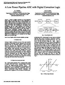
1. INTRODUCTION High-speed low-power Analog-to-Digital converters (ADCs) are the critical building blocks for modem communication and signal processing systems. They are the interface between the analog and digital signal processing. Since the mid-1970s. ADCs have been widely designed using integrating, successive approximation, flash, delta-sigma techniques. More recently, there has appeare’d a new class of ADC with an architecture known as pipeline, which offered an attractive combination of high speed, high resolution, low power dissipation and small die size. The pipeline ADC, therefore, became the optimum solution for present low power applications, such as a wireless communication system [I]. Fig 1 shows a typical pipeline scheme. A number of stages compose the structure. Each stage provides a mihit digital output code and a residual voltage. The next stage processes the residual voltage, performs digital conversion and gives another residual voltage. The output of the entire system comes from the bits generated by each stage. Due to the fact that the dynamic range of the residual voltage is smaller than the input by a factor of 2”, many architectures foresee an amplification of the residual voltage by the same factor to keep the dynamic range constant along the pipeline design [21. In general, ADCs require higher power consumption and circuit complexity than Digital-to-
P,ydmr*”