13-2 A 1.8V Single-Inductor Dual-Output Switching Converter for Power Reduction Techniques Dongsheng Ma, Wing-Hung Ki, Chi-Ying Tsui and Philip K.T. Mok Integrated Power Electronics Laboratory Department of Electrical and Electronic Engineering The Hong Kong University of Science and Technology Clear Water Bay, Hong Kong SAR, China Tel: (852) 2358-8535 Fax: (852) 2358-1485 Email:
[email protected]
Abstract A 1.8V integrated single-inductor dual-output boost converter is presented. This converter adopts a timemultiplexing control in providing two independent supply voltages using only one l p H off-chip inductor. The topology could easily be extended to give multiple outputs. The converter is fabricated with a standard 0.5pm CMOS n-well process. At an oscillator frequency of 1 MHz, the conversion efficiency reaches 88% at a total output power of 350mW.
multiplexing (TM) control, a single controller is shared by all the outputs. Synchronous rectification, in the sense that the transistor in replacing the diode is switched off when the inductor current tends to go negative, is employed, thus eliminating diode drops and enhancing efficiency. All power switches are fabricated on-chip and with only one inductor for two outputs, off-chip components are minimized. Other features include modified current sensing technique and ringing suppression technique, to be discussed in due course.
II. SIMO Converter Architecture and Control Strategy I. Introduction For a digital signal processor, high speed computation requires a high supply voltage v d d for fast switching. Since power consumption is proportional to the square of V, it is advisable to lower v d d when the computation speed could be reduced. Supply voltage scheduling using multiple or variable supply voltage schemes [I-51 are thus desirable in optimizing the power and speed of switching systems. A critical issue in implementing such a power management system is to generate multiple power supply voltages efficiently. Conventional solutions may use several independent converters or employ a transformer with multiple secondary windings to deliver energy into the various outputs [6,7]. The first method is not preferred because it requires too many components (controllers and power devices). The second method may suffer serious problems arise from cross regulation. A multiple-output converter with multiple inductors is reported in [5] recently. Because existing monolithic magnetic technology cannot fabricate inductors of suitable values and quality for efficient power transmission, inductors remain as off-chip components. As the number of outputs increases, the number of inductors increases accordingly, which is not preferable for portable applications. Furthermore, the topology in [5] limits to step-down conversion and only voltages lower than the power supply could be generated. If no high supply voltage is available, the system may not fulfill optimization tasks [3], because part of the system may have high speed requirements. Moreover, to work at low voltages, sophisticated analog circuits are needed, which are not easy to design. Hence, a boost converter is more favorable to power high-speed processor cores with a very low supply voltage. In this work, we introduce a single-inductor multiple-output (SJMO) boost converter topology. By employing time
137
4-89114-014-3/01
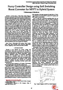
Fig. 1 shows the power stage of the proposed singleinductor dual-output (SIDO) boost converter. The two outputs Vo, and Vob share the inductor L and the switch SI. Fig. 2 shows the timing of the converter. It works with two complementary phases $a and 4. During Qa = 1, Sb is opened and no current flows into Vob, while SI is closed first. The inductor current IL increases until DlaT expires (determined by the output of an error amplifier), where T is the switching
p
r"""ipo L
Fig. 1 Power stage of the SIDO converter
:
S.
:wit
:H ;-n=
:
..
..
..
..
..
n. :
..
..: : .. . ... .
...
..
..
..
..:
Fig. 2 Timing diagram of the SIDO converter
2001 Symposium on VLSl Circuits Digest of Technical Papers
period of the converter. During D2,T, SI is opened and Sa is closed to divert the inductor current into the output Voa. A zero current detector senses the inductor current, and when it goes zero, the converter enters D3,T, and Sa is opened again. The inductor current stays zero until &, = 1. Here, DIa, DZaand D3a satisfy the requirements that
During &, = 1, the controller multiplexes the inductor current into the output Vob in similar fashion as discussed above, and the two outputs are regulated by the controller alternately. The presence of D3,T and D3bT puts the converter into DCM (discontinuous conduction mode), essentially isolating the control of the two outputs such that load variation in one output does not affect the other. Therefore, the problem of cross regulation is alleviated. Another advantage of DCM control is simple compensation of the system because there is only one LHP pole in the transfer function of the loop gain of each of the output [8]. With similar time multiplexing control, the converter can easily be extended to have N outputs as shown in Fig. 3, if N non-overlapping phases are assigned to the corresponding outputs accordingly. A switching converter with a similar topology was reported in [9] while the proposed converter was being fabricated. However, synchronous rectification is not employed, and power diodes are added in series with SIand Sz to prevent the inductor
fVK S.
F
* P
N
T
l
1
Table 1 summarizes and compares the features of the representative designs on N-output converters: TABLE 1: Comparison of multiple-output converters N converters
inductors power devices control loops
N 2N N
Ref. [5] Ref. [9] Thi work N 1 1 2N 2N+1 N+1 * 1 1
*No control loop is discussed in [9].
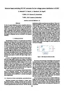
111. Controller and Functional Blocks A. Controller
Fig. 4 shows the block diagram of the single-inductor dualoutput boost converter. The two output voltages are scaled and fed to their respective error amplifiers. During $a = 1 , the switch SIis closed and the output voltage of the error amplifier EA, is sampled by the PWM generator to determine the duty ratio DIafor the output VOa.During = 1, the switch S2 is on and switch SI is off. In similar fashion, the duty ratio Dlb for Vob is determined. Note that many of the functional blocks in the control loop are time-shared that reduces the complexity of the controller.
B. Synchronous Rectification
TTT
***
current from going negative. Besides almost doubling the number of power devices, addition of the diodes lowers the efficiency significantly and deems unacceptable for low voltage applications. Moreover, according to the timing diagrams in [9], the converter works at the boundary of CCM (continuous conduction mode) and DCM. To maintain this condition, a load change at one output would increase or decrease the switching period, thus affecting the other output. Hence, serious cross regulation sets in and the design of the controller becomes very complicated, and no such working controller has been reported so far.
Fig. 3 Topology of SIMO converter with N outputs
For a switching converter, one of the switches is usually replaced by a diode, to save control circuitry and to block
Cumnt Sensor A
Scaler
PWM Generator
Scaler
-
V*
Over Current Delector Current Sensor B
Fig. 4 Block Diagram of SIMO Converter
2001 Symposium on VLSl Circuits Digest of Technical Papers
138
reverse current automatically. Now, imagine the switches Sa and Sb of Fig.1 are replaced by diodes with the anodes connected to the inductor. Without using switches, the inductor current cannot differentiate between V,, and V,b and will charge up both outputs at the same time and gives v,, = Vob in the steady state. This is the reason why a transistor is added in series with each of the diode in [9]. In order to achieve a high efficiency, synchronous rectification is adopted in this work. For implementation, free wheeling diodes are replaced by transistors M,, and Mpb with low on-resistance. Two current sensors A and B sense the currents flowing into the outputs V,, and V,, respectively. Consider the case for $, = 1. Because the converter works in DCM, the inductor current tends to go negative at the end of D,T. The bi-directional switch M, cannot block reverse current as a diode does, and when current sensor A detects a zero inductor current, the power transistor Mp is then turned off to prevent the current from flowing back to the source. Similar action applies to switch Mpb. The present design uses PMOS power transistors to replace the diodes. For a boost converter, the two output voltages are both larger than the supply voltage. The substrate of the switches and the supply voltage of the dead-time control buffer should be connected to the highest voltage of the system so that the switches can be fully turned on and off.
(with V,,, = 1 at the same time), M7 is also turned on with Vd, 2 0. In this case, Ms and M, have the same DC voltage biasing. Therefore, the current through M S is proportional to that of M, according to the scale ratio a = (W/L)s/(W/L),. M 5 is designed to be much smaller than M,, and CL