MVA '96 IAPR Workshop on Machine Vision Applications. November. 12-14, 1996, Tokyo, Japan
TMPSXST 1M: A Configurable Binary Morphological and Template Matching Processor Yudi Yanuhardi, Trio Adiono, and Tati L.R. Mengko Design Laboratory, Inter University Center on Microelectronics Institute Technology of Bandung Ganesha 10 Bandung 40132 - I n d o n e s i a Phone. 62-22-2506280, Fax. 62-22-2508763 Email:
[email protected],
[email protected]. itb.ac.id
Abstract
Using two processors, configured in parallel, the chip has been tested to perform various types of
A configurable chip for binary morpholpgical and temolate m a t c h o~erationsis presented here. The chip was designed based on FPGA design methodologies and fabricated in 0.8 ,um CMOS Gate Array technology. The TMPSXSTIM is able to process maximum 1024x1024 pixels binary image with 5x5 template size in a speed of 200 ns per pixel at I0 MHz clock rates. Two or more processors can be configured into 4 parallel confi-atrationsmake this processor able to perform a broad range of morphological and template matching operations.
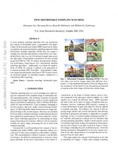
1 Introduction The TMPSXSTIM is a configurable processor for binary morphological and template matching operations. The chips are shown in Figure 1. The main processing unit of the TMPSXSTIM consists of array of processing element implemented in semi systolic architecture [I]. Sixteen templates can be downloaded into the processor at once, so template replacement can be done very fast. The processor has two image buffers as a source and destination buffer. The data are written and read from image buffer using asynchronous handshaking protocol. Processor's configuration and operation are controlled by setting its instruction registers. The processor can be configured into six parallel configurations, make it enable to perform a broad range of morphological and template matching operations. The prototype of processor was designed in the FPGA technology and done in the schematic level. The design requires 10.000 logic gates to implement all processor architecture. After verification steps, the design is transferred into 0.8 ,um CMOS Gate Array technology. Using this technology, processor performance can be improved to 10 MHz clock rates.
Figure 1 TMPSXSTlM Chips morphological image processing operations such as erosion, dilation, thinning, pruning, opening, closing, etc.
2 Processor Architecture The processor consists of seven main blocks, that are line delay circuit, processing unit, ternplateldon't care buffers, output mode, switch matrix, image buffer controller, and instruction registers. There are also several input-output ports as illustrated in Figure 2. These blocks perform the following functions:
+ Line Delay Circuit Line delay circuit is used to generate 5 by 5 neighbourhood data for the processing unit. Data input come from the source image buffer in raster scan format. Line delay circuit consists of four 25 1-bits internal FIFO buffers that can be used to process maximum 256x256 pixels image size. For larger image size, it must use external FIFO buffers that consist of two 1024x4-bit bidirectional RAMS. The line delay circuit also supply delayed image data for the output mode block.
+ Processing Unit Processing unit consists of 105 processing elements configured in semi-systolic array architecture in which similarity measurement between template and image is determined. Similarity measure (SM) between template g and image fin image area A can be expressed as [I]: with: f ' and g ' are complement of f and g respectively. The similarity-measure is controlled by setting an appropriate value to the thresholder element.
+ TemplateIDon't
Care Buffers Sixteenth 5x5-pixels templates can be stored in templateldon't-care buffers at once. Template selection is done by the instruction register. Smaller template size is enabled by inserting don't care data in don't-care register.
+ Output Mode Output mode is used to select a combinational function (AND, OR, XOR, difference, etc.) between processed data, delayed (original) data, andlor output data from other processors, or just pass one of them without any combinational function. Output mode consists of seven modes for single processing operations, nine modes for parallel processing operations, and one mode for parallel thinning operation. Output mode selection is done by the instruction register. Switch Matrix Switch Matrix is used to control data flow at image buffers, transfer inlout ports, data-monitor port, and parallel port. Switch matrix is also used to
determine which data will be send to the line delay circuit, from image buffer or from parallel port (in the parallel mode).
+
Image Buffer Controller Image buffer controller is used to control readwrite process in the image buffers, that is as a source or destination buffer. This controller also has responsibility to distribute enable signals to the line delay circuit and to the processing unit.
+
Instruction Registers Instruction registers are used to configure and to control the operation of the processor. Configuration registers consist of nine 8-bits registers. Using an additional address decoder, they can be accessed by a PC. Data transfer between processor's buffers and external devices is done by using asynchronous handshaking protocol through the transfer inlout port. There are three handshake lines and one data line. Transfer process is initiated from the processor by its busy and request signals. The data-monitor port is used to monitor processed data or difference between delayed and processed data for further processing. This features are useful in thinning (to monitor convergence), template matching operations (to monitor patterns' locations), etc.
3 Parallel Processing Features TMPSXSTIM has four parallel modes as illustrated in Figure 3. From these modes, the processors can be
Figure 2 Processor Architecture
MODE 1
MODE 0 SLAVE
MASTER
SLAVE
MASTER
1 M
U O
< l 1 1 dl i
M
i
& S P U J ~, O M
id--.
I , , I
I D
DE 2
MODE 3 SLAVE
MASTER
MASTER
SLAVE
r
I
s11 W M P U ' = O M + ~
+
;;
I
I
MPU] rSpU1
1
C
HD
Master Processing Un~t Slave Processing Unit
[OM]
D
ID
Output Mode
3 Swltch Matnx
[G] Source Image Buffer
Unused Path or Block
101 Destinat~onImage Buffer
Figure 3 Parallel Modes of TMPSXSTIM configured into six parallel configurations as can be seen in Table 1. In each parallel mode, one processor has to be defined as a master and another processor(s) as slave. The master processor will generate synchronisation signal to the slave processor(s), so two or more operations can be done simultaneously. Together with the output mode block, these features make the processor have capability to perform a broad range of morphological and template matching operations. This mode also supports parallel thinning operations, as described in [2], in which three processors running in parallel.
4 Design Implementation and Performance The chip has been fabricated in 0.8 pm CMOS Gate Array technology and verified to work at 10 MHz clock speed. At this clock speed, processor's data output rate is 5 Mbits data per second. The detailed specifications are shown in Table 2. The design prototype consists of two TMP5X5TlM chips that can be operated in parallel configurations. The processor operations are controlled by a PC and binary image data is provided by a frame grabber. Data transfer between the image processor and PC is performed by an asynchronous handshaking protocol. In addition, a data-monitor chip was designed to monitor the process convergent and other monitoring tasks that related to the process being observed. The prototype has been tested for various morphological
and template matching operation, and now it is used in the path planning research [3].
5 Conclusion A new processor architecture for morphological and template matching operations has been described in this paper. The processor was fabricated in 0.8 pm CMOS Gate Array technology and has capability to process maximum 1024x1024 pixels binary image with 5x5 template size in a speed of 200 ns per pixel at 10 MHz clock rates. Two or more processors can be configured into six parallel configurations make this processor able to perform a broad range of morphological and template matching operations. For future development, a work will be done to design a job sequencer chip to control the processors' operation, instead of using a PC, so processor configuration time will be reduced.
6 Acknowledgement Part of this research funding was provided by the National Development Planning Agency under RUT project. The authors wish to thank to Ir. Mervin T. Hutabarat, MSc., Ir. Indrajit Dimyati, and Lafin for their continues support to this research.
Table 1 Parallel Configurations of TMPSXSTI M
I
I
Master
I
Slave
1
Source
I
Destination
I
I
Outout Mode
Table 2 Processor Specifications
References [I] Djunatan, Matias, "Processor Architecture Design for Binary Morphological and Template Matching Operations", Final Project Report, Institute Technology of Bandung, February 1991. [2] Jang, Ben-Kwei and Roland T. Chin, "Analysis of Thinning Algorithms Using Mathematical Morphology", IEEE Trans. on PAMI, Vol. 12, No. 6, p. 541-55 1, June 1990. [3] Adiono, Trio et all, "Binary Template Matching Solution to Path Planning Problem", ACCV'95, Singapore, 1995 [4] Adiono, Trio et all, "Design and Implementation Prototype of Binary Template Matching Processor Based On Logic Cell Array", ICM '94, Istanbul, 1994. [5] Yanuhardi, Yudi and Tati L.R. Mengko, "Design and Implementation of Configurable Binary Template Matching Processor for Morphological
and Template Matching Operations", ICME'96, Bandung, Indonesia, 1996. [6] Jain, Anil K., "Fundamentals of Digital Image Processing", Prentice Hall International Inc., Singapore, 1989. [7] P.P. Jonker and R.P.W. Duin, "Consideration On A VLSI Architecture For Cellular Logic Operations", IEEE, 1990. [8] P.P. Jonker, "Morphological Image Processing Architecture And VLSI Design", Kluewer Techniche Boeken B.V., 1992.