A Low-Power Microcontroller with On-Chip Self-Tuning Digital Clock-Generator for Variable-Load Applications Mauro Olivieri Univ. of Rome La Sapienza,
[email protected]
Alessandro De Gloria, Univ. of Genoa,
[email protected]
Alessandro Trifiletti Univ. of Rome La Sapienza,
[email protected]
Abstract Clock disabling for power management has been implemented in some microcontrollers, but the wake-up time of Xtal/PLL-based systems is incompatible with fast interrupt response. On the other hand, hardwired on-chip clocking has been used for dedicated circuits. We illustrate the design issues of a general-purpose microcontroller core with a programmable on-chip fullydigital clock generator. The CPU is compatible with the PIC16C57 instruction set and supports softwarecontrolled clocking modes – ranging from 44 MHz up to 124 MHz; on-line self-tuning of the maximum full-speed frequency in case of peak-performance requirements; ultra-fast wake-up even with totally disabled clock generator – namely 8.6 ns. 1. Introduction Low power consumption in embedded systems has become a key factor in many applications, and is going to represent an increasingly important issue. Portable applications, needing long battery life together with high peak-performance, are demanding a very careful design at all levels, from the cell library and layout strategy of VLSI chips up to the architecture and even the software layers of the system. Microprocessor-based portable applications, in particular, often have a varying computation load, frequently dominated by idle periods. Examples in this field are security-alarm systems, personal communications systems, personal organizers, automotive embedded control systems and others. While software can do a notable part in optimizing the use of the microprocessor system resources with the view of lowpower consumption, it is essential that the microprocessor architecture supports specific features to exploit the characteristics of the application in order to reduce the consumed energy or power. Existing microprocessors, especially in the category of microcontrollers, often have the capability of partially gating the clock signal when they fetch and execute a NOP instructions or other minimal-activity instructions [1], or when a peripheral can be powered-down, but this does not totally eliminate spurious power consumption in case of relatively long idle periods. Other processors can enter low-power operating modes, disabling the clock signal generator (Xtal oscillator and PLL). However, this is not totally efficient in the important application cases
that require a fast response to an external signal after an idle period, because the time to recover from a totally idle state is often several µs, due to oscillator and PLL transient. On-chip clocking, based on application-specific hardwired oscillators, has been proposed to avoid the power consumption of an external oscillator [2,3,4], or to realize very fast sequential specialized operations, such as arithmetic algorithms [5] or DSP dedicated functions with fixed cycle count per sample [6]. Fast wake-up from idle mode and self-tuning of the maximum frequency in complex architectures are an interesting novel target of on-chip clocking design. We illustrate the design issues of a general-purpose microcontroller core with on-chip fully-digital clock generator. The designed CPU is compatible with the PIC16C57 instruction set and supports softwarecontrolled clocking modes – ranging from 44 MHz up to 124 MHz, ultra-fast wake-up from low power modes even with totally disabled clock generator – namely 8.6 ns, and on-line self-tuning of the maximum full-speed frequency in case of peak-performance requirements. 2. Design overview We developed our work on the basis of PIC16C57 instruction set architecture. Starting from a structural gate-level VHDL netlist of the microcontroller, we introduced a novel digital clock generator, clock distribution system, and clock tuning architecture. The project involves several design levels, from the circuit design of the clock generator to the logic design of the frequency control unit, to the architecture level design of a maximum frequency tuning system as well as the interaction with software machine-code instructions. The underlying assumptions to our approach are that FREQUENCY 0
IDLE
f0
. . .
REDUCED POWER FREQUENCIES
f7
VALUES f8
. . .
f15
POSSIBLE FULL-SPEED FREQUENCIES
Fig. 1 – Summary of the operating modes. Actually fi = 1/(T0 – iT) , where T0 = maximum cycle time of the oscillator and T = minimum cycle time quantization.
on-chip checking mechanism. The reduced-power mode is itself divided into a set of 8 cycle time values, from the longest produced by the programmable oscillator to the shortest allowed by the CPU architecture under worstcase CMOS technology conditions. This is useful when the microcontroller must operate at a low computation rate, so that it would be forced to repetitively enter and exit the idle mode (requiring an interrupt) if it operated at full-speed. A summary of the operating frequencies is illustrated in Fig. 1. The mechanism for passing from one mode to another
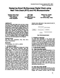
Microprocessor core
R O S C
FSM OSC
OSC
Fig. 2 – Logical view of the clocking system
Table 1 – Transition mechanisms between different operating modes next mode full speed red. power idle present mode full speed software software red.power software software software idle not allowed interrupt -
the processor design is implemented with a fully static standard cell library, and that it is possible to identify the register-to-register critical path of the microarchitecture design. Both assumptions are easily met in a standard semi-custom design environment. At the functional level, we introduce three operating modes corresponding to clocking system states, namely full-speed, reduced-power, and idle. The idle mode corresponds to stop the programmable on-chip oscillator. The full-speed mode corresponds to automatically setting a clock cycle time which is self-tuned on the maximum speed allowed by the CPU architecture, by means of an
IR
is summarized in Table 1 (transition from the reducedpower mode to the same mode is intended as a frequency change). The external interrupt mechanism activates on
Program memory
Q4 Q1
Stack
Q4 PC
Decoder
R Q4
Q2 R
F S R
Q2 Q3
Aluop ALU
R
From IR
Q4 W
Status
MUX
MUX
R
R
Q2
Reset Clocker
Q2
Q4
Q1 Q2 Q3 Q4 CLK
Data memory
WDT
Fig. 3 – Global view of the microcontroller architecture
Wake-up
any hardware interrupt or reset signal arriving at the processor when it is in idle mode. The clock frequency is set to the highest value in the reduced-power frequency range, i.e. f7. The software mechanism activates by writing a register chosen from the available register set of the PIC architecture. A specific issue of an on-chip clocking system is the synchronization with on chip peripherals/memory and with the external bus. In our microcontroller all the on-chip peripherals including instruction and data memories are synchronous with the main clock, and the communication the with external environment is obtained only by asynchronous I/O ports. For the implementation phase, we referred to a 0.8 µm static CMOS library. 3. Architecture and clock design Fig. 2 shows a global logical view of the clock subsystem with the CPU core. The frequency of the oscillator is programmable by means of the 4-bit number contained in the dedicated register r_osc. The register is directly driven by the state machine fsm_osc, that manages both the transitions between clocking modes and the automatic tuning of the frequency according to the actual critical path delay in the microarchitecture. The CPU core microarchitecture is detailed in Fig 3. All the modules have been synthesized from VHDL. Note that the PIC architecture is based on a 4-phase timing
scheme, where the four non-overlapping clock phases, namely Q1, Q2, Q3 and Q4, are generated from the main clock by a dedicated unit (clocker). Actually the whole architecture cycle time is therefore composed of four oscillator clock cycles. Table 2 reports a list of the critical delay of the architecture modules, resulting from prelayout critical path extraction, including parasitic estimation. In our implementation, the ALU module has the longest delay and represents the limit to the cycle time. Table 2 – Propagation delay and gate count for the proposed microarchitecture
Functional block
Cell count
Alu Decoder Register file Stack I/O control
192 182 1400 136 50
Propagation delay (ns) 7.9 7.2 5 3.2 2
By writing an integer number in the five least significant bits of the register 20H (that we call R20), three of which are directly copied into the register r_osc, the software program can interact with the state machine fsm_osc Nop opcode
Normal operand
Q2
To decoder IR
00000000
Test operand
11111111
00000000 00000001
Program memory
Q4 ALU
Normal operand
PC
Q1
Normal PC address
Test operand
Q2 Q1 Q2 Q3 Q4
Test operand control
Tuning mode
Clocker
Force NOP
CLK Osc
S FSM OSC
4
R
R osc 4 Q1 Q2 Q3 Q4 4
4 Reg 20H
INT
Fig. 5 – Detail of the architecture design to support the frequency tuning mechanism
according to the following rules: • R20 (0 to 2)