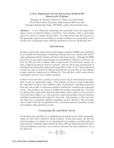
A Robust Commutation Circuit for Reliable SingleStep Commutation of the Matrix Converter S.A. Nabavi Niaki and R. Iravani
H. Kojori
Department of ECE, University of Toronto Toronto, ON, M5S 3G4, CANADA
[email protected]
Honeywell Advanced Technology Mississauga, ON L5L 3S6, Canada
Abstract—The matrix converter (MC) is an attractive topology for the more electric aircraft because of its high-power density and bidirectional power flow features. One of the challenging issues in MC is the current commutation. The commutation process in a matrix converter (MC) is more complex as compared with that of the traditional AC-DC-AC converter due to the lack of natural free-wheeling paths. Multi-step commutation methods along with various voltage clamp circuits, connected at input and output, have been proposed for the MC. These methods are complex and require accurate real-time information about direction of current and input AC system voltages. Reducing the commutation time and process is a main objective of using MC in aerospace applications where the range of frequency is between 360-800 Hz. This paper presents a robust commutation circuit for reliable single-step commutation of the MC, and demonstrates its feasibility through computer simulations and experimental results obtained from a laboratory scale prototype.
I.
INTRODUCTION
The matrix converter (MC) has attracted significant attentions [1]–[8] due to its features that enable (i) adjustable power factor, (ii) bi-directional power flow, (iii) high-quality waveforms, and (iv) compact design due to the lack of energy storage components.
four to two [14] or one [15]. This, hence, increases the commutation algorithm complexity. For the aerospace applications where the range of inputside frequency is between 360-800 Hz, reducing the commutation time is one of the main objectives. This paper introduces a novel single-step commutation circuit for the MC that provides a safe and reliable bidirectional path for the load current during the commutation period and protects the switches against any overvoltage due to the load current interruptions under steady state or fault conditions. This commutation circuit is directly connected across each switch module and does not require an additional clamp circuit. The main advantage of the proposed commutation circuit is that it introduces only a fairly short deadtime delay (in the range of nanoseconds). This single-step delay considerably minimizes the commutation time compared to multi-step commutation methods. The proposed method does not require line current and/or phase voltage measurements. II.
MULTI-STEP COMMUTATION PROCESS
(i) The sequence of switch turn on-off is determined by the direction of output current and/or the values of the input-side voltages. The commutating reliability depends on accurate evaluation of the voltage difference of the two involved input phases and the output-side current direction. When the outputside current or the difference of the input voltages is small, the commutation is prone to failure.
During the past decades, three kinds of multi-step commutation strategies have been proposed, i.e., 1) currentbased commutation (CBC), 2) voltage-based commutation (VBC), and 3) hybrid commutation (HC). The multi-step commutation algorithms require line current and/or phase voltage measurements. CBC and VBC strategies rely on the knowledge of the output-current direction and the relative magnitude of input voltages respectively. However, the directions of output current and the relative magnitudes of the input voltages are difficult to measure, particularly at zero or close to zero crossing instants. The misjudgment of outputcurrent direction in the commutation process leads to an open circuit of the load current and causes overvoltage. If the relative magnitude of the input voltages is misjudged, a short circuit of the input phases can happen. HC strategies rely on information about the relative magnitude of input voltages and the output-current direction.
(ii) Reducing the commutation time enhances the quality of the input and output waveforms [13]. The commutation time can be reduced by reduction of the number of steps from
Fig. 1 depicts the 4-step sequence of current commutation from the bidirectional switch Sa (AC switch module) to the bidirectional switch Sb, when the load current is positive
Various multi-step commutation strategies for the MC have been proposed [8], [10] and compared in the technical literature [11],[12]. Among these methods, the 4-step commutation is the most widely accepted one. The main technical issues of the multi-step methods are as follows.
978-1-4799-2325-0/14/$31.00 ©2014 IEEE
3349
(IL>0), e.g., towards the load. This commutation strategy is based on CBC and the commutation sequence is as follows: Commutation Circuit
t < t1;
Sa1 and Sa2 are on
t = t1;
Sa2 turned-off , Sa1 conducts (load current)
t = t2;
Sb1 turned-on , both Sa1 and Sb1 conduct
t = t3;
Sa1 turned-off , Sb1 conducts
t > t4;
Sa1 vb
+
va
iCb +
Sb1
Sb
Sa2
IL
Sb2
vb
vCb
vL
iL
+
Lb
ib
+
Sb
Fig.3 A two-to-one switching configuration with the commutation circuit.
Sb1 Sb2
A. Pre-commutation (Sa closed, Sb open) Initially, the switch in phase a (Sa) is closed and the load is supplied by va, i.e., iL = ia and ib = 0. The load voltage and the voltage across Sb are
t1
t2
t3 t4
vL va La
PRINCIPLES OF OPERATION OF THE PROPOSED COMMUTATION CIRCUIT
The basic components of the proposed commutation circuit, Fig.2, are 1) a diode bridge, 2) a capacitor, and 3) an energy mitigation circuit (EMC). The function of EMC is either to dissipate the stored energy in the capacitor through a resistive component or to return the stored energy back to the system [17].
C
Sa1 Sa2
The commutation time of 3.6 μs is reported in [8] for safe commutation and the minimum reported commutation time is about 1s [16].
SM
Sa
Cb
Sb1 and Sb2 both are on.
Fig.1 The 4-step sequence of current commutation from bidirectional switch Sa to bidirectional switch Sb when the load current is positive (IL > 0).
III.
Ca
Sa
va
vCa
La
ia
t = t4; Sb2 turned-on to allow negative current conduction
+
iCa
dia , dt
v Sb v b v L , v b v a La
(1)
di a dt
(2)
Equation (2) is valid if the diode bridge in phase b is blocked by vCb > vba, assuming the load current ia during the short period is constant, i.e., dia/dt = 0. Otherwise the bridge conducts and the voltage across Sb is vCb. To satisfy this condition, the commutation capacitor voltage should be more than the line-to-line voltage, i.e., |
|,
, ∙
(3)
B. During-commutation (Sa open, Sb open and then closed) For this condition, the commutation process can be investigated in two stages: 1) the load current transfer from Sa to the commutation circuit of phase a (turn-on delay), and 2) the load current transfer from the commutation circuit of phase a to switch Sb after closing Sb (transition delay).
EMC
Fig.2 The proposed commutation circuit for MC and its basic components.
To explain the concept, a two-phase to one-phase MC, Fig. 3, is adopted. The commutation circuit is connected across each main switch and provides a bidirectional path for the load current by introducing a turn-on delay during the commutation process. The analysis also considers the effect of line (stray) inductance. The commutation process includes (i) opening the outgoing switch, (ii) transferring the load current to the commutation circuit, and (iii) closing the incoming switch after the turn-on delay, as follows.
1) Turn-on delay (Sa open, Sb open) Switch Sa is turned off and Sb is turned on. Since the turnon delay strategy is adopted for the safe operation of switches, Sb is turned on after time delay td. Upon Sa turn-off instant, the load current flows through the commutation circuit; i.e., iCa = iL = ia and va continues to supply the load. The load current flows in the commutation capacitor (Ca) and charges the capacitor
vCa vCa0
1 C
i dt, td
a
(4)
where vCa0 is the capacitor initial voltage. Since the diode bridge across Sa is open and conducts the load current, the capacitor voltage appears across Sa, i.e.,
3350
v Sa vCa
(5)
The positive/negative sign in (5) depends on the positive or negative direction of the load current, respectively. In the following, we consider the positive current direction unless otherwise specified. The voltage across the load and Sb are
v L v a La
dia vCa , dt
v Sb vb va vCa La
(6)
dia dt
(7)
2) Transition delay: Transition from commutation circuit of phase a to switch Sb (Sa open, Sb closed) After the turn-on delay (td), Sb is closed. However, because of La and Lb, the current cannot be instantaneously transferred from phase a to phase b. The capacitor in bridge-a conducts until its current goes to zero. This transition interval depends on the line (stray) inductances La and Lb. Under this condition both va and vb contribute to the load current, and
vL
di di 1 (v a vb La a Lb b vCa ) 2 dt dt
(8)
When the bridge of phase a is conducting, the voltage across Sa is Vca. For a symmetrical system where La = Lb, the rates of change of currents ia and ib are the same, but the current directions are different and thus the differential terms in (8) cancels out. 3) Post-commutation (Sa open, Sb closed) In the post-commutation period, the load current is fully transferred to phase b and the diode bridge in phase a is blocked by vCa. The conditions for this period are 1) vSb = 0, 2) ib = iL, 3) ia = 0, and the load voltage and the voltage across Sa are
vL vb Lb
dib , dt
v Sa va vb Lb
B. Switch voltages and overvoltage protection The switch voltages are expressed by (2), (5), (7), and (10) for all operating intervals. Equation (7) provides the maximum switch voltage of vba+vCa (line-to-line voltage plus the commutation capacitor voltage) when the differential term is ignored. However, (3) indicates the diode bridge is open and Sb voltage is vCb, and not vab+vCa. This is exploited as the overvoltage protection criteria for the switches. Therefore, by maintaining the capacitor voltage level above the natural commutation voltage, the maximum switch voltages can be determined.
dib dt
VCa
+
(9)
Va
(10)
COMMUTATION CIRCUIT PERFORMANCE
The main feature of the commutation circuit is to provide an auxiliary path for the load current during the commutation period when all the switches are open. During this period, the load current charges the commutation capacitor and the switch voltage is same as the capacitor voltage. Since the same gating signal is applied to both switches in the AC switch module (Fig.1), the number of gate drivers can be reduced to half as compared to the other multi-step approaches.
ia V L
VSa
La
Sa
115 Vrms 400 Hz
It should be noted that the actual delay in the proposed system is only td and the next gating signal can be updated after td which is in the range of hundred nanoseconds. Performance of the commutation circuit in the following sections is investigated based (1) to (10). IV.
A. Energy Mitigation Circuit (EMC) The performance of the commutation circuit highly depends on the duration of the turn-on delay (td). During these periods, the line current charges the commutation capacitor. The capacitor voltage is governed by (4). If there is no auxiliary path (circuit) to discharge the capacitor, the capacitor voltage increases based on (5) and (7). An energy mitigation circuit can be employed to regulate the commutation capacitor voltage. The average power rating of an EMC is less than 3 percent of the total average power rating of the unit, depending on the type of switching devices, duration of deadtime and turn-on/turn-off delay compensation for the switching device PWM gating-pattern. The energy stored in the capacitor can be either dissipated in a resistive component or returned to the system depending on turn-on delay (td), the unit rating, and the cost justification. For low power applications, the collected energy during commutation can be dissipated in a resistor. However, for a larger unit, an energy recovery circuit can be employed to return the stored power back to the system.
0.1 1 mH
Fig.4 Study system for the overvoltage analysis.
Fig.4 provides more insight into the MC overvoltage issues. An inductive load is selected as the worst case scenario. When Sa is closed ,
(11)
and when Sa is open ∙
(12)
In (11), the dominant voltage component across the load is Va while in the (12) is (Va-VCa). Since Vca is greater than Va (condition of (3)), the load voltage is negative and the current decays to zero. Fig. 5 shows the voltage waveform based on time-domain simulation of the system of Fig. 4. At t=0.076s,
3351
Sa is opened and d the line curren nt is diverted to o the diode brid dge annd the commu utation capacito or (Ca). At thiss time instant, the brridge is open, the load voltaage (VL) becom mes negative and a foorces the load current c to zero o. At zero curreent (after 200 s), thhe bridge is closed and ia =0, VL=0, and VSa=V = a.
(a)
The simulatiion results sho ow that the fulll load current can bee successfully interrupted i by the commutatiion circuit with hout ovvervoltage acro oss the main sw witch.
Gaating siggnal
(b)
C
SM
vC_set_Hig
SA
(a a)
R
vC
vC se set Low
(b b) Fig.6 a) C Commutation circuuit Type-1 and b) Commutation circcuit Type 2a
(cc)
The advantage of this connfiguration is that the commuttation capacitoor is dischargedd through the E EDC during the turnn-on period andd provides zeroo voltage and zzero current conditioons for the maiin and the auxxiliary switchess at turn-off instant, respectively.
200 s (d d)
Tim me (s)
vCa (V)
Fiig.5 Simulation results for the system m of Fig. 4: a) capacitor voltage, b) load l current, c) loaad voltage, and d) AC switch voltagee.
V.
650
620
A. Type-1Comm mutation Circu uit Fig.6.a show ws the Type-1 circuit, c where SM is the main AC A sw witch and SA iss an auxiliary switch s for the energy e dissipattive ciircuit (EDC). The T main featu ure of this circu uit is its capabiility too fully discharg ge the commu utation capacito or before the next n coommutation process takes plaace.
600
Type-1 conffiguration is sim mple and both the main and the auuxiliary switch hes are interloccked, i.e., the same gating sig gnal iss applied to botth switches. Du uring turn-on peeriod, SA is clo osed annd C is fully discharged d throu ugh R. When the t turn-off sig gnal iss applied to botth SM and SA (fo or example in phase p a in Fig. 3), thhe load curren nt is transferred d from the maain switch to the coommutation circuit of phase a. Since the commutattion caapacitor is fullly discharged, it provides neearly zero voltage sw witching durin ng turn-off. The T capacitancce size could be m minimized by permitting th he load curren nt to charge the caapacitor up to the t line-to-line voltage during g the commutattion peeriod, i.e.,
iL .t , v
where t = td and v = Vab.
(13)
vCa
630
Based on various contro ol strategies and EMCs, the foollowing enh hanced config gurations of the propo osed coommutation cirrcuit can be reaalized.
C
vC_set_High
640
ENHA ANCED VERS SIONS OF THE E PROPOSED D COMMUTAT TION CIRCUIT T
(a)
610
vC_set__Low 1..3
1.4
1.5
1.6
1.7
1.8
1.9 -3
x 10
iCa ((A)
(b)
150
Charrging during coommutation
100 50 0
Dischaarging by ERC
-50 -100
1..3
1.4
1.5
1.6
Time (s)
1.7
1.8
1.9
x 10 Fig.7 a) T The commutation capacitor voltage and b) current of pphase-a forr the circuit of Fig . 3 (Type-2.a. com mmutation circuit).
-3
B. Typee-2.a Commutaation Circuit The commutation circuit Type-22.a is shown inn Fig.6.b. In this connfiguration, thee commutationn capacitor is charged to more thhan the natural commutation voltage (vC_set__low). Hence the diodde bridge is bloocked by the capacitor voltagge when the main sw witch is off andd no current floows into the briidge at “on“
3352
orr “off” sate du uring the norm mal operation. However, durring coommutation, since s there is no path for the load curreent, exxcept through the commutattion capacitor, the load currrent oppens the diodee bridge and flows f through the commutattion caapacitor. Durin ng commutation n, the capacitorr is charged to the vooltage given by y (4), i.e. vC0 is equal to vC_set__Low. The energy y stored durin ng the comm mutation can be reecovered by an n Energy Recov very Circuit (E ERC) or dissipaated inn a resistive co omponent. For the sake of sim mplicity, the ERC E iss represented by b SA and R in n Fig.6.b. To recover r the sto ored ennergy during commutation and prevent overvoltage, the foollowing contro ol strategy is ap pplied to the au uxiliary switch:: - The capacito or voltage (vC) is monitored and compared d to the upper preeset value of vC_set_High . C - When vC beccomes greater than t vC_set_High, the “on” signaal is applied to th he auxiliary sw witch and the caapacitor energy y is transferred to o the ERC.
Type-2.a is chharged above the natural capacitoor voltage in T commuttation voltagee (line to linne voltage) suuggests the integratiion of all com mmutation cappacitors as onee capacitor. Fig.8.a shows the Tyype-2.b commuutation circuit (Integrated Capacitoor) for a MC w with n main AC C switches. In thhe Integrated C Capacitor MC (ICMC) conffiguration, a diode brridge is conneccted across eacch main switchh to provide a bidirectional path foor the load currrent during coommutation. The dc terminals of all diode briddges are conneected to the same dcc bus which is cconnected to oone commutatioon capacitor to form the integrated capacitor confi figuration. The basic circuit of a three-phase-to-one-phhase matrix converteer, including tthe IC, is shown in Fig.8.b. The main feature of this confiiguration is thhe load currennts can be divertedd to one singgle capacitor during the coommutation period, aand a hysteresiis control strateegy can be adoopted for the energy m mitigation circuuit.
- When vC beecomes equal or o less than vC_set_Low , the “o off” C signal is ap pplied to the auxiliary sw witch to stop the capacitor disscharge and to o maintain the capacitor volttage above the naatural commutaation voltage.
Source
Input Filter
Fig.7 show ws the commu utation capaciitor voltage and a cuurrent of phasse a for the circuit c of Fig. 3 based on the paarameters giveen in the Appeendix. In this analysis, a R is 8, 8 annd the threshold voltages in Fig.6.b F are: vC_sset_Low = 610 V and a vCC_set_High =650 V. V
(a)
+
Load
ICMC 3-1
dc d buses 20 kHz
Referencce voltagee
C
Gatting & Coontrol
S Switching F Frequency
Fig.9.aa) The three-phase-to-one-phase MC C parameters.
n moduless
(b)
Integrrated EMC Capacitor
Fig.99.b) Experimental 3-to-1 phase MC..
VI.
Fiig.8. a) Type-2.b commutation c circu uit (Integrated Capacitor), b) a three-phase-to o-one-phase ICMC C.
C C. Type-2.b Co ommutation Cirrcuit (Integrateed Capacitor) Commutatio on circuits Typ pe-1 and 2.a are designed for eaach AC switcch module. The fact that the commutattion
EX XPERIMENTAL VERIFICATION
To vverify the prooposed conceppts, a 2-kW, 33-to-1-phase ICMC was developeed and tested.. Details of S SIMULINK simulatiion model andd the corresponnding experimeental results are show wn in figures 9.a and 9.b reespectively. Thhe prototype
3353
w was designed to t accommodaate the input frequency in the raange of 360 to 800 Hz which suitablle for aerosp pace appplications and d provide controlled output voltage with the fixed frequency y of 400Hz. Six MOSFET T switches and d a Type2.b commu utation circuitt are used forr this setup. The T V Venturini modu ulation schemee [18] at 20 kHz k is adopted d to coontrol of the AC switched. Figure 10 co ompare the tim me-domain sim mulation resultss in SIIMULINK en nvironment and a the expeerimental resu ults coorresponding to the output voltage v and currrent, at the in nput phhase voltage off 35V at 800 Hz.
which aa) provides robuust and reliablee single-step coommutation to reduuce the comm mutation time, b) provides overvoltage protectioon for switchees, c) reduces device stress dduring turnoff andd turn-on proccesses, d) reduuces the numbber of gate drivers tto half, and e)) prevents degrradation of PW WM patterns by miniimizing the durration of deadttime. Technicaal feasibility and opperation of thhe proposed commutation circuit are investiggated through ccomputer simuulations and vvalidated by experim mental results oobtained from a laboratory scale threephase-too-one-phase IC CMC prototype. Simulation
Sim mulation
van (V)
(a)
vAK (V)
(b)
(a) (c)
vCa (V) Cap
(b)
(d)
iloaad (A)
Time (s)
Time (s)
Tiime (s) Experrimental
Experimental (a)
(a) (b) ((b) (c)
(d)
Fiig. 10. Simulation and experimental results of the system of Fig. 10, a) Output curren nt and b) output vo oltage (50 V/div, 1 ms/div).
Figure 11 compare c the siimulation and the experimen ntal reesults correspon nding to a high her voltage op perating conditiion, i.ee., Vin=117V rm ms, fin=800Hz, Iout = 2. 536A rms, and fout=4 400 H Hz. The close agreement a bettween the sim mulation and the exxperimental results verifies th he validity of the proposed MC M coommutation circuit. c The details d of the simulation and a exxperimental seetup for a 3-to o-3 ICMC, including the fiilter deesign (passive and active) an nd the energy mitigation circcuit w will be the subjeect of a subsequ uent paper.
Fig. 11 Siimulation and expeerimental results ffor the 3-to-1-phasse MC, a) inpuut voltage phase-aa (200V/div), b) vooltage across AC sswitch (20 0V/div), c) Inteegrated Capacitor vvoltage (200V/div), and d) outpput current (5A/diiv).
VIII. APPEN NDIX Systtem parameterss for simulationn results in Fig 3. va = 2300V, fa = 800Hz, vb =2330120V, fb =800Hz, td H, Ca = Cb = 5 F. = 100nss, La = Lb = 1H
VII. CONCLUSIONS O
Loadd: RL = 0.64, LL = 135H.
A review of commutation methods m for matrix converterrs is prresented and th he strengths an nd practical lim mitations hinderring diirect matrix converter c operration are highlighted. A new n siingle-step comm mutation for th he matrix conv verter is presen nted
A 5 0% pulse widdth with the peeriod of 50s (20kHz) is applied as the switchinng signals.
3354
IX. [1]
[2]
[3]
[4]
[5]
[6]
[7]
[8]
[9]
[10]
[11]
[12]
[13]
[14]
[15]
[16]
[17] [18]
REFERENCES
Arevalo, S.L., Zanchetta, P., Wheeler, P.W., Trentin, A., Empringham, L.: ‘Control and Implementation of a Matrix-Converter-Based AC Ground Power-Supply Unit for Aircraft Servicing’, IEEE Transactions on Industrial Electronics, 2010, 57, (6), pp. 2076 - 2084 Kolar, J.W., Friedli, T., Rodriguez, J., Wheeler, P.W.: ‘Review of Three-Phase PWM AC–AC Converter Topologies’, IEEE Transactions on Power Electronics, 2011, 58, (11), pp. 4988–5006 Rodriguez, J., Rivera, M., Kolar, J.W., Wheeler, P.W.: ‘A Review of Control and Modulation Methods for Matrix Converters’, IEEE Transactions on Industrial Electronics, 2012, 59, (1), pp. 58-70 Wheeler, P.W., Rodriguez, J., Clare, J. C., Empringham, L.: ‘Matrix converters: A technology review’, IEEE Transactions on Industrial Electronics, 2002, 49, (2), pp. 274–288 Dasgupta, A, Sensarma, P.: ‘Low-frequency dynamic modelling and control of matrix converter for power system applications’, IET Power Electron., 2012, 5, (3), pp. 304-314 Arias, A., Empringham, L., Asher, G.M., Wheeler, P.W., Bland, M., Apap, M., Sumner, M., Clare, J.C.: ‘Elimination of waveform distortions in matrix converters using a new dual compensation method’, IEEE Transactions on Industrial Electronics, 2007, 54, (4), pp. 2079–2087 Casadei, D., Serra, G., Tani, A., Zarri, L.: ‘Optimal Use of Zero Vectors for Minimizing the Output Current Distortion in Matrix Converters’, IEEE Transactions on Industrial Electronics, vol. 56, no. 2, pp. 326-336, Feb 2009. She, H., Lin, H., He, B., Wang, X., Yue, L., An, X.: ‘Implementation of Voltage-Based Commutation in Space-Vector-Modulated Matrix Converter’, IEEE Transactions on Industrial Electronics, 2012, 59, (1), pp.154-166 Wheeler, P.W., Clare, J.C., Empringharn, L., Bland, M., Apap, M.: ‘Gate drive level intelligence and current sensing for matrix converter current commutation’, IEEE Transactions on Industrial Electronics, 2002, 49, (2)., pp. 382 - 389 Casadei, D., Trentin, A., Matteini, M., Calvini, M.: ‘Matrix Converter Commutation Strategy using both output current and input voltage sign measurement’, 10th European Conférence on Power Electronics and Applications, Toulouse, France, 2003, paper 1101 Mahlein, J., Igney, J., Weigold, J., Braun, M., Simon, M.: ‘Matrix converter commutation strategies with and without explicit input voltage sign measurement’, IEEE Transactions on Industrial Electronics, 2002, 49, (2), pp. 407- 414 Herrero, L.C., de Pablo, S., Martin, F., Ruiz, J.M., Gonzalez, J.M., Rey, A.B.: ‘Comparative Analysis of the Techniques of Current Commutation in Matrix Converters’, IEEE International Symposium on Industrial Electronics, ISIE 2007, pp. 521 – 526 Wheeler, P.W., Clare, J., Empringham, L.: ‘Enhancement of matrix converter output waveform quality using minimized commutation times’, IEEE Transactions on Industrial Electronics, 2004, 51, (1), pp.240 – 244 She, H., Lin, H., He, B., Wang, X., Yue, L., An, X.: ‘Implementation of Voltage-Based Commutation in Space-Vector-Modulated Matrix Converter’, IEEE Transactions on Industrial Electronics,2012, 59, (1), pp. 154-166 Ziegler, M., Hofmann, W.: ‘New one-step commutation strategies in matrix converters’, Proc. of 4th IEEE International Conference on Power Electronics and Drive Systems, 2001, (2), pp. 560-564 Andreu, J., Kortabarria, I., Ormaetxea, E,. Ibarra, E., Luís Martin, J., Apiñaniz, S.: ‘A Step Forward Towards the Development of Reliable Matrix Converters’, IEEE Transactions On Industrial Electronics, 2012, 59, (1), pp. 167-183 Kojori, H.A: ‘Advanced Matrix Converter and Method for Operation’, US Patent Application, Publication Number: US20080285314, 2008. Alesina, A., Venturini, M.B.: ‘Solid-state power conversion: a Fourier analysis approach to generalized transformer synthesis’, IEEE Trans. Circuits and Systems, 1981, 28, (4), pp. 319-330
3355