A Wirelessly-Powered UWB Sensor Tag with Time-. Domain Sensor Interface. Dongxuan Bao1, Zhuo Zou2, Qian Wang1, Majid Baghaei Nejad2, Li-Rong ...
A Wirelessly-Powered UWB Sensor Tag with TimeDomain Sensor Interface Dongxuan Bao1, Zhuo Zou2, Qian Wang1, Majid Baghaei Nejad2, Li-Rong Zheng1,2 1
State Key Laboratory of ASIC & System, Fudan University Shanghai 201203, China 2 iPack Vinn Excellence Center, School of Information and Communication Technology, KTH-Royal Institute of Technology 164 40 Kista, Sweden. (E-mails: {dxbao, 11210720134, lrzheng}@fudan.edu.cn | {zhuo, majidbn}@kth.se) Abstract— This paper presents a wirelessly-powered sensor tag with a time-domain sensor interface for wireless sensing applications. The tag is remotely powered by RF wave. Instead of traditional approaches employing conventional ADCs for quantization and transmitter for data communication, in this work, a Pulse Position Modulator incorporating simple impulse radio UWB (IR-UWB) transmitter is proposed to convert and transmit the analog sensing information in time domain. The analog signal is compared with an adjustable triangular wave for analog to time conversion in signal-varying environments. Then a UWB transmitter converts the PPM signal to very short pulses and sends it back to the reader. The time interval of UWB pulses represents the original input signal in time domain which can be measured on the reader side by a time-to-digital conversion. This approach not only simplifies the ADC design but also relaxes the number of bits transmitted on the tag side. The sensor tag is designed in 180nm CMOS process. Simulation results demonstrate that the proposed approach reduce transmission power consumption by nearly 3 orders of magnitude over traditional approaches, while consuming only 85 μW for 1.5 MS/s sampling rate.
I.
(a)
(b)
(c)
(d)
Figure 1. System based on (a) conventional ADC and back-scattering (b) conventional ADC and active transmitting (c) single slope ADC (d) pulse width modulation and FSK
INTRODUCTION
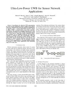
Wireless sensing and radio frequency identification (RFID) are the key technological enabler to realize the vision of the internet of things. Tiny RFID tags with sensors will be embedded into our daily objects or even be implanted into human bodies, monitoring their status and surrounding environment. Compared with traditional RFID, implementing such sensor tags is still challenging. First, the sensor interface that used to quantize the analog sensing information complicates the tag and increases the power consumption. Moreover, the quantized data from the sensor dramatically increase the burden of data transmission. The passive backscattering RFID features low cost transmission but can only achieve a few hundreds of kb/s, which limits the sampling rate or (and) the resolution (the required transmitting rate Rdata = fs ⋅ B , where fs is the sampling rate and B is the resolution of ADC). In [1], a 12 μW back-scattering based body sensor tag has been
978-1-4799-3432-4/14/$31.00 ©2014 IEEE
Figure 2. The operation of PPM-UWB modulator
demonstrated as shown in Fig. 1(a). However, it tends to target data rates between 100 and 200 kb/s, which is limited in applications required high resolution or sampling rate. On the other hand, active transmitting (Fig. 1(b)) provides sufficient speed, yet is too power-hungry to be powered by RF energy as traditional passive RFID tag [2]. Some strategies employ single slope ADC consisting of triangular wave generator (TWG) and time digital converter (Fig.1 (c)) because of its simplicity, while the data rate of transmission is still proportional to the product of sampling rate and resolution of ADC [3]. In [4], a clockless system converts the sensed data into PWM signal and transmits the PWM signal by FSK carrier as shown in Fig. 1(d). Hence, the TDC and digital part is moved to the receiver side which leads to power saving of
2503
sensor tag. Nevertheless the LC-VCO for FSK modulation is complex and power hungry. In this work, a novel sensor tag has been designed using PPM modulator and IR-UWB transmitter in order to reduce the transmitter power as shown in Fig. 2. The tag is powered by RF wave from reader and transmits impulse UWB signal back to the reader which enables high accurate TOA estimation. In order to reduce the number of bits transmitted, a Pulse Position Modulator is employed to convert the analog signal to baseband signal with various pulse position, which is directly transmitted by the IR-UWB transmitter. To demonstrate the advantage of the proposed technique, a power and resolution model is set up for analysis. And a sensor tag is designed in 180 nm CMOS process to verify the practicality. The remainder of this paper is organized as follows. The proposed PPM-UWB approach is discussed in Section II. This is followed by circuit description and simulation results in Section III. The conclusions are presented in Section IV. II.
Figure 3. Transmission power of conventional approach and proposed PPM-UWB approach
SYSTEM DESCRIPTION
A. PPM-UWB Modulator Innovation The impulse UWB radio provides a high-speed wireless link with a low-power and low-complexity transmitter implementation. Moreover the short duration of pulses enables accurate Time-of-Arrival (TOA) estimation [5]. Taking the advantage of UWB’s low-complexity and high-resolution TOA estimation, we introduce a time-domain ADC based on pulse position modulated (PPM) modulation and UWB radio. Fig. 2 shows the block diagram of PPM-UWB modulator. By comparing the analog signal with a tunable triangular waveform, the sensor information is represented by a baseband signal with variable pulse position. Therefore the PPM sample rate and sampling rate are equal. Thanks to the time-domain nature of IR-UWB, each PPM signal can be directly converted to a very short pulse by an extremely simple UWB transmitter. On the reader side, the intervals of received pulses are measured by TOA estimation, which corresponds to a time-to-digital conversion of the original analog samples. Therefore the time-domain ADC is similar to a single-slope ADC that is made wireless, but moving the complex and power-hungry TDC to the reader side. This timebased method leverages variable pulse to present sampled data at a rate proportional to the sampling rate rather than the product of sampling rate and resolution. Therefore, this would enable far fewer transmit cycles than traditional solution when capturing signals with relatively high resolution. Moreover, the IR-UWB technique provides superior power efficiency compared to other state-of-art radio transmitters like FSK in [6] due to the very low duty cycle characteristic, which helps to further degrade the transmitting power. In addition, the rising/falling slopes and dynamic range of triangular wave generator can be tunable by commands from reader, allows the sensor tag to detect different signals with various bandwidth and amplitude. B. PPM-UWB Modulator Operation Fig. 2 demonstrates the operation of the PPM-UWB modulator. To measure PPM sample duration, a short pulse should be generated at both rising edge of triangular wave
Figure 4. System resolution versus TOA estimation error
(TW) signal and falling edge of the PPM signal generally as shown in Fig. 2. In this work, to further reduce the power consumption, we have taken a step further. It should be noted the delay between two rising edges of TW signals are fixed, which is determined by the TW period. Since the triangular wave generator (TWG) in sensor tag is configured by the reader, it is easy for reader to achieve the TW signal period upon current settings if the TWG period information under different conditions is stored in advance. Then the reader is able to estimate the TOA of following triangular wave’s rising edge with the TOA of the first one. Only one pulse which is called synchronization pulse will be generated at rising edge of the triangular wave signal in the beginning of operation for reader-tag synchronization and then the IR-UWB transmitter only triggers at the falling edge of the PPM signal. The other pulses at rising edge of the triangular wave signal can be eliminated (see the red ones). The PPM duration can be easily measured by eliminating the TOA of rising edge of the triangular wave signal from the TOA of falling edges of PPM signal. Therefore the sampling rate, PPM signal rate and pulse rate are nearly equal. C. Power and Resolution Model Wireless transmission power consumption dominates the power consumption for typical circuits in bio-sensor applications [7]. And the transmission power is determined by the number of bits transmitted. Therefore the transmission data rate and estimate power which uses general energy per bit of radio can be employed to represent the energy cost of the entire system. In a sensor tag approach based on conventional ADC, the data rate of transmitter is Rdata = fs ⋅ B (1) where fs is the sampling frequency of interface and B is the resolution of ADC. The resulting power of the transition block is then
2504
PTX =fs ⋅ B ⋅ Eb
(2)
where Eb is energy per bit of the transmitter. In subsequent analysis, the Eb of typical radio used to show tradeoffs is 3 nJ/bit, which is consistent with the general performance of modern radio transmitter [6]. While the energy per pulse of UWB transmitter is 27 pJ/pulse in this tag. In the proposed PPM-UWB approach, only one transmission cycle is needed per sample, which is independent of the interface resolution. The resulting power of the transmission block is then PTX =fs ⋅ Eb
(3)
Fig. 3 shows the power of transmitter versus sampling rate from 1 kS/s to 10 MS/s (sample per second) for proposed PPM-UWB approach and conventional approach based on ADCs and typical radio. The resolution of PPM-UWB tag depends on the TOA estimation error on the reader side. The upper and lower limits of triangular wave should be tunable based on the swing range of incoming signals to maximize the system resolution [4]. If other non-ideal factors are ignored, and the triangular wave range is slightly larger than dynamic range of input signal, the resolution can be calculated by resolution =log 2 [
Tr 1 1 ] ⋅ ⋅ Ts fs TOA _ error
(4)
Tr is the ratio of rising state to the total period of TW, Ts TOA_error is the TOA estimation error on the reader side. Fig. 4 shows system resolution versus TOA estimation error T from 1ns to 10ns for proposed PPM-UWB tag where r is Ts selected to be 2/3.
where
To verify the performance improvement of proposed tag, the models developed above are used to map the power cost. In our analysis, the goal is to develop an 8bits, 1MS/s sensor tag. For the typical tag shown in Fig. 1(b), when the ADC resolution is 8bit, a 1 MS/s sampling rate will result in 24 mW transmission power consumption. However, for the PPMUWB tag, 1 MS/s sampling rate corresponds to 27 μW transmission power consumption regardless of the resolution. Therefore this unique architecture is expected to reduce transmission power consumption by nearly 3 orders of magnitude over tags based on ADCs and typical radio. To meet 8 bit resolution requirement with 1 MS/s sampling rate in PPM-UWB tag, the TOA estimation error need to be less than 2.6 ns as shown in Fig. 4. When the TOA estimation error increases to 5 ns, the resolution decreases to 7 bit. However, for a fixed TOA estimation error, when the sampling rate decreases, the system resolution increases, which allows a tradeoff between sampling rate and resolution. III.
CIRCUIT DESCRIPTION AND SIMULATION
Fig. 5 illustrates the proposed block diagram of sensor tag. The system consists of four main blocks: power scavenging unit, UHF/UWB transceiver, sensor interface and control logic.
Figure 5. Block diagram of proposed sensor tag
The power scavenging unit provides the power supply for the system from RF wave. A demodulator is employed to recover the data symbols from RF wave. A PPM-based analog-to-time converter is employed as sensor interface to quantize the output of the sensor. An IR-UWB transmitter, in the 3.1-10.6GHz band, is utilized to wirelessly transmit PPM signal from the PPM modulator. The control logic decodes these symbols to identify and execute the commands from the reader and trigger the tag’s finite-state machine. The power scavenging unit includes a rectifier, two LDOs and other components as shown in Fig. 6. The rectifier consisting of a chain of CMOS half-wave multipliers rectifies the incoming RF wave to a dc voltage in storage capacitor. Two LDOs are used for generating regulated voltage for circuits. LDO1 provides a 1.8V supply to comparator of PPM modulator which reduces delay variation and to the IR-UWB transmitter which improves the pulse amplitude. LDO2 generates a 1.2V supply for TWG to reduce power consumption. TWG is a key block in the PPM-UWB system. The proposed circuit employs a very simple approach that a pair of complementary current source and sink linearly charge and discharge the sampling capacitor to generate TW in [4]. Compared to [4], the power hungry feedback OTAs and bias circuits VSOURCE and VSINK, are eliminated in this design. Therefore the power consumption is reduced significantly. However the nonlinearity of the PPM transfer function will limit the resolution of ADC. This can be solved by introducing digital calibration on the reader where power constraints are far more relaxed. The rising/falling slopes of TWG could be changed by a set of binary scaled current mirrors that are digitally controlled by DP0~3 and DN0~3. The upper and lower limits of the swing range, Vhigh and Vlow, can be set to VDD-0.1 V and VSS+0.1 V to provide a wide range close to supply rails, or slightly above the range of signals at the output of the analog front-end to improve the system resolution [4]. The adjustable TWG allows the user to trade off the system’s bandwidth, sampling rate, swing range and resolution based on the input signals and the number of channels. To realize wide operating range, the comparator employs a rail to rail input stage. The propagation delay variation with respect to the input common mode should be less than one LSB of the time measurement to avoid ADC distortion. This is done by utilizing extra differential pairs operating in the mid-voltage region, such that the slew rate is dominated by the bias current. In this way, a constant slew rate is achieved. Furthermore a sample and hold circuit is used to sample the analog input and ensure stable data during comparison. A continuous-time filter architecture and OOK modulation is employed in IR-UWB TX which is driven by the PPM signal from the PPM modulator.
2505
CONCLUSION
IV.
This paper proposed a sensor tag with a time-domain ADC in 180 nm process. RF wave powers up the tag. PPM Modulator and IR-UWB transmitter are employed to convert and transmit the analog sensing information. Simulation results show the proposed approach reduces power consumption by nearly 3 orders of magnitude over traditional solutions and consumes 85 μW for 1.5 MS/s sampling rate. TABLE I.
Figure 6. Schematic of main building blocks
PERFORMANCE COMPARISON [2]
[8]
This Work
Technology
130nm
130nm
180nm
Frequency Band
MICS
MICS/ISM
UWB/UHF
TX Date Rate
100kb/s
200kb/s
1.5MS/s
Total Power
500µW
397µW
85µW
Note on Total Power
AFE, 8b ADC, TX (100% on)
AFE, 8b ADC, Digital blocks, TX (100% on)
PPM-UWB Modulator, other blocks in Fig. 5, TX (100% on)
FOM (10-9)
5
1.985
0.007
Figure 7. Chip layout
ACKNOWLEDGMENT Dongxuan Bao thanks financial support from China Scholarship Council for study at KTH-Royal Institute of Technology. This work was supported in part by Vinnova (The Swedish Governmental Agency for Innovation Systems) through the Vinn Excellence centers program. REFERENCES Figure 8. Simulation results of PPM-UWB system
[1]
The proposed PPM-UWB system has been designed in 1P6M 0.18-μm CMOS process, shown in Fig. 7. Simulation results show that the TWG block had full scale ISource and ISink equal to 10 μA and 21 μA, respectively. With maximum TW swing range (from 0.1V to 1.1V at 1.2V supply), the sampling frequency could be adjusted in 225 steps from 100 kHz to 1.5 MHz. The sensitivity of power scavenging unit is 14dBm. The simulation results of PPM-UWB modulator is shown in Fig. 8. The power consumption of sensor tag is simulated to be 85 μW at 1.5 MHz pulse rate while the PPMUWB modulator consumes 70 μW. As each sample corresponds to a PPM signal or a UWB pulse, the sampling rate is 1.5 MS/s. The comparison with previous sensing prototypes are summarized in TABLE-I. Note that Power (5) Rdata where Power is the total chip power, R data is the transmitter data rate. The resolution of this work is assumed to be 8 bit. Then the data rate is 12Mb/s at 1.5MS/s sampling rate. FOM =
[2]
[3]
[4]
[5]
[6]
[7]
[8]
2506
J. Yoo, et al., “A 5.2 mW Self-Configured Wearable Body Sensor Network Controller and a 12 μW Wirelessly Powered Sensor for a Continuous Health Monitoring System,” ISSCC Dig. Tech. Papers, pp. 290-291, Feb. 2009. S. Rai, et al., “A 500μW neural tag with 2μVrms AFE and frequencymultiplying MICS/ISM FSK transmitter,” ISSCC Dig. Tech. Papers, pp. 212-213, Feb. 2009. Dong Li, et al., “Wireless Sensing System-on-Chip for Near-Field Monitoring of Analog and Switch Quantities,” IEEE Tran. Industrial Electronics, vol. 59, no. 2, pp. 1288-1299, Feb. 2010. M. Yin and M. Ghovanloo, “A clockless ultra low-noise low-power wireless implantable neural recording system,” IEEE International Symp. Circuits and Systems, pp. 1756-1759, May 2008. Zhuo Zou, et al., “A Low-Power and Flexible Energy Detection IRUWB Receiver for RFID and Wireless Sensor Networks,” IEEE Tran. Circuits ans System I, vol. 58, no. 7, pp. 1470-1482, Jul. 2011. J. L. Bohorquez, J. L. Dawson, and A. P. Chandrakasan, “A 350 μW CMOS MSK transmitter and 400 μW OOK super-regenerative receiver for medical implant communications,” in 2008 Symp. VLSI Circuits Dig. Tech. Papers, 2008, pp. 32–33. F. Chen, et al., “Design and Analysis of a Hardware-Efficient Compressed Sensing Architecture for Data Compression in Wireless Sensors,” IEEE J. Solid-State Circuits, vol. 47, no. 3, pp. 744-756, Mar. 2012. F. Zhang, et al., “A Batteryless 19μW MICS/ISM-Band Energy Harvesting Body Area Sensor Node SoC,” ISSCC Dig. Tech. Papers, pp. 298-300, Feb. 2012.