Home
Search
Collections
Journals
About
Contact us
My IOPscience
An investigation of PDMS structures for optimized ferroelectret performance
This content has been downloaded from IOPscience. Please scroll down to see the full text. 2014 J. Phys.: Conf. Ser. 557 012104 (http://iopscience.iop.org/1742-6596/557/1/012104) View the table of contents for this issue, or go to the journal homepage for more
Download details: IP Address: 152.78.66.123 This content was downloaded on 23/12/2015 at 15:10
Please note that terms and conditions apply.
PowerMEMS 2014 Journal of Physics: Conference Series 557 (2014) 012104
IOP Publishing doi:10.1088/1742-6596/557/1/012104
An investigation of PDMS structures for optimized ferroelectret performance J Shi, D Zhu and S P Beeby Electronics and Electrical Engineering Group, Electronics and Computer Science University of Southampton, Southampton, SO17 1BJ, UK E-mail:
[email protected] Abstract: This paper reports the ANSYS simulation and fabrication processes for optimising PDMS ferroelectret performance. The proposed model extends the previously published analytical models and compares this with simulation of individual void geometry. The ferroelectret material is fabricated from PDMS using 3D-printed plastic moulds. The analytical model and Ansys simulation results predict the variation in performance of the PDMS ferroelectret with the different void geometry and surface charge density. The theoretical maximum piezoelectric coefficient d33 achieved was about 220 pC/N. The experimental maximum d33 obtained was 172 pC/N.
1. Introduction A ferroelectret is a type of polymer electret that displays piezoelectric like properties, which is a polymer film with cellular structure. The thickness of ferroelectret films typically ranges from a few dozen to a hundred microns. The geometry of internal voids typically a lens shape with a thickness and width from a few to dozen micrometers. The separated positive and negative charges which are trapped on the upper and lower gas-polymer interfaces in the voids cause the piezoelectric like property of ferroelectrets, because the separated charged form macroscopic dipoles in the voids. The macroscopic dipole moment can be determined by the quantity of the charges and the distance between the separated charges. When the ferroelectret is compressed by an external mechanical load, its volume decreases and compensating charges are generated on the external surface. The resulting macroscopic behaviour of ferroelectret is very similar with the well-known piezoelectric materials; but its microscopic mechanism of charge generation is entirely different from the latter. For ferroelectret, the interior voids not only reduce the overall mass and stiffness, but also generate great dipoles when the separated positive and negative charges are trapped on the upper and lower surface of the voids. Due to the combined effects of the internal dipole moment and the anisotropic cellular polymer structure, the majority of volume change takes place in the voids. Therefore when loaded the distance between positive and negative charges decreases, the dipole moment decreases. The amount of compensating charge decreases and a flow of charge is generated, which presents a strong piezoelectric like effect for ferroelectret [1]. Hence, ferroelectrets are utilized as functional materials in electromechanical sensors and actuators, also as electrically charged layers in electrostatic transducers [2, 3]. The piezoelectric like properties of ferroelectrets has already been theoretically analysed [4-7]. However, most ferroelectrets are formed by a modified film blow and extrusion process for producing the desired cellular structures. The results of this fabrication method are usually ill-controlled in both individual void geometry and overall cellular structure, and the existing modelling methods to approximate the piezoelectric like properties of these materials and structures are simplified models that do not consider individual void geometry and void distribution. Therefore, in this paper we report Content from this work may be used under the terms of the Creative Commons Attribution 3.0 licence. Any further distribution of this work must maintain attribution to the author(s) and the title of the work, journal citation and DOI. Published under licence by IOP Publishing Ltd 1
PowerMEMS 2014 Journal of Physics: Conference Series 557 (2014) 012104
IOP Publishing doi:10.1088/1742-6596/557/1/012104
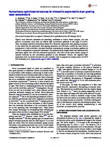
a design, fabrication and testing methodology for optimising PDMS ferroelctret performance based on polymer MEMS fabrication technology. 2. Model Piezoelectricity of ferroelectrets has been theoretically analyzed with a simplified model based on charged parallel polymeric and gaseous layers, which includes the finite-element calculations [4-7]. The ANSYS simulation work of this research modelled a cellular PDMS structures (Figure 1) containing a layer of rectangular voids. The ANSYS results predicted deformation of the voids when the structure is subject to an external mechanical load. Assuming the charge densities of the voids surface was uniform, the variation of the charge on the external surface can be calculated by the average of the deformations. Then the piezoelectric coefficient d33 can be estimated as: 𝑑33 = 2𝜀1 𝜎(𝑥2 ∆𝑥1 + 𝑥1 ∆𝑥2 )(2𝑥1 + 𝜀1 𝑥2 )−2 𝐹 −1 (1) Where 𝜀1 is the dielectric constant of air and the relative dielectric constant of PDMS; 𝜎 is the charge density on void surface; 𝑥1 and 𝑥2 are the thickness of solid and void layers, respectively; ∆𝑥1 and ∆𝑥2 are the variations of the thickness and F is the external force. For analytical model, the piezoelectric coefficient d33 can be directly obtained from: (2) 𝑑33 = 2𝜀1 𝜎𝑡𝑟1 (1 − 𝑠𝑟1 )2 𝑠𝑟1 −1 [2 + 𝜀1 𝑡𝑟1 ]−2 𝑐33 −1 Where 𝑠𝑟1 is the ratio of the effective area of the void layers to the effective area of the solid layers; 𝑡𝑟1 is the ratio of the thickness of void layers to the thickness of solid layers; 𝜎 is the charge density on void surface; 𝜀1 is the dielectric constant of air and the relative dielectric constant of PDMS; 𝑐33 is the elastic modulus of PDMS.
Figure 1. Cellular structures with a layer of rectangular voids
Figure 2. The image of a prepared 3D-printed mould
3. Fabrication and Measurement 3.1. 3D-printed mould preparation A 3D CAD model of the mould structure was constructed with Solidworks 2012 (Dassault Systems, MA, USA), exported as an STL-format file, and printed on a Connex350TM 3D printing system (Stratasys, MN, USA). The used moulds can be made from VeroWhitePlusTM, VeroGeryTM or VeroClearTM, generated in ‘glossy’ printer mode on a bed of FullCure®705 support material. Because the 3DP material inhibits PDMS polymerization and the printed structure tends to warp some extent when it is removed from the printer, the resulting 3D-printed structure is not directly suitable as a mould for PDMS casting. The moulds should be baked in oven at 80 °C overnight. In this bake step, the moulds were placed and glued to a glass slide by a drop of degassed non-polymerized PDMS, with its base in contact with the PDMS film. After this procedure, the glass-backed moulds were exposed to a silane vapour for 1 hour to coat it with a thin layer of trichloro(1H,1H,2H,2H2
PowerMEMS 2014 Journal of Physics: Conference Series 557 (2014) 012104
IOP Publishing doi:10.1088/1742-6596/557/1/012104
perfluorooctyl)silane (Sigma Aldrich, MO, USA). An example of a finished mould of VeroClearTM material, with outer dimensions of 38 × 38 mm, is shown in Figure 2. Depending on the maximum precision of the 3D printer and the restrictions of fabrication process, the thickness of the solid layer and void layer was selected as 2 mm and 1.6 mm, respectively; the width of the voids and the gap between the voids was selected as 0.75 mm and 0.5 mm, respectively. 3.2. PDMS casting and Bonding Liquid PDMS and curing agent (Sylgard 184 from Dow Corning, MI, USA) were mixed at a 10:1 weight ratio and the mixture was degassed in a vacuum desiccator. The degassed PDMS was poured into the glass-backed moulds which were again degassed and then baked at 80 °C for 1 hour. After detaching the polymerized PDMS from the moulds, an oxygen plasma treatment was applied on the patterned surface of PDMS layers (Femto Asher, Diener, Germany, 30 S at 35-40W) and then bonded to the other PDMS layers. To optimise the bonding effect, the samples were assembled with bonding times of 30 s, 60 s, 90 s and 120 s, separately. The bonded PDMS was then baked in oven at 80 °C for 1 hour to improve the bonding effect, and also recover the original hydrophobic PDMS surface chemistry. The schematic of PDMS casting and bonding processes, and the cross-section view of the bonded sample are illustrated in Figure 3 and Figure 4, separately.
PDMS Part 1 Voids
PDMS Part 2
0.5mm
Figure 4. Image of cross-section view of single layer ferrelectret foam
Figure 3. Schematic of fabrication processes
3.3. Corona charging and Measurement The samples were polarized with a point-to-plane corona discharge in air under ambient conditions. A corona-tip voltage of -25 kV and a charging time of 30 s were employed. Its piezoelectric charge constant d33 was measured using a PiezoMeter (PM300, Piezotest Ltd). 4. Results and Discussion An analytical result is provided in Figure 5, which numerically illustrates the impact of the different void geometry. While the ratio of the effective areas of the solid and void layers is increased, the piezoelectricity of PDMS ferrelectret was reduced. In other word, the piezoelectric properties of the PDMS ferreoelectret improved with increasing void area. In contrast, when the ratio of the thickness of the solid and void layers is increased, the piezoelectric properties of the PDMS ferroelectret was improved and the optimised point has been demonstrated at around 0.8, with a peak piezoelectricity of 220 pC/N. However, considering the feasibility of the fabrication processes, the optimized structure which can be achieved with sr1=0.4 and tr1=0.8. Based on these ratios, the geometry of void structure is designed as 0.75 mm in width and 1.6 mm in height, and the distance between the voids and the thickness of the whole film is selected as 0.5 mm and 5.6 mm, respectively. For this structure, the theoretical d33 values is 62.5 pC/N at surface charge density = 100 μC/m2.
3
PowerMEMS 2014 Journal of Physics: Conference Series 557 (2014) 012104
IOP Publishing doi:10.1088/1742-6596/557/1/012104 250
pC/N
200 150
86.5
100 50
62.5
0 0
100
200
Surface Charge Density Ansys simulation results
Figure 5. Analytical rectangle model results varying with the size of voids
300
(μC/m2)
Analytical model results
Figure 6. Analytical model results and Ansys simulation d33 results for rectangle voids
Figure 6 shows a comparison of ANSYS simulation results and analytical model results to illustrate the influence of the surface charge density based on the designed geometry. There was an obvious deviation between the ANSYS simulation results and analytical model results because the analytical model was based on the principle of a rigid body. In other word, the bending effects that happened on the upper and lower gas-polymer interfaces of the voids was also not considered. The realized geometry of the void inside the PDMS ferroelectret is illustrated in Figure 7. The realized geometry of void is different to the model due to the precision of fabrication process. The d33 value of the PDMS ferroelectret was experimentally measured to be around 70 pC/N. The performance of the PDMS ferroelectret can be influenced by plasma treatment. The impact of plasma treatment time is illustrated at Figure 8. The performance of the PDMS ferroelectret was substantially grown during the plasma treatment duration increasing. The experimental maximum d33 obtained is about 170 pC/N at 120 s plasma treatment condition. The possible reason of this phenomenon is the surface charge density of PDMS can be significantly improved by increase in plasma treatment time. 180 160
d33 (pC/N)
140 120 100 80
60 40 0
30
60
90
120
150
plasma treament Time (S)
Figure 7. The image of cross section view of Realized voids
Figure 8. The piezoelectric performance varying with duration of plasma treatment
4
PowerMEMS 2014 Journal of Physics: Conference Series 557 (2014) 012104
IOP Publishing doi:10.1088/1742-6596/557/1/012104
5. Conclusion and future work In this work, the simulation and testing of PDMS ferroelectret with a variety of void geometries and surface charge density has been investigated. The piezoelectric properties of PDMS ferroelectret are improved with an enhancement of the void area and the optimized structure was achieved with the ratio 𝑡𝑟1 =0.8 for a single void layer of PDMS ferroelectret material. In addition, the performance of PDMS ferroelectret can be significantly affected by the plasma treatment. In the future, PDMS ferroelectret will be optimised for different shapes, multilayer void structure and scaling down based on a MEMS fabricated mould. 6. Acknowledgement This work was performed under the SPHERE IRC funded by the UK Engineering and Physical Sciences Research Council (EPSRC), Grant EP/K031910/1. 7. References [1] M. Paajanen, “The cellular polypropylene electret material-Electromechanical properties”, Dissertation, VTT Publications 436, Technical Research Centre of Finland, Tampere University of Technology, 2001. [2] J. Backman. “Audio applications of electrothermomechanical film (ETMF)”, J. Aud. Eng. Soc., vol. 38 (5), pp. 364-371, 1990. [3] M. Paajanen, J. Lekkala, and K. Kirjavainen, “Electromechanical film (EMFi) - a new multipurpose electret material”, Sens. Actu. A: Phys., vol. 84 (1-2), pp. 95-102, 2000. [4] J. Hillenbrand and G. M. Sessler, “Piezoelectricity in cellular electret films”, IEEE Trans. Dielect. Electr. Insul., vol. 7 (4), pp. 537-542, 2000. [5] M. Paajanen, J. Lekkala, and H. Välimäki, “Electromechanical modeling and properties of the electret film EMFi”, IEEE Trans. Dielect. Electr. Insul., vol. 8 (4), pp. 629-636, 2001. [6] M. Paajanen, H. Välimäki, and J. Lekkala, “Modelling the sensor and actuator operations of the ElectroMechanical Film EMFi”, Proceedings, 10th International Symposium on Electrets, 2224 September 1999, Delphi, Greece (IEEE Service Centre, Piscataway, NJ, USA 1999), pp. 735-738. [7] G. M. Sessler and J. Hillenbrand, “Electromechanical response equations of cellular electret films”, Proceedings, 10th International Symposium on Electrets, 22-24 September 1999, Delphi, Greece (IEEE Service Centre, Piscataway, NJ, USA 1999), pp. 261-264.
5