DL-TR-2006-010
An overview of FPGAs and FPGA programming; Initial experiences at Daresbury Richard Wain, Ian Bush, Martyn Guest, Miles Deegan, Igor Kozin and Christine Kitchen November 2006 Version 2.0
Council for the Central Laboratory of the Research Councils
© 2006 Council for the Central Laboratory of the Research Councils Enquiries about copyright, reproduction and requests for additional copies of this report should be addressed to: Library and Information Services CCLRC Daresbury Laboratory Daresbury Warrington Cheshire WA4 4AD UK Tel: +44 (0)1925 603397 Fax: +44 (0)1925 603779 Email:
[email protected]
ISSN 1362-0207
Neither the Council nor the Laboratory accept any responsibility for loss or damage arising from the use of information contained in any of their reports or in any communication about their tests or investigations.
An overview of FPGAs and FPGA programming; Initial experiences at Daresbury November 2006 Version 2.0 Richard Wain, Ian Bush, Martyn Guest, Miles Deegan, Igor Kozin and Christine Kitchen Computational Science and Engineering Department, CCLRC Daresbury Laboratory, Daresbury, Warrington, Cheshire, WA4 4AD, UK
Abstract This report will provide a brief introduction to Field Programmable Gate Arrays (FPGAs), the key reasons for their emergence into the High Performance Computing (HPC) market and the difficulties of assessing their performance against that of conventional microprocessors. It will also discuss FPGA programming tools and the key challenges involved in programming these devices. As well as providing some background information on FPGAs and FPGA programming this report will cover our initial experiences of FPGA programming with specific reference to the Cray XD1 system.
Contents 1
Introduction.....................................................................................................................................2 1.1 FPGAs and HPC....................................................................................................................2 1.2 FPGA Performance ...............................................................................................................3 2 Programming an FPGA...................................................................................................................4 2.1 Hardware vs. Software Design Flow.....................................................................................5 2.2 Hardware vs. HPC Software Practice....................................................................................6 3 Programming Languages and Tools................................................................................................7 3.1 VHDL & Verilog...................................................................................................................7 3.1.1 Xilinx tools ..................................................................................................................8 3.1.2 FPGA Advantage Mentor graphics tools .....................................................................8 3.2 Pseudo-C High level languages.............................................................................................8 3.2.1 Mitrion-C and Mitrion-IDE .........................................................................................9 3.2.2 Handel-C and Celoxica DK Design Suite ..................................................................10 3.2.3 Nallatech DIME-C and DIMETalk............................................................................11 3.3 Other languages and tools ...................................................................................................12 4 Initial experiences of FPGA programming at Daresbury..............................................................12 4.1 Development board VHDL .................................................................................................13 4.2 Development board Handel-C .............................................................................................13 4.3 Cray XD1 VHDL ................................................................................................................14 4.4 Cray XD1 Handel-C ............................................................................................................16 4.5 DIME-C...............................................................................................................................17 4.6 Conclusions .........................................................................................................................18
FPGA Overview
1
November 2006
1 1.1
Introduction FPGAs and HPC
A Field-Programmable Gate Array or FPGA is a silicon chip containing an array of configurable logic blocks (CLBs). Unlike an Application Specific Integrated Circuit (ASIC) which can perform a single specific function for the lifetime of the chip an FPGA can be reprogrammed to perform a different function in a matter of microseconds. Before it is programmed an FPGA knows nothing about how to communicate with the devices surrounding it. This is both a blessing and a curse as it allows a great deal of flexibility in using the FPGA while greatly increasing the complexity of programming it. The ability to reprogram FPGAs has led them to be widely used by hardware designers for prototyping circuits. Over the last two to three years FPGAs have begun to contain enough resources (logic cells/IO) to make them of interest to the HPC community. Recently HPC hardware vendors have begun to offer solutions that incorporate FPGAs into HPC systems where they can act as co-processors, so accelerating key kernels within an application. Cray were one of the first companies to produce such a system with the XD1, a system originally designed by OctigaBay [1]. SGI quickly emerged as the main competitor to Cray producing the RASC Module (v1) and later the RASC RC100 Blade each of which could be integrated with SGI Altix servers [2]. SRC computers produces a range of reconfigurable systems based on it’s IMPLICIT + EXPLICIT architecture and MAP processor [3]. There are a number of other companies producing reconfigurable hardware for HPC, one of the most recent to enter the market being DRC computers who produce FPGA modules that can be plugged directly into an HTX slot on an AMD Opteron processor [4]. DRC have been working with Cray to implement this technology in the follow up to the XT3 [5]. Another interesting piece of hardware that has recently been announced by Nallatech is the H100 series of FPGA based expansion blades for the IBM BladeCenter [6]. All of the systems mentioned above are based on FPGAs supplied by a single company, Xilinx. Xilinx are the largest global producer of programmable logic devices [7] and the Xilinx Virtex series has been adopted as the FPGA of choice for HPC. The reality of double precision floating-point capable FPGAs really arrived in 2002 with the Virtex II Pro FPGA, which contains up to one hundred thousand logic cells as well as dedicated DSP slices containing 18-bit by 18-bit, two’s complement multipliers. These chips can be clocked at up to 400MHz [8]. The Virtex 4, released in 2004, has built considerably on the Virtex II Pro with up to two hundred thousand logic cells, more DSP slices and more 18-bit by 18bit multipliers, and now clocking up to 500 MHz [9]. Unfortunately, the 18-bit by 18-bit multipliers in the Virtex II Pro and Virtex 4 FPGAs are not well suited to the requirements of floating point IP cores. Xilinx have attempted to redress this problem by providing a larger number of 25-bit by 18-bit multipliers on their new Virtex 5 range of FPGAs [10]. The Virtex 5 is the first FPGA on a 65nm process and once again provides increased clock speeds, higher logic density and a number of other optimizations over previous generations. One of the distinct advantages of FPGAs over conventional microprocessors is that they still benefit from a clock-speed increase with each new generation of hardware. As an FPGA consists of an array of CLBs the array can simply be expanded as the process shrinks below 65nm avoiding the requirement for extensive re-engineering of the architecture for each new generation of chip. The recent surge in FPGA interest from the HPC community (Spearheaded by OpenFPGA [11]) has come at a time when conventional microprocessors are struggling to keep up with Moore’s law. This slowing of performance gains in microprocessors along with the increasing cost of servicing their considerable power requirements has led to an increased interest in any technology that might offer a cost-effective alternative. The use of FPGAs in HPC systems can provide three distinct advantages over conventional compute clusters. Firstly, FPGAs consume less power than conventional microprocessors; secondly, using FPGAs as accelerators can significantly increase compute density; and thirdly, FPGAs can provide a significant increase in performance for a certain set of applications.
FPGA Overview
2
November 2006
1.2
FPGA Performance
While the headline performance increase offered by FPGAs is often very large (>100 times for some algorithms) it is important to consider a number of factors when assessing their usefulness for accelerating a particular application. Firstly, is it practical to implement the whole application on an FPGA? The answer to this is likely to be no, particularly for floating-point intensive applications which tend to swallow up a large amount of logic. If it is either impractical or impossible to implement the whole application on an FPGA, the next best option is to implement those kernels within the application that are responsible for the majority of the run-time, which may be determined by profiling. Next, the real speedup of the whole application must be estimated once the kernel has been implemented in a FPGA. Even if that kernel was originally responsible for 90% of the runtime the total speed-up that you can achieve for your application cannot exceed 10 times (even if you achieve a 1000 times speed up for the kernel), an example of Amdahl’s law [12], that long time irritant of the HPC software engineer. Once such an estimate has been made, one must decide if the potential gain is worthwhile given the complexity of instantiating the algorithm on an FPGA. Then, and only then, one should consider whether the kernel in question is suited to implementation on an FPGA. In general terms FPGAs are best at tasks that use short word length integer or fixed point data, and exhibit a high degree of parallelism [13], but they are not so good at high precision floating-point arithmetic (although they can still outperform conventional processors in many cases). The implications of shipping data to the FPGA from the CPU and vice versa [14] must also come under consideration, for if that outweighs any improvement in the kernel then implementing the algorithm in an FPGA may be an exercise in futility. FPGAs are best suited to integer arithmetic. Unfortunately, the vast majority of scientific codes rely heavily on 64 bit IEEE floating point arithmetic [15] (often referred to as double precision floating point arithmetic). It is not unreasonable to suggest that in order to get the most out of FPGAs computational scientists must perform a thorough numerical analysis of their code, and ideally reimplement it using fixed point arithmetic or lower precision floating-point arithmetic. Scientists who have been used to continual performance increases provided by each new generation of processor are not easily convinced that the large amount of effort required for such an exercise will be sufficiently rewarded. That said the recent development of efficient floating point cores [16] has gone some way towards encouraging scientists to use FPGAs. If the performance of such cores can be demonstrated by accelerating a number of real-world applications then the wider acceptance of FPGAs will move a step closer. At present there is very little performance data available for 64-bit floating-point intensive algorithms on FPGAs. To give an indication of expected performance we have therefore used data taken from the Xilinx floating-point cores (v3) datasheet [16]. Table 1 illustrates the theoretical peak performance for basic double precision floating point operations in the largest Xilinx Virtex-5 FPGA1.
Device
Multiply performance Gflop/s
Add performance Gflop/s
Fused Add/Mult performance Gflop/s
Xilinx Virtex-5 LX330
38
111
53
Table 1 Performance of basic floating point operations running on a Xilinx Virtex-5 FPGA [16].
A 3.0GHz Intel Xeon (Woodcrest) dual-core processor has a theoretical peak of 24Gflop/s for double precision floating-point operations2. We can see that a Virtex-5 FPGA could potentially provide between 1.5 and 5 times the performance of the Xeon dual-core processor depending on the ratio of add/subtract to multiply/divide operators in a given FPGA design. This is a crude calculation but it provides some basis for believing that floating point calculations are in no way beyond the realms of 1
To incorporate the maximum number of floating point operators on a single FPGA requires the use of ‘logic only’ cores rather than cores utilising the dedicated DSP slices available on the Virtex-5. 2 This is the performance of both cores combined.
FPGA Overview
3
November 2006
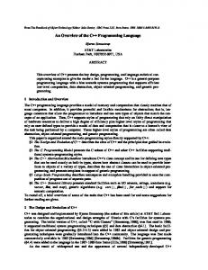
possibility for FPGAs. Recent work has provided further evidence of this [17-23]. In much of this work the performance data that are available are educated guesses based on the results of design synthesis rather than measurements from an implemented design. This data, like that presented in Table 1, is often impressive when compared to current high end microprocessors but still has to be proven on real hardware. As another example Figure 1 provides a summary of DGEMM performance on a range of existing and novel architectures [17, 24, 25]. The results for Virtex II Pro FPGA and the Cell processor are very impressive but again they are also theoretical The aim of our work is in part to generate some meaningful performance values for kernels such as matrix multiplication running on the current generation of FPGAs. It is only when verified performance figures such as these are available that we will be able to make a judgement on the true value of FPGAs to floating-point intensive HPC applications. The proof is, after all, in the pudding!
Figure 1 Performance comparison of DGEMM on a range of architectures [17, 24, 25].
2
Programming an FPGA
Although FPGA technology has been around in some form for many years it is only in the last two to three years that the technology has begun to make any inroads into the HPC market. In the past the vast majority of FPGA users would have been hardware designers with a significant amount of knowledge and experience in circuit design using traditional Hardware Description Languages (HDL) like VHDL or Verilog. These languages and many of the concepts that underpin their use are unfamiliar to the vast majority of software programmers. In order to open up the FPGA market to software programmers, tools vendors are providing an increasing number of somewhat C-like FPGA programming languages and supporting tools. These pseudo-C languages all provide a more familiar development flow that, in many cases, may provide a significant level of abstraction away from the underlying hardware. A number of traditional hardware design languages/tools and pseudo-c languages/tools are covered in greater depth later in this report.
FPGA Overview
4
November 2006
2.1
Hardware vs. Software Design Flow
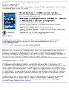
There are several differences between the traditional software design flow and the established Verilog/VHDL design flow for FPGAs. After designing and implementing a hardware design there is a multistage process to go through before the design can be used in an FPGA. The first stage is Synthesis, which takes HDL code and translates it into a netlist. A netlist is a textual description of a circuit diagram or schematic. Next, simulation is used to verify that the design specified in the netlist functions correctly. Once verified, the netlist is converted into a binary format (Translate), the components and connections that it defines are mapped to CLBs (Map), and the design is placed and routed to fit onto the target FPGA (Place and route). A second simulation (post place and route simulation) is performed to help establish how well the design has been placed and routed. Finally, a *.bit file is generated to load the design onto an FPGA. A *.bit file is a configuration file that is used to program all of the resources within the FPGA. Using tools such as Xilinx Chipscope it is then possible to verify and debug the design while it is running on the FPGA. The software design flow has no requirement for a pre-implementation simulation step.
Figure 3 Software design flow
Figure 2 Hardware design flow Compile times for software are much shorter than implementation times for hardware designs so it is practical to recompile code and perform debugging as an iterative process. In hardware it is very important to establish that a design is functionally correct prior to implementation as a broken design
FPGA Overview
5
November 2006
could take a day or more to place and route and could potentially cause damage to system components. Figures 2 and 3 illustrate the differences between software and hardware design flows. 2.2
Hardware vs. HPC Software Practice
Despite the above comments, to the experienced HPC software engineer the design flow of the two paradigms does not seem to be fundamentally dissimilar. Though for hardware there are appreciably more steps, in general this is more often due to having to explicitly perform steps that are nowadays redundant or hidden in the software case. After all it is not so long ago that one of the authors was debugging software on a simulator! This observation in many ways summarizes the differences in design flow between the software and hardware environments. To put it simply, and bluntly, HPC reconfigurable hardware programming is in its infancy, and much of what the software engineer would expect has yet to evolve to the level for which he/she would hope. As a prime example HPC software engineers expect, indeed demand, cross-platform standards. These abstract the scientific problem from the hardware, thus enabling the software engineer to design his or her solution independently of the hardware so enabling the software to be run in many different environments. Nowadays this is the case whether the software is serial or parallel, message passing or multithreaded: For a careful and experienced HPC software engineer code once, run anywhere is now a truly achievable goal. However for hardware this is, as yet, a very far distant goal. As usual the problem is I/O, using the latter term in its most general sense. In fact in all of the languages considered here the real problem is not how to express the scientific algorithm, it is much more how to get data to that algorithm, and how to get the results back. For HPC this is now a very well defined problem. One uses the facilities defined in the ISO standard of your language of choice for disk access, MPI to obtain data from another process, and the = sign to get data from memory. And that sums up the problem; FPGAs a priori know nothing. When you get them they are a blank chunk of semiconductor for you to warp and change to your desire. So they know nothing about memory; they don’t know what kinds of memory are available, what pins the memory is attached to, or anything else you might like to name. And so while you can easily express your problem, the first thing you may have to do is write code to access the outside world. It’s like when you sit down to write Fortran having first to devise your own memory, disk and video controller. FPGAs don’t even know a priori where they are getting a clock from. Of course it is not quite as bad as all that; vendors often provide cores for such low level I/O operations. However these are often specific to a given part, thus hampering portability of even the simplest code and so appreciably increasing the cost of maintenance of the application. Further these are often designed with the hardware engineer in mind, and to a software person the “API” may often appear at best cumbersome, at worst impenetrable. For instance does the software engineer really know enough to handle parity checking the data read from the RAM? All in all, the road from software to hardware programming is long and precipitous, and just learning to “talk the talk” is an achievement in itself. But why should this be so? Well it is partly because FPGAs are not designed with HPC in mind, and in fact their use by HPC is another example of the long tradition of HPC trying to use any hardware that looks “interesting.” FPGAs are more often used in the electronics industry in situations where the cost of development of an ASIC can not be justified. As such once debugged the FPGA is never reprogrammed, and the program will be specific for this electronic device; portability is just not an issue. It is also because the field is very new and standards have not evolved, and as yet are showing no sign of evolving. In fact there is a strong similarity to the early days of the use of parallel computing in HPC. But ultimately one of main problems is, in fact, the power of the FPGA itself. This derives very directly from its great flexibility, and as such programming a given FPGA will strongly depend not only on the FPGA itself, but also on how it is packaged, what components are directly attached to it, and how it is connected to the host CPU, resulting in a plethora of details with which the neophyte must become acquainted before the item of interest, the scientific algorithm, can be implemented
FPGA Overview
6
November 2006
3
Programming Languages and Tools
3.1
VHDL & Verilog
Both VHDL and Verilog are well established hardware description languages. They have the advantage that the user can define high-level algorithms and low-level optimizations (gate-level and switch-level) in the same language. A basic example of VHDL code, the evaluation of the Fibonacci series, is shown below, and it is a good example of the points made above. The code itself is reasonably straightforward for a software programmer to understand, provided that he/she understands that this is a truly parallel language and all lines are executing “at once”. It is also straightforward to simulate a simple design of this nature. However it is surprisingly difficult to implement it in hardware and this difficulty is a direct result of I/O issues. As noted above for a design to work in hardware access is required to resources that are external to the FPGA, such as memory, and an FPGA is, by its very nature, unaware of the components to which it is connected. If you want to retrieve a value from main memory and use it on the FPGA then you need to instantiate a memory controller. While systems such as the Cray XD1 provide cores for communicating with memory, such cores are still complex and unfamiliar to software programmers. Our early experiences with VHDL have indicated that it should only be used for FPGA development if you are in a position to work closely with experienced hardware designers throughout the development process. Fibonacci series example in VHDL [26]: Adapted from http://en.wikipedia.org/w/index.php?title=VHDL&oldid=115145 1 2 3 4 5 6 7 8 9
: : : : : : : : :
entity Fibonacci is port ( Reset : in Clock : in Number : out ); end Fibonacci;
std_logic; std_logic; unsigned(31 downto 0)
In VHDL the 'entity' declaration is like a declaration of a function in C++. In this case, the 'entity' declaration defines a device called Fibonacci. The block of code in parentheses after the word 'port' describes the I/O behaviour of the entity. Lines 4 and 5 define the input ports 'Reset' and 'Clock' and declare them to be of type 'std_logic' (i.e. 1 bit wide). Line 6 defines the output port 'Number' as an unsigned 32 bit value output. Line 8 tells us that we are at the end of the description for the entity called Fibonacci. 10: architecture Fib of Fibonacci is 11: 12: signal Previous : natural; 13: signal Current : natural; 14: signal Next_Fib : natural; 15: 16: begin 17: 18: Adder: 19: Next_Fib