Albrecht Schoy, Amos Ben-Meir, Jeff Trull, Raj Khanna,. Dennis Wendell ... Anderson Vuong, Stanley Yu, Reading Maley, Bruce Kauffmann. AMD, Milpitas, CA.
-
_-
__
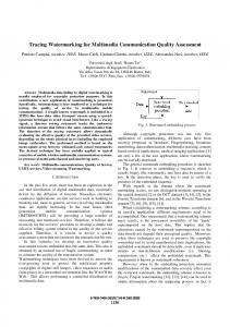
ISSCC97 I SESSION 10 I HIGH-PERFORMANCE MICROPROCESSORS I PAPER FA 10.5 FA 10.5: An X86 Microprocessor with Multimedia Extensions Donald A. Draper, Matthew P. Crowley, John Holst, Greg Favor, Albrecht Schoy, Amos Ben-Meir, Jeff Trull, Raj Khanna, Dennis Wendell, Ravi Krishna, Joe Nolan, Hamid Partovi, Mark Johnson, Tom Lee, Dhiraj Mallick, Gene Frydel, Anderson Vuong, Stanley Yu, Reading Maley, Bruce Kauffmann AMD, Milpitas, CA
This sixth-generation X86 instruction-set compatible microprocessor implements a set of multimedia extensions (MMX). Instruction predecoding to identify instruction boundaries begins during filling of the 32kB two-way set associative L1 instruction Cache after which the predecode bits are stored in the 20kB Predecode Cache as shown in Figure 1. The processor decodes up to two X86 instructions per clock, most of which are decoded by hardware into one to four RISC-like operations, called RISC86 Ops, whereas the uncommon instructions are mapped into ROMresident RISC sequences. The instruction scheduler buffers up to 24 RISC86 operations, using register renaming with a total of 48 registers. Up to six RISC86 instructions are issued out-of -order to seven parallel execution units, speculatively executed and retired in order. The branch algorithm uses two-level branch prediction based on a n 8192-entry branch history table, a 16entry branch target cache and a 16-entry return address stack. The processor incorporates the extensions to the X86 instruction set called the multi-media extensions (MMX). The MMX unit supports instruction and data types that are targeted at increasing performance in communications and multimedia. A single instruction, multiple data (SIMD) technique is used to process multiple operands of 8,16, or 32b in a 64b data path to perform highly-parallel and compute intensive algorithms involved in multimedia applications. The MMXunit supports 57 instructions which allow additions, subtractions, multiplies, multiply-accumulates, shifts (logical or arithmetic) and several other operations, most of which can be executed on any data type. The instruction tag ram contains 512 20b physical tags. The tag ram is logically 2-way set associative, but is physically constructed with 8 sets of tag-tlb comparators and 8 sets of snoop comparators, with 8 tags being read each cycle. This allows all possible synonyms to be checked in a single cycle, a t the expense of layout complexity and area. The tag ram performs a read in the first half cycle and a write in the second half cycle. Write data is available at the beginning of the first half of the cycle and can be bypassed to the read outputs with no read access delay penalty. The sense amp with integrated bypass is shown in Figure 2. The numeric processor PLA contains 17 inputs, 800 minterms, and 104 outputs. The AND and OR planes and their respective sense amps are differential. A partial transistor (drain, no source) provides a matched capacitive environment for dummy bit-lines. The RISC86 Op code ROM contains 4 k x 169bof storage. Bit-lines are single-ended, but are sensed differentially with respect t o a reference line. Four bit-lines share a common reference line, with 4:l column decoding. Minimum pitch metal1 is used for bit-lines with no shielding. This is possible due to the use of resistive load elements for both bit and reference lines. The load elements are constructed of PMOS transistors biased in the linear region. The reference loads have half the resistance of the data loads, and clamp the reference bit-line swing to half that of data bit lines. As the data bit-line voltage swing is limited by the resistive clamp, the signal coupled onto neighboring bit-lines is minimized. This shown in Figure 3, where a lightly loaded bit-line is first coupled
172
1997 IEEE International Solid-State Circuits Conference
down by the adjacent switching bit-lines, and is then pulled back up by the resistive load before sensing occurs. In the caches, in addition to using a 13N-based BIST algorithm, testability is enhanced by a method of array test a t wafer sort (Figure 4). Separate array (vddmx) and wordline (vddwl) vdd supplies are connected in convenient groups to C4 bumps. Independent memory array IDDQ (quiescent current) testing and isolation of memory arrays from logic increases resolution of IDDQ tests. The vddwl and vddmx used in combination with memory tests allow improved data retention testing and detection of cells with marginal read disturb characteristics. The core uses edge-triggered latching (ETL) elements activated by the positive edge of a single-wire clock [l]. Though edgetriggered, the ETL element exhibits a powerful attribute of level sensitive latches. It allows for time t o be borrowed from succeeding cycles by a cycle limiting path. Figure 5 depicts the dual-rail pulsed ETL circuit. Prior to the rising edge of the clock, internal nodes q and qb are precharged and ETL complementary outputs QP and QBP are both at ground. Once the clock transitions, based on D, either QP or QBP is asserted. The assertion of one of the outputs activates the restore path and after a predetermined delay the pulsed ETL is kicked back into quiescent ready state. Clock distribution provides a single-phased processorclock (PCLK), to drive the flip-flop-based modules. PCLK distribution consists of four levels of buffering, LO, L1, L2 and L3, the last stage of which (L3) drives a clock grid. To facilitate K6 power-down modes, the centrally located L1 buffer can be disabled in AND-gate fashion. A scaled replica feedback path generates PLL clock. An on-chip PLL performs frequency multiplication and clock generation. A fully differential VCO topology gives common mode noise rejection. CML style triode loads produced aVCO with aper-stage delay insensitive to supply-noise-induced tail current fluctuations [21. Minor-loop feedback maintains constant VCO amplitude independent of oscillation frequency [31. For additionaljitter reduction, the VCO power supply is filtered. A bandgap circuit employing substrate pnps generates PTAT and CTAT currents, that are summed to produce a temperature-independent current used in the PLL charge pump. Series switched topology with voltage follower and clamps for suppression of charge sharing errors is chosen for the charge pump (Figure 6) [41. A high-speed level converter amplifies the phase detector UP and DOWN signals without distorting pulsewidth. Timing analysis and budgeting is based on a gate-level static timing analysis tool, a n in-house budgeting tool, a n RC extraction tool, and a delay calculation tool. The methodology supports the following activities: Early phase: time budgeting a t block and subblock level to derive and check consistency of timing constraints for synthesis or manual design; Interim phase:pre and post-layout analysis of major design blocks in the context of the whole chip, before the entire chip is ready t o be timed; Late phase: post-layout RC extraction and timing analysis of entire chip. Extensive debug of the custom blocks uses circuit simulation with vector comparison to logic simulation. Both deterministic and pseudo-random vector sets are used. The 10.18x15.38mmz die in Figure 7 contains 8.8M transistors. The chip is in 0.35pm CMOS using five layers of metal, shallow trench isolation, and tungsten local interconnect. The process pitches are shown in Table 1.C4 solder bump flip-chip technology is used to assemble the die into a ceramic 321-pin PGA. The processor operates at 233MHz.
0-7803-3721-2 I97 1$5.00 10 IEEE
ISSCC97 / February 7,1997 / Salon 9 / 10:45 AM
1-read-selec t
Control
CIC
rlr
Figure 2: Tag RAM sense amp with integrated bypass.
I
2.5
I-address
test column mux decode - static
1 ’
k
-3
I
I
1
I
I
I
I
B
btp c4 bcpc4
2.3
\
i l
2.1 I
I
I
1.5
3.0
1.5
decode
Time ins)
Figure 3: Coupling analysis of ROM bit-lines. 1-
I
I
write and sense amplifiers - high impedance
I
Figure 4: Cache array test. pllvdd
T D CLIK
1I
Figure 5 Dual-rail pulsed ETL circuit.
Gate oxide thickness Local interconnect pitch Metal 1 Metal 2 Metal 3 Metal 4 Metal 5
7.0nm l.Opm 1.4pm 1.4pm 1.4pm 1.8pm 4.8pm
Figure 6: PLL charge pump. Table 1:
Process dimensions.
Figure 7 and References: See page 450.
DIGEST OF TECHNICAL PAPERS
173
-
__
.
-
.
- _
FA 10.4:A 300MHz CMOS Microprocessor with Multi-MediaTechnology (Continued from page 171)
3.20v
3.00V
V 2.75V C C
2.50V
2.25V
Figure 5 Shmoo plot showing clock rate vs. supply voltage.
FA 10.5:An X86 Microprocessor with Multimedia Extensions (Continued from page 173)
References.
[11 Partovi,H.,et al.,"Flow-ThroughLatchandEdge-TriggeredFlip-Flop Hybrid Elements," ISSCC Digest of Technical Papers, pp. 138-139,Feb., 1996. [21 Kim, B., et al., "A 30-MHz Hybrid AnalogDigital Clock Recovery Circuit in 2-um CMOS," IEEE J. Solid-state Circuits, vol. SC-25, no. 6, Dec., 1990, pp. 1385-1394. [31 Young, I., e t al., "A PPL Clock Generator with 5 to 110 MHz of Lock Range for Microprocessors," IEEE J. Solid-state Circuits, vol. SC-27, no. 11,pp. 1599-1607, Nov., 1992. [41 Johnson, M., et al., "AVariable Delay Line PLL for CPU-Coprocessor Synchronization," IEEE J. Solid-state Circuits, vol. SC-23, no. 5, pp. 12181223,0ct.,1988.
Figure I: Micrograph of X86 microprocessorwith MMX
450
1997 IEEE International Solid-stateCircuits Conference