associated with developing optimized applications for. FPGA-based ... to the application development difficulty. FPGAs ... reconfigurable logic on every desktop machine. To alleviate ... environment consists of an Eclipse framework for code.
Application Experiments: MPPA and FPGA Philip Top, Maya Gokhale Lawrence Livermore National Lab, Livermore, CA, USA
Abstract— This paper describes the mapping approach, programmability, and performance of the Ambric Massively Parallel Processor Array (MPPA), and compares these aspects to an FPGA. Two application kernels, a trellis decoder, and n-gram frequency counter, were ported to the Ambric development system and an Altera Stratix II. We find that the mapping strategies to Ambric and FPGAs are similar at the high level, but diverge quite a bit in implementation due to differences in granularity between the basic compute units of the two devices. Both require substantial refactoring from the baseline sequential algorithm. The FPGA is a factor of 3–11x better in raw performance for the algorithms tested, but the Ambric fares significantly better than the FPGA in programmability and ease of application development. Keywords: Ambric, Ngram, MPPA, Trellis, ImpulseC
1. Introduction For the past two decades, reconfigurable computing architectures have been used to accelerate applications in signal and image processing, cryptography, network packet processing, bioinformatics, and finance (among others). Application kernels employing FPGA-based reconfigurable computers routinely realize speedup enhancements of 10 to 1000 times the equivalent algorithm implemented entirely in software. The advantages of FPGA for reconfigurable computing include • Wide commercial availability. FPGAs are primarily used for non-reconfigurable computing applications, fostering a large, diverse market. • High flexibility of programming model. FPGAs present a blank slate onto which a wide variety of programming models can be mapped. eg. SIMD [8], streaming [9], dataflow [3], systolic array [7], This work was performed under the auspices of the U.S. Department of Energy by Lawrence Livermore National Laboratory under Contract DE-AC52-07NA27344. LLNL-CONF-409662
•
co-processor [10], and, at a low level, a collection of data paths controlled by state machines. High performance for many application domains, particularly when incorporated as processing pipelines in conjunction with data acquisition.
However, despite advances in languages and design tools, reconfigurable computing with FPGAs remains a relatively small niche, due primarily to the difficulty associated with developing optimized applications for FPGA-based reconfigurable computers. Mapping algorithms onto FPGAs is still a labor-intensive process requiring significant hardware, software, and parallel processing skills. The long compile times; complex, expensive backend tool chain; and difficulty of debugging algorithmic code mapped to FPGAs contribute to the application development difficulty. FPGAs have appeared in appliances, eg. databases, text processing accelerators, and bioinformatics accelerators, and special purpose devices, but we are far from having reconfigurable logic on every desktop machine. To alleviate these shortcomings of FPGAs for computation, a rich variety of system-on-chip processor arrays have been proposed, implemented, evaluated, and, in some cases, retired. The different architectures cover the gamut of granularities and application spaces. These include 1-D architectures such as Piperench and Rapid, 2-D architectures such as Raw/Tilera, Mathstar, PACT-XPP, and Ambric, and more mainstream multicore devices such as GPGPU, Cell, and multi-core x86. The range of granularities is covered from FPGA’s on the fine scale, through WPPA’s [13], and progressing through consecutively more powerful individual units through the Ambric, Tilera, and Modern CPU‘s. Other types of processors target floating point computations for graphics or signal processing including Cell, GPGPU’s and ClearSpeed. Due to experience with FPGAs and fine grained processor arrays, those in the reconfigurable computing community have deep familiarity with issues related to programming such
spatially parallel chip level processor arrays. The larger software programming community is now exploring these architectures [1], as clock frequencies stay stable while transistors per chip continue to increase. Such parallel programmable arrays on a chip are appealing compared to FPGA’s because they are actually programmable, with fast compile times, relatively good performance, and intuitive parallel programming models. For these reasons, our team undertook a study of the Ambric Massively Parallel Processor Array (MPPA), an architecture that combines simple RISC processors with a reconfigurable interconnect based on FIFO channels. The architecture embodies a stream parallel programming model in which processes with local state communicate over bounded buffer channels. Our goal was quantitatively to evaluate the programming model and its realization in the Ambric chip and to assess performance vs. programmability of the Ambric relative to FPGA. For this purpose, we mapped two very different application kernels to the Ambric, a simple trellis decoder and an n-gram frequency counting kernel.
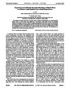
2. Hardware Architectures 2.1 Ambric The Ambric Massively Parallel Processor Array (MPPA) [4], [5] is a TeraOp System on Chip with 336 32-bit custom RISC processors physically arranged as 42 “brics.” Each bric consists of eight (four simple, four DSP) processors, 21KB of SRAM, local interconnect, and hierarchical channel interconnect. Internally, the bric is organized as 2 Compute Units, each with 2 SR (simple) and 2 SRD (DSP) processors and a RAM Unit (RU) containing 4 independent single ported RAM banks of 512 32-bit words as shown in figure 1. The interconnect implements self-scheduling FIFO communication. The RAM banks can also be linked directly to the channels to implement other types of buffering schemes of various sizes. Each 32-bit channel is capable of 9.6Gb/s, with a total bisection of 792Gb/s. The initial chip was fabricated in standard-cell 130nm, with 180M transistors, runs at 300MHz and dissipates 3W–14W depending on resource usage. Ambric’s architecture embodies in hardware the Kahn process graph programming model [12] of simple processes communicating via uni-directional boundedbuffer streams (called Ambric channels). Processes are programmed in a subset of Java, which is compiled to native machine code. Ambric’s Java subset is limited
Fig. 1: Ambric BRIC layout [4]
to bit operations, multiply, add and subtract on up to 32-bit data types. Higher level Java language features such as polymorphism are not supported. Processes compute over a combination of local state plus data read from input channels. The channels can link to other processes or to memory locations. The processors compute a new state and can also write data to output channels. The assembly instructions can read from two channels or registers, store to a register and send to an output channel in a single clock cycle. The process interconnection and parameters are described separately from the Java processor code in an “astruct” file. Thus, the programming model combines procedural processor code with declarative process interconnection description. Compilation for Ambric consists of software compilation of the Java code to native machine code followed by mapping, place, and route of each process’s program and interconnections onto the physical array. The compile time for our applications was on the order of 1-5 minutes on a 3.4GHz PC. The programming environment consists of an Eclipse framework for code development and debug, a Java functional simulator, an instruction level simulator, and a seamless transition to hardware debug.
2.2 FPGA-based Architecture For these experiments, we used an Altera FPGA on the XtremeData XD1000. The XD1000 architecture combines a dual core Opteron with an Altera Stratix
II EP2S180 on a dual socket motherboard. FPGA and processor communicate over non-coherent hypertransport on a 64-bit interface at a maximum bandwidth of 500MB/s. Our designs did not need the off-chip SRAM or DRAM accessible directly from the FPGA. The Stratix II is a 90nm integrated circuit with 180,000 logic elements, 9Mb of on-chip memory, 384 (18b×18b) multipliers and clock frequency up to 550MHz. The Stratix power usage depends on resource usage and clock frequency. For our benchmarks, it is comparable to the Ambric. Our algorithms were coded in C and VHDL, and compiled with the Impulse C compiler and the Quartus II 7.1 tool chain.
Fig. 2: Trellis decoder structure
3. Trellis Decoder Trellis coded modulation is a modulation scheme that enables efficient communication over band-limited channels with very low error rates [15]. A trellis encoder uses a rate (k/n) convolution code to map k input bits to n output bits. An additional encoder parameter is the constraint length K . The encoder produces 2n symbols that are maximally separated from each other via a Euclidean distance metric. The trellis decoder takes each symbol and reduces it back to data bits by using the Viterbi algorithm [6] which finds the most likely set of bits for each symbol received. Trellis coded modulation is a well understood technique used frequently in industry for communication applications. Our intent with the Viterbi trellis decoder module was to gain an understanding of the Ambric programming model, issues in debugging and optimization, and performance of the Ambric chip. We also implemented the decoder on the XD1000’s Stratix II in Impulse C.
3.1 Ambric Implementation The decoder built for the Ambric decodes a rate 2/3 code, with K = 5. Each state has a limited number of potential previous states, in our implementation each state had four potential previous states. Each previous state has an error associated with it. The transition error to the new symbol is calculated for each of the potential previous states. The additional error associated with the transition is added to the error of the previous states. The lowest total becomes the new state error and is fed back into the system for the next incoming symbol. The state with the lowest overall error is used as the starting point of the trace back loop. The best previous state for each state is stored in a trellis, going
back 30 states. That “best” state is used as the output state and converted back to bits. This pipelined process is followed for each incoming symbol. The decoder structure is illustrated in Figure 2. The trellis decoder data flow graph was mapped onto Ambric processes and channels. The initial process reads a 32-bit data word and parses it into individual symbols. These symbols are then written into a fanout structure that can be compiled onto the channels without requiring additional processors. The fanout feeds the symbol into each of the 16 states of the trellis decoder. Each of the state processing blocks also take in the best state errors from its four possible previous states. This creates a highly interconnected mesh in the Ambric channels, which may not be the optimal configuration but does create a effective test of the system routing resources. In addition to feeding back to the other state processors, the results are also fed into an aggregation stage. This consists of four blocks each connected to four of the processing states. The aggregation blocks combine the data into a single stream and determine the best of the four. A final aggregation stage combines the streams from the four preceding aggregation stages to a single output stream and picks the best state for input to the traceback. The traceback is implemented as a 30 stage pipeline. Each stage of the pipeline receives a best state from the previous stage, uses that data to find its own best previous state, then forwards that to the next stage. After doing the lookup, it then forwards the row of the trellis to the next stage and loads the new trellis information. In this way the channel memory is used as array storage. The active trellis is stored in registers
in the code so that no RAM is needed in the program. Channel buffers are used to prevent stalls in the output channels when transmitting the trellis to the next stage. A final stage converts the best state back to bits and collects a full 32-bit set before sending the result out of the chip and back to the host computer. The performance measurements were generated using an AM2045 GT board put in a PCIe slot on a Windows XP workstation. The AM2045 GT board is a small form factor 4 lane PCIe board. Once the program was generated the config file was loaded to the board using the SWIFT API. The SWIFT API is a C language programming interface to the ambric control, and is used for loading the programs, sending and receiving IO and querying the board status. The timing information was obtained using the windows timer API, and all tests were run multiple times to obtain an average throughput. The initial version of the trellis decoder on the Ambric was written completely in Java. Later versions implemented the entire algorithm in assembly language. The first version of the decoder showed only 35% processor utilization, and the initial throughput was 970KB/s. Subsequent optimizations were applied (see Table 1) with a final throughput of 8.47MB/s. From the time of obtaining the software to the first functional trellis decoder was about 6 weeks of half time work, which included several test programs and Hello World type applications. The various improvements to the Java code were completed over the course of the next day. The Java version 2 remapped some of the processes from SRD processors to SR processors, for a small improvement in throughput from reduced long range channel utilization. In Java version 3, some of the loop were manually unrolled. Java version 4 manually scalarized some array variables, which resulted in more than a factor of two improvement over v3. The trellis decoder was then completely re-written in assembly, for the biggest speedup, 2.65 over the previous Java version. The initial assembly language version borrowed from the available compiled Java version and optimized that code which took a further 2 days. Finally, using the instruction level simulator to track bottlenecks and stalls, we revised the assembly code to interleave operations to utilize a single cycle stall between test and branch instructions. The final optimized assembly implementation takes 33 cycles/symbol, with 4 cycles of channel propagation delay in the interconnect. This
Version SW Java v1 Java v2 Java v3 Java v4 Asm v1 Asm v2
Throughput (MB/s) .147 .970 1.006 1.327 2.79 7.396 8.47
Notes 3.4 GHz dual core x86 initial Java shift some processes to SR unroll loops use processor registers re-write in assembly use single cycle stall between test and branch
Table 1: Versions of trellis decoder Algorithm Phase Separation Processing Aggregation Find Min Trellis Bit output
Num. Cycles 4 31 23 21 20 10
Table 2: Processing time for each stage
final optimization step took an additional 3 days. All told from the initial working version to the optimized assembly code took a week. Table 2 details the number of cycles for each phase of the algorithm. The single thread software version on a 3.4GHz dual core x86 had a throughput of 0.147MB/s, giving the Ambric a speedup of 58 over software on this kernel.
3.2 FPGA Implementation Using the same high level algorithm decomposition as the Ambric design, we developed an FPGA implementation of the trellis decoder. The design was written in Impulse C for the XtremeData XD1000 platform. The design effort into the Impulse C coding was about two weeks of work, this includes about a week for the test examples and a week to do the actual coding. The design borrowed heavily from the previously completed Ambric design, and the code style was very familiar. The FPGA algorithm written in Impulse C with few hardware specific optimizations runs at 6.6MB/s at 100MHz. The theoretical max speed via simulation is 400MHz, giving a throughput of 26.4MB/s. As with the Ambric, the processing phase is the bottleneck, consuming 13 cycles compared with 33 for the Ambric. Some attempts were made at further optimization,
however due to the difficulty in compiling and testing little progress was made in the available time.
3.3 Discussion The trellis decoder benchmark was chosen as a simple, well-understood code suitable for exploring the potential of the Ambric architecture in terms of programmability, usability and performance relative to an FPGA. On both the Ambric and the FPGA, it was necessary to extract spatial parallelism from the algorithm, to apply pipelining, and to recognize and alleviate resource bottlenecks in computation and routing. The single thread software version on a 3.4GHz dual core x86 had a throughput of 0.147MB/s, giving the Ambric a speedup of 58 over software on this kernel. The FPGA version, though not totally optimized gave a further speedup of 3x over the Ambric. The raw performance numbers when comparing these processors, may not be particularly meaningful. The Ambric is a first generation chip built using older process technologies. It therefore has significant potential using modern manufacturing processes and design refinement for scaling the number of processors, reduced power consumption and faster processor clocks. On the other hand improvements in FPGA performance will depend on future technologies. The Ambric design architecture allows low level pipelining and parallel processing, and the channel mechanisms provide inherent synchronization to the many parallel paths. The individual process programming provides a natural transition from regular software design, and the hierarchical structural code provides flexibility in overall design mapping. Once the initial concepts were understood designing for the Ambric was quite straightforward. The Impulse C version of the code for the FPGA also proved simple to use and program. The design in general followed the same structure as the Ambric design and only required learning a few new function calls and techniques to write the code. To the point of simulating, the software design process was very comparable to the Ambric. However, at the stage of compiling to hardware, major differences appeared. Converting to VHDL, then linking into the Quartus system and building proved a complicated, time consuming process. Building, generating, and running a single design on the FPGA would frequently take the better part of an afternoon. In contrast, on the Ambric, a design could be built, executed, modified, and tested again many
times over the course of an hour. The rapid design cycle allowed much finer understanding of the hardware performance. Therefore problems and bottlenecks in the system were relatively easy to discover and diagnose. In contrast the long compile times on the FPGA precluded such explorations, or limited them to the software simulations. Thus, the design was much more difficult to optimize. As the number of components and processing steps in the software design increase, it is likely the advantages of the Ambric programming methodology would become more pronounced. In pure performance terms, the FPGA programmed in Impulse C outperforms the Ambric on this benchmark. In our experience, the Ambric proved much more tractable than the FPGA to debug and optimization. The Ambric’s fast design-code-test cycle and fine grained visibility into processor state made it possible to create highly optimized designs in short order. While the absolute performance lagged the FPGA, the Ambric still delivered one and a half orders of magnitude performance improvement over a modern processor.
4. N-gram Frequency Counting Calculation of n-gram frequency profiles in a document stream is a compute and data intensive kernel that has many uses. Previously, we have used this method to classify documents according to language. It can also be used in other classification problems network security for example. An n-gram is simply a sequence of characters of length n. An n-gram classifier takes a sequence of characters, extracts n characters in a sliding window, and compares the input sequence to a known profile and measures the similarity of the input sequence to that profile. In our language classification application, the n-gram frequency profile of a document is compared to known language profiles, and the most similar language profile to the input document profile determines the most probable language. One common way of calculating the n-gram frequency is with a Bloom filter [2]. In a Bloom filter, a set of hash functions generates single bit addresses into a bit vector. In training, the known n-grams are sent through the hash function and the addresses pointed to by the hash functions are set to 1. The hash functions are then applied to the data under test, and if all addressed bits contain a 1, the data is considered a match. The Bloom filter has a finite probability of false positive but will not generate false negatives.
The actual probabilities are determined by the number of hash functions and the size of the bit vector. Our implementation uses 4-byte n-grams with four hash functions applied to each n-gram. A slight variation modifies the algorithm by using a separate bit vector for each hash function and language. In embedded architectures this allows for parallel lookups and the use of distributed memory for the bit vectors.
4.1 FPGA Implementation Mapping the n-gram algorithm onto an FPGA was described in [11] and is summarized here. The ngram classification using Bloom filters was done on the Xtremedata XD1000 development system. The programming was done with VHDL. The hash functions used in the design were of the H3 family [14]. These hash codes are designed to take advantage of the programmable logic present in FPGAs and can be computed very quickly in such an environment. Dual ported embedded RAMs make it possible to apply two sets of hash generators simultaneously, enabling two ngrams to be tested in each RAM unit in each clock cycle. The flexibility of the FPGA allows the designer to take advantage of the tradeoff between accuracy and RAM usage per language. Using four 2KB Bloom filters results in a classification accuracy of 99.5%, while dropping to two 1KB filters reduces the accuracy to 95.6%. Using four 1KB filters achieves an accuracy of 99.4%. The number of languages supported is limited by the number of on-chip RAM units. For the Stratix II 180, the number of languages is limited to between 10 and 30 depending on the size of the filters used. Using the four 2KB filters allowed 10 languages to be classified and if six 512 byte Bloom filters are used, up to 30 languages can be supported. The FPGA design can accept n-grams at a rate of 1.4GB/s, classifying up to 8 per clock cycle. The maximum clock rate of the design is 194MHz.
4.2 Ambric Implementation The Ambric version of the n-gram benchmark also uses Bloom filters to count n-grams. However, the low level implementation differs significantly from the FPGA. One difference is in hash function realization. On the FPGA, the H3 hash functions are compactly represented in programmable logic, and so are duplicated along with the Bloom filters. On the Ambric,
a hash function is computed through a sequence of instructions, and a complex hash functions can consume many cycles and processors to the detriment of pipeline throughput. Therefore, on the Ambric, there is a single hash function computation unit for each branch pipeline that streams hash codes to multiple Bloom filters. In this case we trade off a small increase in the required data transmission with a reduction in required processors. 4.2.1 Hash Function In the implementation of n-gram counting, we must convert four 8-bit characters into four hash codes for the Bloom filters. In the Ambric, the simplest implementation is to use the 8-bit characters as look up addresses into the 32-bit wide local memory, using a total of 4KB (4 bytes/ngram × 256 addresses/byte × 4 bytes/word) per language. Therefore, each SRD processor can do the lookups for a single language and two languages can be implemented on a single Compute Unit. The 8-bit character specifies the address of a 32-bit word in the lookup table. To index an individual bit in the word, a 5-bit hash code is generated by a series of XOR operations on the 4 8-bit characters. First, a single 5bit hash code is generated, and then that hash code is copied and incremented three times, resulting in 4 unique hash codes. An AND operation with a bitmask is done later so that the hash codes don’t grow larger than 5 bits as a result of the increments. The increment operation is needed to ensure the ordering of specific n-grams was valid, as otherwise any byte rotation of the profile n-grams would also be valid. 4.2.2 Algorithm Overview The structure of the Ambric implementation consists of three stages shown in Figure 3. The first stage holds the system components needed to interact with the PCIe bus and the host computer. The next stage comprises the n-gram core functions for reading the data, generating the hash codes, sending the codes to the processing stages, and tallying the final results. The ngram core streams n-gram sequences and hash codes to four parallel processing pipelines. A processing pipeline is set up in a circular arrangement as in Figure 4; it consists of a head, a tail, and a series of processing blocks. The n-grams and hash codes flow in one direction and the results flow in the opposite direction to maximize the utilization of the local channels. At the end of each file the tail triggers a sequence to
Fig. 5: Ambric N-gram processing block unit
Fig. 3: Ambric N-gram design
router takes in the data for the n-gram operation from the previous block or the head, and sends it on to the next processing block. The tail of the processing pipeline sinks the data. The router then distributes the data to the Bloom filters. For each n-gram the Bloom filters perform a memory access, a bit mask generation, and a comparison for each of the four hash codes. The counter program does the final matching check on each n-gram to see if all four hash tables matched and stores the tally for each language. 4.2.3 Flexible Configuration
Fig. 4: Ambric N-gram processing chain diagram
transmit the results back up the pipeline, after which the counters are reset. Each processing pipeline consists of interconnected processing blocks (see Figure 5). A processing block performs the Bloom filter lookups, increments the match counts for n-grams that were recognized, and routes the n-gram stream on to the next processing block in the chain. A processing block uses nearly all the components in a Compute Unit (2 SR processors, 2 SRD processors, and four RAM banks). The data router and counter are implemented on the SR processors while the Bloom filters are programmed on the SRD processors. The
Like the FPGA n-gram algorithm, the Ambric algorithm is highly configurable in that the number of languages can be made to vary along with overall throughput. The algorithm has been designed such that compile time configuration options can be used to set the number of languages recognized. The astruct files (specifying stream interconnections between processes) allow conditional compilation, so the hardware is allocated in a balanced fashion automatically based on the number of languages desired. The four processing pipelines can be configured for parallel or round robin processing of the n-grams. In parallel mode, all the chains to process the same n-gram, each with a different language model. In round robin mode, all chains to hold the same language model and process different n-grams. Additionally, the processing block is capable of operating in parallel or switched operation, so it can process either two languages or a single language at nearly twice the speed.
4.2.4 Assembly Level Optimizations The coding of the n-gram classifier was done in assembly language to optimize the memory accesses and take advantage of the instruction level parallelism that is available in the Ambric assembly code. There is a delay of 3 clock cycles between sending the address to the RU channel and the availability of the data in the return channel. In assembly language it is possible in the Bloom filter code to interleave the four lookups, hash masks, and comparisons, and prevent the processor from stalling. Instruction level parallelism in the SRD was also utilized to the extent possible. For instance the code setbit | and_a RURD,bitmask,sink add_i | muxne_ca tc,1,tc generates a bitmask and computes an AND operation on the value retrieved from memory (RURD). It then increments the counter tc if the bit was set. The bitmask value is obtained from the hash code and the tc counter contains the number of Bloom filters with a match for each n-gram. This functionality executes in 2 clock cycles. It is likely many of the non time-critical functions could be implemented in Java with no loss in performance. However in this implementation, all the functions were written in assembly language for consistency, to gain experience with the processor, and to take advantage of the additional features not available at the Java language level. 4.2.5 Bloom Filter Initialization The initialization of the n-gram profiles in the Ambric is done by sending sets of integers to the Ambric. The first integer is a count containing the total number of patterns to program across all languages. Following the count, are pairs of values. The first contains the id of the language, the next contains the desired sequence. All languages are identified by id in the Ambric, numbered from 1 to N. As the initialization information flows through the core of the application, it computes the hash codes and sends that information as well. Each of the chains know which language ids it contains, so they only pass along the appropriate data for the processing blocks within the respective chains. Processing blocks check for id match and either send the data to the Bloom filters for programming or just pass it to the next block. In this manner, assuming the desired patterns are
distributed somewhat evenly among all the languages, the programming of the n-gram profiles is very fast and has been tested close to the maximum data rate of the Ambric chip for a single thread on a single channel, which in the current system is roughly 270MB/s. 4.2.6 Performance Measurements Throughput was measured using Ambric’s Swift API. This API allows the Ambric card to interact with standard C programs. The testing was done with a set of random files stored in memory to remove any influence of the disk I/O on the test. The tests were run using randomly generated 1 MB files. For each test, 1 GB of data was sent to the processor. The randomly generated files contained specific key sequences that were targeted to specific languages. This testing was sufficient to determine correct operation of the algorithm and determine the throughput. The purpose was to evaluate the algorithm operation on the Ambric as opposed to evaluating the algorithm itself (the latter was previously done in [11]). Various file sizes were tried with no discernible change in the throughput until the size got down to 10’s of bytes at which point the small amount of extra processing at the end of each file becomes a significant fraction of the required processing. 4.2.7 Channel-Related Optimizations The results of the n-gram throughput tests are shown in Table 3. Version 1 of the design used end-offile indicators and channels as flags to indicate end of document, so that the processing chain tail could transmit the results and reset the counters at the end of each file. However, this method caused a stall in the flag channel the router and counter. The bottleneck was removed by eliminating the flag channel. In version 2 the counter was initialized with the number of bytes in the document. It could then execute its loop for a fixed number of iterations and not rely on the flag channel. Setting up the loop iteration count involved sending additional information throughout the design at the start of each file but removed the channel bottleneck and increased the throughput. After the design change, the performance improved to that seen in the version 2 column of Table 3. The modification to the counter operation improved the design throughput significantly. However, there was still a significant loss in performance when moving from a single processor per language to multiple pro-
Proc/ lang 1 2 4 8
Max lang 148 74 37 18
Rate v1 (MB/s) 10.6 12.17 24.33 48.68
Rate v2 (MB/s) 15.88 17.85 35.65 71.12
Rate v3 (MB/s) 15.88 31.76 63.37 126.74
Theo. (MB/s) 16.83 31.79 63.58 127.16
Table 3: Results from n-gram classification on the Ambric
cessors. The problem was found in the sink of each processing pipeline. The sink was designed to absorb data at a rate significantly faster than the data throughput in the pipeline. No channel buffers were available in the pipeline as all the memory was required by the Bloom filters. Therefore, only a single integer buffer on the channel was available between the stages in the pipeline. The cause of the bottleneck was uneven data flow in the pipeline. Since the tail was absorbing data at a constant rate, the single buffer could cause a stall which would propagate back up the pipeline. The data was quickly absorbed but the stall still propagated back up the processing chain. The process, in effect, created an oscillation in the processing pipeline. The solution was to slow down the tail sinking pattern but match it to the data flow in the pipeline. The Ambric tools and debugging software greatly aided in locating the performance problem, particularly the instruction level simulator. The Version 3 column of Table 3 shows the final throughput results along with the theoretical performance numbers as shown by the simulator. The Bloom filters are the longest process, requiring 17 cycles in the single processor per language case and 18 in the others. The final results showed very close agreement with the theoretical results given by the simulators.
4.3 Discussion The two implementations of the n-gram frequency counting follow the same high level data flow, but diverge in the details of the compute blocks, with each striving to exploit hardware features of the respective platform. The Ambric proved fairly easy to program compared to the FPGA, and provided a great deal of visibility into operation and bottlenecks. A major advantage of the Ambric is that even using a large fraction of the resources of the chip, the total compile time of the project
was still under 5 minutes. Going from unprocessed code to running on hardware in 5 minutes allows a great deal of trial and error which is often necessary in achieving the best performance out of a system. This process is often impractical on an FPGA as the design cycle is much more involved and can take many hours for even a moderate design. With the FPGA, the designer must rely more heavily on the cycle level simulator, but such simulations can only be run on very small amounts of data. On the Ambric, testing could be performed on the actual hardware with real data, providing excellent visibility into processor and channel state. The channel communication methodology eases the burden of synchronization. However, in larger designs, minor mismatches in flow rate can cause significant performance degradations, or additional buffering must be used. For instance the mismatch in data transmission and reception patterns between the processing blocks and the processing chain tail caused a greater than 40% drop in performance even though the total data rates were compatible. Both VHDL and Assembly are low level languages that describe how the hardware operates. In both cases they require some care in development and coding and a good understanding of how the hardware they describe is structured. In the case of the Ambric, the functions can be described independently of eachother, whereas the VHDL required the programmer to define the synchronization mechanism as well, this significantly increased the complexity of the design from a software point of view. Impulse-C can take care of some of the synchronization issues but also makes the hardware specific optimizations further removed from the programmer. For this algorithm kernel, we compare two optimized implementations. The FPGA outperforms the Ambric by a factor of 11 in throughput. The Ambric showed a speedup of 9x over an efficient software implementation on an Opteron CPU. In terms of power and area the Ambric and FPGA show further improvements when compared with a CPU, though direct comparison between the Ambric and FPGA is difficult due to differences in feature size and architecture. The differences in hardware require different approaches at the low level. While the hash functions could be done in logic on the FPGA and become only a minor component, in the Ambric they consumed full processors and required many cycles to compute.
The ability to optimize and layout the processors and create higher level objects allows efficient use of the resources, to the point that it is possible to use nearly 100% of availabe resources. The Ambric represented a significant speedup over a software solution, but could not match the performance of an FPGA. However, it did prove much more enjoyable and efficient to utilize near its full potential.
productivity. In fact, with the aid of the tools and the visibility they provided into runtime operation, it was possible to optimize the design use nearly 100% of the Ambric resources. In terms of performance, the FPGA showed the best performance, outperforming the Ambric by factors of 3–11 though the Ambric had excellent performance in comparison to software in both performance metrics.
5. Conclusions
References
In this work, we investigated mappings, programmability, and performance of the Ambric MPPA in comparison to an FPGA. The trellis decoder kernel was chosen as a vehicle to compare code development effort on the two platforms from the basis of no prior experience with either technology. The n-gram frequency counting kernel further delved into the Ambric architecture. With the use of assembly code, we could create tight code sequences to minimize stalls. Detailed analysis of channel stalls led to further code optimization that balanced pipeline throughput. We note that these application kernels were chosen for their relevance to our work rather than to be well matched to a particular architecture. Both kernels map well onto FPGAs, whereas the Ambric is more suited to video and image processing where complex multistage processing is required. It also may prove very adept at handling situations with a large number of conditional processing steps, since the branching can be easily placed into the code of a single processor. Development on both platforms requires a shift in design layout from traditional sequential software to a streaming, dataflow-oriented mapping. In both cases, the mapping must take into account the hardware available in order to efficiently utilize the platform’s potential. The Ambric mapping was constrained by channel utilization considerations, the size of the embedded memories, and the instruction mix of a process’s code. On the FPGA, the sizes and ports available on embedded memories were the biggest factors, followed by efficient utilization of the lookup tables and DSP blocks. In terms of programmability, in our experience the Ambric did live up to the company’s programmability claims. The programming model was easy to comprehend and use. Compared to the FPGA, the Ambric code development environment, simulator, and debugger were also easy to use and resulted in very high
[1] K. Asanovic, R. Bodik, B. C. Catanzaro, J. J. Gebis, et al. The landscape of parallel computing research: A view from berkeley. Technical Report 183, University of California, Berkeley, 2006. [2] B. H. Bloom. Space/time trade-offs in hash coding with allowable errors. Commun. ACM, 13(7):422–426, 1970. [3] A. P. W. Böhm, J. Hammes, B. A. Draper, M. Chawathe, C. Ross, R. Rinker, and W. A. Najjar. Mapping a single assignment programming language to reconfigurable systems. The Journal of Supercomputing, 21(2):117–130, 2002. [4] M. Butts. Synchronization through communication in a massively parallel processor array. IEEE Micro, pages 32– 40, September-October 2007. [5] M. Butts, A. M. Jones, and P. Wasson. A structural object programming model, architecture, chip and tools for reconfigurable computing. IEEE Symposium on Field-Programmable Custom Computing Machines, 2007. [6] G. Forney. The viterbi algorithm. Proceedings of the IEEE, 61(3):268–278, 1973. [7] M. Gokhale, W. Holmes, A. Kopser, S. Lucas, R. Minnich, D. Sweely, and D. Lopresti. Building and using a highly parallel programmable logic array. IEEE Computer, 24(1):81– 89, Jan. 1991. [8] M. Gokhale and B. Schott. Data parallel C on a reconfigurable logic array. Journal of Supercomputing, 9(3):291–313, 1994. [9] M. Gokhale, J. Stone, J. Arnold, and M. Kalinowski. Streamoriented FPGA computing in the Streams-C high level language. In IEEE Symposium on Field-Programmable Custom Computing Machines, pages 49–56, 2000. [10] M. Gokhale, J. Stone, and E. Gomersall. Co-synthesis to a hybrid risc/fpga architecture. Journal of VLSI Signal Processing Systems, Sept. 2000. [11] A. Jacob and M. Gokhale. Language classification using ngrams accelerated by fpga-based bloom filters. In Proceedings of the HPRCTA ’07, Nov. 2007. [12] G. Kahn. The semantics of a simple language for parallel programming. Information Processing, pages 471–475, Aug. 1974. [13] D. Kissler, F. Hannig, A. Kupriyanov, and J. Teich. A highly parameterizable parallel processor array architecture. In Proceedings of the IEEE Field Programmable Technologies conference 2006, pages 105–112, 2006. [14] M. V. Ramakrishna, E. Fu, and E. Bahcekapili. Efficient hardware hashing functions for high performance computers. IEEE Transactions on Computers, 46:1378–1381, 1997. [15] G. Ungerboeck. Channel coding with multilevel/phase signals. IEEE Transactions on Information Theory, 28(1):55–67, 1982.