accepted, the data values being maintained by the sender until the ... 1 Non-return-to-zero and return-to-zero protocols are often called two- phase and ...
Asynchronous Embryonics Alexander H. Jackson & Andrew M. Tyrrell Bio-inspired Architectures Laboratory, The Department of Electronics, The University of York, Heslington, York, YO10 5DD, UK {Alex.Jackson, Andy.Tyrrell}@bioinspired.com http://www.bioinspired.com Abstract As embryonic arrays take inspiration from nature they display biological properties, namely complex structure and fault-tolerance. However, they have yet to take advantage of a further biological feature at a fundamental level; asynchronous operation. In addition to the benefits normally associated with asynchronous digital design, such as intrinsic power management, two areas in which embryonic arrays could benefit are scalability and reliability. This paper gives an overview of embryonic systems and a pertinent asynchronous methodology, that of macromodules. It is shown that a macromodule approach allows the implementation of asynchronous circuits on Xilinx Virtex FPGAs using only the standard design tools. A preliminary VHDL simulation illustrates the operation of an asynchronous embryonic array. Although mentioned, little detail of the reconfiguration scheme is given for brevity. This simulation brings truly asynchronous embryonic circuits a step closer.
1. Introduction 1.1. Biologically-inspired systems Life exhibits a number of essential properties, some of which man-made computing systems aspire to: learning, fault-tolerance, control of complex structures, and asynchronous operation. Biologically-inspired computing systems make explicit abstract use of some of these properties within their design. The POE model classifies biologically-inspired systems along three axes; phylogeny, ontogeny and epigenesis [1, 2, 3]. Ontogenetically-inspired systems are those motivated by the process of development from a genetic description. The biological result of development is an individual of
the given species, which generally has a complex structure. Whilst the cells that constitute the individual do fail, the individual is reliable because of the self-diagnosis and self-healing mechanisms present. Essentially these mechanisms are the biological equivalent of the detection and recovery stages of fault tolerance, and furthermore are distributed rather than being under the control of a central unit, as typically found in hardware systems. Reliability is paramount for systems intended for hostile or inaccessible environments, and increasingly those used by society in general. These factors imply the need for a fault tolerant capability in electronic systems, as the fundamental components cannot themselves be made entirely reliable. One noticeable disparity between the cells of biological systems and the functional units of conventional digital systems is the lack of a global signal that synchronously coordinates the activity of each and every cell. In electronic terms they are asynchronous; there is no global clock. Although asynchronous digital circuits were first studied [4, 5] at around the same time as self-reproducing automata [1], the first ontogenetically-inspired computing system, the simple design structure offered by synchronous techniques have allowed them to dominate.
1.2. Paper Structure Section 2 introduces asynchronous digital methods. Section 3 outlines embryonic systems. One method for creating asynchronous circuits using the Xilinx Virtex field-programmable gate array (FPGA) is given in section 4. The simulation of an asynchronous embryonic array is described in section 5. Section 6 concludes, and is followed by a discussion of further work.
2. Asynchronous Electronics Digital systems, both synchronous and asynchronous, assume that signals are in one of two possible states.
However, whereas synchronous systems split time into discrete, regular, intervals [4], asynchronous circuits do not use a clock. The assertion of signals, including data flow, is controlled by those parts of the circuit involved in communicating that data. Asynchronous systems can be classified by their timing model, signalling protocol, and also the method used for their design and implementation [6].
2.1. Timing Models Two timing models are of particular interest. The bounded-delay model assumes that all gates and wires have a bounded delay. The combinational logic of sequential synchronous design assumes this model. That is, there is an upper bound on the time taken for the combinational logic to produce next-state values at the inputs of the storage elements. The delay-insensitive (DI) model results from making the opposite assumption, that gates and wires have an unbounded delay. As there is no upper bound, a gate causing a signal transition cannot guarantee that it has been noticed at the receiver, implying that the gate must wait indefinitely. As this situation would be untenable in practice, a delay-insensitive gate must have some feedback path from each gate to which its output is connected. This allows the sending gate to be notified once its output has been accepted.
2.2. Signalling Protocols The majority of asynchronous circuits, notably those containing datapaths, make use of an inter-element signalling scheme. This acts as a protocol layer for both data and control transitions. These circuits are termed self-timed, as control is distributed [7]. Communicating self-timed circuit elements display the common feature of being connected by one or more closed signal paths [7]. This ensures that each element is not sent further data until it can be processed. Asynchronous signalling protocols typically use event logic. An event is a logic level transition. Both rising and falling transitions carry the same meaning, the occurrence of an event, the absolute value of the signal being of no relevance. It is implicit that a falling transition occurs after a rising transition, and vice-versa. Request Channel Parameters
Data
Number of data bits : n Total Wires: n + 2
A single-rail channel using a request/acknowledge protocol is shown in Figure 1. The data bus is like that of normal synchronous design, a single wire being used per data bit. The sender puts the data onto the bus, and then produces an event on the request line. The receiver produces an acknowledge event once the data has been accepted, the data values being maintained by the sender until the acknowledgement is received. Obviously, the data must arrive at the receiver before the request, a bounded-delay requirement termed data bundling. Data Channel Parameters Number of data bits : n Total Wires: 2n + 1
Acknowledge Sender
Receiver
Figure 2 – Dual-rail Channel
A dual-rail channel is depicted at block-level in Figure 2. Two wires are used per bit, with the data symbols following a Gray code [8], where only one of the lines changes value for every symbol sent. Implicit request control signals are therefore encoded with data during transfer. As with the single-rail system, the sender maintains its output until an acknowledgement is received. These two particulars ensure that even where the two wires of the channel introduce differing delays, the correct symbol reaches the receiver, and that no further symbols are sent until the acknowledgement has been generated. Where a channel carries a number of encoded bits, a single acknowledgement line can be used. Receive
Recover
Send
Data
Code Words Null
Data/Request
0
Acknowledge
Null
10 False
00
01
1
True
Figure 3 – Return-to-zero Dual-rail Protocol
Dual-rail channels typically use either a non-return-tozero or return-to-zero protocol1. A return-to-zero protocol is shown in Figure 3. Of the four possible two-bit values, three are used; two represent the binary logic values, the third being a null value for separating data. The fourth code word is invalid. One of the pair of bits, shown as the
Acknowledge Sender
Receiver
Figure 1 – Single-rail Channel
1
Non-return-to-zero and return-to-zero protocols are often called twophase and four-phase protocols respectively, because of the number of operational phases that exist. This terminology is avoided here as it differs from the meaning of odd (Q) and even (P) phases in the remainder of the paper.
least significant, is termed the true bit. When this is set, a logic one is being sent. The other is known as the false bit; a set state indicates transmission of a logic zero. Figure 4 illustrates a non-return-to-zero protocol, also known as a four-state protocol [8]. All four possible twobit values are used. Code Words
Receive Send
Odd Phase Even Phase
Even
Odd
P0
Data/Request
Q0
10
00
01
Q1
11
Acknowledge
P1
Parity
Data
Figure 4 – Non-return-to-zero Dual-rail Protocol
One of the pair of bits, shown as the least significant, represents the binary value of the signal. This is the data or value bit. The other is the parity or timing bit. The parity bit is set so as to make the code word contain an odd or even number of ones, resulting in odd (Q) or even (P) phase. Code words are sent with alternate phase, allowing the receiver to detect when new data has arrived.
2.3. Macromodules Macromodules are asynchronous cell library components. They can readily form self-timed circuits as their interfaces use compatible signalling protocols. Key E : Even O : Odd
Input Environment
Macromodule Pipeline
Output Environment
Reset
E
E
E
E
E
E
E
Initiation of data flow
O
E
E
E
E
E
E Time
Dual-rail data
Single piece of data
O
O
O
Data still held Single data until cleared packet moving by new even along pipeline phased data
Full
E
O
E
E Data held in each stage
O
E
E
E
macromodule about to accept data will have the same phase as that following. Initially, all stages begin with the same phase, chosen here as even. The input environment starts computation by changing the phase of its output, which also contains the first data item. The first stage accepts this, and even if no further data is input, the odd data will move along the pipeline until it is accepted by the output environment. However, as soon as the output phase of the first stage has become odd, the input environment can produce an evenly-phased output. This can be accepted by the first stage once it has passed its odd phased data on to the second stage. Hence, a pipeline that is operated at maximum rate will have stages with alternately phased outputs, except for the period where stages are communicating data. Although the macromodules of the pipeline shown only have one upstream and one downstream unit, the same principle of operation applies where a stage has multiple input or multiple output connections. One basic gate that operates in a delay-insensitive fashion is the Muller-C gate (or element) [4], named as it forms the conjunction of input events at its output. That is, a transition occurs on the single output only after one has occurred on each input, of which there are at least two. Initially the inputs must be at the same level as the output. The output will only change level when all the inputs are at the opposite level. Similarly, the output level will only change back to its initial value when all of the inputs have once again changed. Figure 6 shows the symbol, truth table and a gate-level realisation of a two-input Muller-C gate. Muller-C gates pervade asynchronous design, and are used both within macromodules and as macromodule components themselves. C B A C*
A
C
B
Acknowledge
Three input majority
E
O
E
Figure 5 – Non-return-to-zero Macromodule Pipeline
Figure 5 shows how the operation of a pipeline can easily be interpreted for a non-return-to-zero protocol [8], where the phase shown is that of the macromodule’s output. The acknowledge line is used by an upstream macromodule to determine its follower’s phase. However, as the data and request signals are encoded, downstream elements can determine their predecessor’s output phase from the dual-rail value they receive. A macromodule will only accept new data when the previous and following stages have alternately phased outputs. A
Gate-Level Design
0 0 0 0 1 1 1 1
0 0 1 1 0 0 1 1
0 1 0 1 0 1 0 1
0 0 0 1 0 1 1 1
Truth Table
A B
C
C
C* = A.B + B.C + A.C
Symbol
Figure 6 – Muller-C Gate
3. Embryonics 3.1. Inspiration VLSI circuits share features with ontogenetic systems; they have a complex structure and may need to be faulttolerant. Furthermore, the elements of array-based architectures, which are more readily integrated, are of the same type or of a small number of different types.
Embryonic (embryonic electronic) arrays [2, 3, 9, 10] draw on these similarities through the developmental process of embryogenesis, the formation of the embryo. Starting from a single cell, the zygote, the embryo is formed through cell division. By having a multicellular structure, the cells of the embryo can specialise their function; a process called cellular differentiation. Cells differentiate in the early embryo according to their relative positions, their location being determined by chemical gradients.
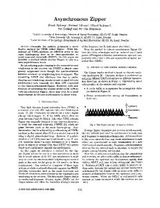
3.2. Array structure & operation The array’s processing elements are analogous to biological cells with the array providing the multicellular structure. Although the array is homogeneous, each element having identical processing capability and local neighbour interconnection, the configuration string in use determines the element function. In analogy to its biological counterpart, each electronic cell contains all required configuration strings. This complete set of configurations imitates the biological genome, a single configuration string being equivalent to a gene. As each cell contains a complete set electronic cellular differentiation can occur. In place of chemical gradients, each cell receives and sends coordinate values to its neighbours. This allows each to determine its position, and hence choose its configuration. Cellular division is emulated when the array’s cells initially have no configuration data, the complete set of configuration data being passed to the electronic zygote cell. This transmits the data to its neighbours, who in turn can do the same. In this way, all cells eventually receive the configuration set. As each cell has configuration data for every other self-repair is readily achieved in an embryonic array. The simplest reconfiguration strategy, row elimination, removes an entire row from operation when one of its members detects a fault (Figure 7).
1,4
2,4
3,4
1,4
2,4
3,4
1,3
2,3
3,3
1,3
2,3
3,3
1,3
2,3
3,3
1,2
2,2
3,2
1,2
2,2
3,2
1,2
1,1
2,1
3,1
1,1
Initial Array
x,y
Spare Cell
x,y
Active Cell
3,2 2,1
3,1
Cell (2,2) fails
Failed Cell 1,1
2,1
3,1
Reconfigured Array
Note: Logical Coordinates shown
Figure 7 – Embryonic Array Reconfiguration
The faults are detected by providing each cell with built-in self-test (BIST) logic. The cells of the failed row switch to transparently pass signals and do not increment the row coordinate value they receive. Due to this, those rows above the failed row receive new logical array
coordinate values, and switch to perform the associated task. The array can only tolerate failure of as many rows as it has spares. An embryonic array is essentially an FPGA bestowed with distributed hardware fault tolerance. By spreading the detection and reconfiguration mechanism throughout the array, the need for a centralised controller is avoided. Synchronous embryonic arrays, the type described in this section, supply a global clock signal to each cell. As the reconfiguration logic is combinational, the clock rate is selected to permit reconfiguration to complete before the next active edge, thereby allowing computation to continue [2]. Alternatively, whilst reconfiguration occurs a global signal may be used by the failing cell to indicate to the others that computation should be suspended [3]. Each cell’s processing element can be simple, such as a two-input multiplexer, or more complex, for example a microprogram processor. Multiplexer-based elements have been used extensively as these allow direct implementation of binary decision diagrams (BDDs) [2, 3]. By using a sufficient number of multiplexers, any combinational function can be realised. Through registering final multiplexer outputs, sequential circuits can also be constructed. The outputs from the final stage multiplexers need to be fed-back as next-state values. The typical approach is to provide fixed local communication between cells, with long-distance paths (‘buses’) being catered for by connecting segments of uncommitted local routing. The homogeneity of the array is maintained by integrating the routing and logic in this manner.
4. Virtex Macromodule Library 4.1. Motivation Macromodule libraries have previously been used for implementing asynchronous circuits on commercial FPGAs; effectively using a physically synchronous device to create an asynchronous FPGA [11, 12, 13, 14]. This approach is attractive due to the ready availability of commercial devices. However, as the device and tools are meant for synchronous operation a greater design and implementation effort is needed. Embryonic arrays (Section 3) have also been implemented using standard FPGAs as a physical platform [3, 10]. Therefore, as an initial step towards the realisation of a completely asynchronous embryonic array, a basic macromodule library was developed for the Xilinx Virtex FPGA. This has allowed the capability of the hardware and design methodology to be assessed. However more comprehensive macromodule-based approaches exist, such as Balsa [12, 15, 16]. The Balsa system consists of a number of tools, the first of which allows design entry through a CSP-like hardware description language. This is then translated into an
intermediate handshake circuit representation, which can be further translated into a gate-level netlist suitable for standard implementation tools. Although originally designed for use with a silicon library, more recent tool developments have allowed Xilinx FPGAs to be targeted [12, 15]. The basic macromodule library described here contains components that are designed around the specific logic resources present in the Virtex architecture, but meet the fundamental computational requirement of a multiplexerbased embryonic system. Currently only the Xilinx Foundation software tools are used for asynchronous design entry, through schematic capture, and implementation. The programmable resources of the Virtex device are termed configurable logic blocks (CLBs), and each contains two equivalent slices. A slice contains two logic cells, each having a four-input look-up table and a singlebit storage element. The latter can be configured as either a flip-flop or a latch.
4.2. Design This design makes the common choice of having the macromodules externally delay-insensitive [6], whilst their internal components operate under some other timing model. Here a bounded-delay model is chosen. As few basic gates are delay-insensitive [4], combining models allows simple circuit construction whilst retaining the advantage of delay-insensitivity at the module-level; that is the routing delay between modules does not have to be known, generally the case when implementing circuits on an FPGA. Dual-rail Inputs P
Ia
D
3-input Function Logic
D P
Ic
Q
D
Q
O
D
Parity Generator Logic
P
Ib
D
C
P Dual-rail Output
D Delay
Acknowledge Out
Event-toEdge Converter
Acknowledge In
Figure 8 - Three-input Generic Macromodule
Figure 8 shows a generic macromodule from the library. A non-return-to-zero delay-insensitive code is used. Both of the output rails are initially zero, as is the Muller-C gate output; that is the macromodule is reset to an even-phase zero, and has a low-level acknowledge output. The exclusive-OR of an input’s data and parity values generate an event when a new input value arrives. By inverting the level of the acknowledge in line, initially at logic zero, the Muller-C gate will produce a capture event once all of the input lines have received new data.
The delay allows the logic function, realised by a look-up table (LUT), to compute before the capture event causes the new value to be stored, and hence output. The new data bit’s parity value is also determined before capture from the value of the new data and the previous output phase. As Virtex flip-flops are edge-triggered, event-toedge conversion is needed. Once new data has been output, the sender or senders can be acknowledged. The capture event can be used for this purpose. Although new data may then arrive on each input the macromodule cannot make use of it until it has received an event on the acknowledge in line, as its output may otherwise not have been received.
4.3. Implementation The unintentional introduction of hazards must be avoided when using standard FPGAs for asynchronous circuits. Hazards are not problematic in synchronous design because the clock updates variables after glitches have passed. However, hazardous logic along an asynchronous circuit’s control line could lead to undesired, misinterpretable, transitions. All lines are involved in control where macromodules communicate using DI channels. The only potentially hazardous logic in the generic design (Figure 8) is the functional logic and parity generator. The Muller-C gate is hazard-free if no input transition is rescinded before the corresponding acknowledgement is received by the sender. This will always be the case, assuming that the signalling protocol is followed and that the feedback line is short. The Muller-C gate’s feedback line (Figure 6) must have fixed the new output state before another gate responds to the event produced. The local CLB routing provided by the Virtex architecture allows this to be the case. Hazards are avoided by the same technique used in synchronous design; flip-flop capture does not occur until the function logic and parity generator have settled. The capture event delay must meet or exceed the function logic’s delay bound. By encapsulating the bounded-delay logic inside macromodules, routing management is eased considerably. However, as the tools are intended for synchronous operation a number of different techniques are used to ensure that routing constraints are met. Although little direct control over routing is possible, routing is affected by placement, a factor that is readily controlled. This is useful in a number of ways. The data and capture paths (Figure 8) both start from the same, known, location if the functional look-up table and exclusive-OR gates are placed in the same CLB. The capture path can then be routed through a sufficient amount of otherwise unused logic. This typically results in the capture event delay exceeding the delay-bound of the data and parity bit calculation.
Look-up tables, three-state buffers, and in particular storage elements, are used to realise the delay elements within macromodules. These are designed to give a delay having a lower-bound. Upper bounds can be imposed providing storage elements are used. By judicious selection of a synchronous inter-register timing constraint, a maximum path delay between the data ports of the storage elements can be enforced, even though no clock is actually used. Other asynchronous implementation methods, such as Balsa [12, 15], rely on timing simulation to check data bundling and bounded-delay constraints, and for setup and hold timing violations. Timing simulation should also be used to check for correct operation of circuits constructed from the basic macromodule library described here. Although the design methodology is applicable more generally, as the library itself is specific to the Virtex architecture it gains some benefit from the synchronous static timing analysis tools. During library construction, each macromodule component was individually implemented, its inputs and outputs being routed to neighbouring CLBs. The delay elements within the macromodule were then manually adjusted using static timing information to allow for all operating conditions. Confidence of correct macromodule operation in circuit designs is provided as the same internal routing paths are likely, although not certainly, to be used.
4.4. Test System An eight-bit asynchronous adder system has been implemented to test the macromodule library. By virtue of the design, simply changing the look-up table content alters the function performed. Therefore, full-adder blocks are built from two generic macromodules, one to implement the sum and another the carry. The eight-bit adder system reads pairs of values in sequence from two on-chip memories and places the sum of each calculation into a further memory. A host computer initially stores the on-chip values, and is responsible for reading back the calculation results. The same design principles were used to build the more complex macromodules that read and write values to and from on-chip memories for the adder. These macromodules also provide conversion between standard and dual-rail values. The host computer brings the system reset low to indicate that computation can begin. However, to allow the asynchronous computation to take place, the macromodule used to read from memory initially retrieves the first stored value and converts it into an odd-phase data output; it acts as an input environment to the adder itself (Figure 5). The asynchronous adder, if it were part of a bigger asynchronous system, would operate at about one-third of
the speed of a similar pipelined synchronous adder. It also uses about six times the amount of logic. This is not unexpected as the Virtex FPGA is intended for high-speed synchronous circuits. The synchronous adder benefits from the logic cell architecture and from having dedicated carry-routing. Furthermore, the macromodule design is not optimal for the adder system’s wide datapath. Asynchronous performance is limited by the implementation methodology in comparison to that available were greater control of routing possible. The macromodule library provides one means of implementing asynchronous circuits using the Virtex FPGA and indicates that completely asynchronous embryonic arrays are feasible. Even though the internal design of the macromodules requires detailed knowledge of the hardware architecture, the macromodules themselves are easily assembled to form asynchronous systems.
5. Asynchronous Embryonics 5.1. Benefits Asynchronous methods have the potential to benefit embryonic arrays in a number of ways. The first is that an important property of biology will be brought to ontogenetically-inspired electronic systems. Although the field programmable processor array [17], a coarse-grain array of eight-bit processors, uses asynchronous communication, embryonic architectures have yet to exploit asynchronous techniques at a fundamental level. As asynchronous operation has already been successful in other biologically-inspired systems, such as cellular computing [18] and EHW [19], and since asynchronous FPGA methodologies exist [6, 13, 14], fully asynchronous embryonic circuits are not without precedent. Asynchronous techniques are of benefit to scalability and reliability, two areas with which embryonic architectures are intimately linked. Whilst embryonic architectures provide a means of configuring massively parallel systems, a centralised clock may cause scalability problems such as clock-skew. Asynchronous design inherently avoids this. Reconfiguration is vital for the reliability of all hardware fault-tolerant architectures. Self-timed systems can simply stop sending data whilst they reconfigure, as data is not expected at regular intervals. Embryonic architectures feature distributed reconfiguration, preventing the need for a centralised controller. This mitigates problems with a single point of failure. Asynchronous design takes this one step further by replacing the centralised clock with distributed sequencing control. Additionally, embryonics can benefit from the advantages normally associated with asynchronous methods. By removing a constantly switching clock
signal, the gates of macromodule circuits will only switch when processing. As soon as data does not arrive they automatically stop, intrinsically providing low power consumption whilst not in use. Clock signals cause a large current to be drawn following the active edge as all gates switch simultaneously. Asynchronous designs have their switching transitions more evenly distributed in time, which may reduce electro-magnetic interference. Modular asynchronous designs also allow sub-systems to be interconnected without the need for clock matching at any level, assuming that they have compatible interfaces. Indeed, the simplicity of interfacing can also be of benefit for module-reuse, an important issue for all large array systems, such as state-of-the-art FPGAs. Whilst the asynchronous system of section 4 has a lower performance and higher resource requirement than a synchronous design, a recent asynchronous processor core has proven to be competitive when compared to its synchronous counterpart in terms of power, area and performance [16].
5.2. Preliminary Design A VHDL simulation of a preliminary embryonic array has been created. The simulation is behavioural only at the lowest level, as was that of the macromodule library, giving every confidence that a practical asynchronous embryonic array can be built in a similar way to the current macromodule library. The design described here does not feature reconfiguration logic for brevity, although this is mentioned in section 7. Nevertheless, each cell of the array contains a complete set of configuration strings with the operative configuration being selected by its coordinate, giving cellular differentiation. NIBUS
NOBUS
NOUT
C
WIBUS
Switch Block
EOBUS C C
WOBUS C
EIBUS
Functional Unit
WIN
SIN (INT)
C
C
WOUT
SIBUS
EIN
SOBUS
EOUT
SIN
Figure 9 - Cell Structure
Following previous architectures [2, 3], Figure 9 depicts the cell structure considered in this paper. This routing pattern is highly suited to BDD implementation. This asynchronous embryonic cell requires a total of eighteen configuration bits. The inputs and outputs are
referred to by compass point. The south input feeds the functional unit, but also the west and east neighbours. The switch block uses multiplexers to allow routing of any input bus to any output bus, except that sharing its compass point. As with synchronous designs, the switch block needs a total of eight configuration bits [2, 3]. The functional unit output is always locally routed to the north, but can also be connected to any of the bus outputs. The south buses can act as inputs to the functional multiplexer (Figure 10), whose selection line is always under the control of one of the east buses. The fundamental design changes at this level are the need for two-bit wide buses and the acknowledgement lines. Muller-C gates are necessary to combine the acknowledgement of both receivers where a bus or local connection splits. The switch block also contains multiplexers allowing self-acknowledgement when an incoming bus is not in use, as described below for the functional unit. The structure of the functional unit is shown in Figure 10. Even though a return-to-zero protocol has been adopted here, the operation remains similar to that of the macromodule library. An event-to-edge converter is not required and OR gates are used to produce an event when an input arrives. Whilst the use of this protocol may affect performance through the need for null symbols, it isolates the storage flip-flop from the output, something that cannot easily be done with a non-return-to-zero protocol. Since the output encoding logic is simple, and the transistor count for a Muller-C gate is around half that of a D-type flip-flop with preset and clear inputs, the design at present assumes that only the flip-flop will incur a fault. By returning to a zero output before each new piece of data is sent, provision is made for BIST logic to prevent the symbol from being transmitted when an erroneous value has been stored in the register. The functional unit requires a configurable Muller-C gate, as a maximum of three of the eight incoming sources are used at once. A Muller-C gate’s input is effectively removed by feeding it with the inverted output. Further multiplexers self-acknowledge those incoming sources that are not in use. This is necessary, for example, where the functional multiplexer uses EIBUS, but EOBUS carries other data. The cell transmitting data along EOBUS must be acknowledged by each potential receiver because of the Muller-C gates that lie along its acknowledge line (Figure 9). Although the selfacknowledge multiplexers are controlled by the configuration, they do not require configuration bits themselves. Their state can be determined from simple functions of existing configuration bits.
Dual-rail Cell Value Storage
1 0
NOUT D
1 0
Source Multiplexers
Q
Output Encoder
0 1
Functional Multiplexer
Ack. Line 0
1
0
1
0
A
1
S EOBUS
Delay
EIBUS SIN (INT) EIN WIN
C
NOUT
Delay
two-bit up/down counter and the asynchronous equivalent of a frequency divider. (Ortega-Sánchez [2] shows the BDD for the synchronous version of this circuit, and for the two-bit counter). Figure 11 illustrates the multiplexer diagram for the frequency divider. The synchronous design provides one output pulse every n clock cycles. Evidently an additional input is needed here as there is no global clock in this circuit. C*
Delay
Z
S
SIBUS
C*
0
C
: Configuration Multiplexer A, S : Configuration bit identifier
Figure 10 – Functional Unit Structure
The initial register value and configuration bits ‘A’ and ‘S’ are zero for most cells. The Muller-C gate’s initial output is also zero. The functional and source multiplexers, which are identical to those of a synchronous design, are assumed to have a bounded-delay. Once data has arrived on each of the inputs in use, the Muller-C gate produces a rising transition that stores the output of the functional multiplexer. In turn, this raised logic level activates the output encoder to send the data downstream, whilst also acknowledging the cell’s senders. The MullerC gate’s output switches to a low logic level only when the senders have all removed their data and all receivers have acknowledged. This makes the functional unit output revert to a null symbol, and produces a falling transition on the cell’s acknowledge outputs to complete the return-to-zero communication cycle. As embryonic circuits can form sequential systems, some cells will be contained within the next-state loop. One of the cells within the next-state loop must act to initiate asynchronous operation. Without this the external inputs will not cause computation to propagate to the output. The configuration bit ‘S’ allows the cell to initially output a data symbol. The state of the incoming acknowledge line must then become non-inverted for correct operation. Similarly the connection order of the flip-flop and output encoder are also reversed, as the output symbol must be null before a new value is stored in the flip-flop. Additionally, where a cell’s output drives one of its own inputs the configuration bit ‘A’ allows the outgoing acknowledge level to be inverted. This occurs in the two-bit counter circuit below, and is necessary as the outgoing acknowledge connects to the same cell’s incoming acknowledge.
5.3. Simulation Results Two designs, both previously used as example circuits for synchronous embryonic arrays, have been simulated; a
Zero Detector
B*
A*
A*
0 1
1
SOBUS
B*
0 1
B
‘0’ 0 1
0 1
0 1
‘0’
‘0’
0 1
3 Bit Counter
‘1’
A
0 1
0 1
‘1’ ‘0’
‘1’
System Inputs : I, V0, V1, V2 System Output : Z
‘0’
A
B
C
0 1
0 1
0 1
0 1
Z
A* V0
B* V1
C* V2
Input Multiplexers n10 = V2V1V02
I
Figure 11 – Frequency Divider
The asynchronous equivalent produces an output for each data item received on the ‘I’ input, the value of the data being unimportant. The output, ‘Z’, is a stream of encoded zero data values interspersed with an encoded one once every n inputs. Figure 12 shows a simulation output for the frequency divider. The parenthesised waveforms are formatted versions of their corresponding waveform. These display the decoded dual-rail value and do not revert to a null state for clarity. The divider value ‘n’ is the aggregate value of the divider input (V2,V1,V0). As with other dual-rail systems, it can be seen that all inputs must observe the protocol and send a code symbol, even when the data value has not changed. Figure 13 illustrates the asynchronous two-bit up/down counter operation. Again, the two output bits are combined as a decoded value for clarity.
6. Conclusion An overview of synchronous embryonic architectures has been given. It has been noted that these array architectures display some of the essential properties of biological systems, namely fault-tolerance and a complex structure. It has been observed that embryonic systems have not yet used asynchronous techniques at a fundamental level.
V0 V1 V2 I Z (n) (I) (Z)
Figure 12 – Frequency Divider Simulation Up/Down Output - B Output - A (Up/Down) (Count Out)
{ { { { {
Figure 13 – Two-bit Up/Down Counter Simulation Up/Down {
IBUS(1)
Output - B {
T O(1)
Output - A {
T O(2)
(Up/Down) { (Count Out) {
T
CONFIG (1,1) CONFIG (1,2) CONFIG (1,3) CONFIG (1,4) CONFIG (1,5) COORD_Y (1,1) COORD_Y (1,2) COORD_Y (1,3) COORD_Y (1,4) COORD_Y (1,5) 0
100 ns
200 ns
300 ns
400 ns
500 ns
600 ns
700 ns
800 ns
Figure 14 – Two-bit Counter Reconfiguration
The clock is a centralised aspect of embryonic circuits that is inherently removed by the use of asynchronous logic. Scalability and reliability have been identified as two areas where an asynchronous approach could be of benefit. In addition, advantages normally associated with asynchronous design, such as simple power management, may be realised. Techniques applicable to the implementation of asynchronous electronic circuits using commercial FPGAs have been described. Notably, asynchronous macromodules have been identified as an approach compatible with the needs of embryonics, from both architectural and implementation viewpoints. The delayinsensitivity offered by dual-rail encoding is advantageous as routing delays do not then affect correct operation. The macromodule library presented offers one means of creating asynchronous circuits using the Virtex FPGA. A preliminary VHDL simulation has shown the operation of an asynchronous embryonic array although the reconfiguration strategy had not been described. This
simulation is a major and necessary step toward the implementation of truly asynchronous embryonic circuits.
7. Further Work Although not detailed here the simulation includes reconfiguration logic. Figure 14 shows the counter reconfiguring. A fault occurs in cell (2,1) at time 450ns, with reconfiguration occurring a short while later. The address coordinates and cell configurations for the first column are shown changing appropriately. As with previous embryonic arrays [2], this design produces data output values that do not follow the count sequence during reconfiguration, although correct asynchronous protocol is observed. The formatted value shown is incorrect during part of the reconfiguration phase because of the method used to update its simulation value. The array is initialised following reconfiguration, so although normal operation resumes the count sequence is reset. The performance of asynchronous macromodules built using the techniques described in this paper would improve if more advanced control of routing were
available. It should be possible to increase implementation efficiency through use of the Xilinx JBits application program interface, which allows manipulation of the FPGA configuration bitstream. A more direct control of routing could also facilitate the use of single-rail protocols, removing the need for dual-rail conversion logic. This would be of benefit as it would counteract the unavoidable increase in cell logic caused by asynchronous design. Other implementation alternatives may be considered, such as the Balsa system [12, 15]. Further advances could also result from looking more closely at biological cell communication. Bradley et al. [20] note that address generator or configuration register faults could lead to incorrect logic and routing configuration, and that testing for this is similar to self/non-self discrimination in the immune system. The same source indicates that biological cells do not self-diagnose but rely on the immune system. This is in contrast to typical embryonic cells that contain BIST logic. Approaches that combine immunotronic ideas would be a step closer to the biological reality and by having a separate checking network embryonic cells would avoid the otherwise necessary replication of their functional circuitry.
[7] [8]
[9]
[10]
[11]
[12]
[13]
[14]
Acknowledgements This work is supported through the Engineering and Physical Sciences Research Council, UK and Xilinx, Inc. “Xilinx” and “Virtex” are registered trademarks and “Foundation”, “Logic Cell” and “JBits” are trademarks of Xilinx, Inc.
[15]
[16]
References [1]
[2]
[3]
[4] [5]
[6]
Sanchez, E. et al. (1997), "Phylogeny, ontogeny, and epigenesis: Three sources of biological inspiration for softening hardware", Evolvable Systems: From Biology to Hardware, Proceedings of 1st International Conference (ICES96), Lecture notes in Computer Science, 1259, 3554, Higuchi, T. et al. (eds.), Springer-Verlag. Ortega-Sánchez, C. A. (2000), "Embryonics: A Bioinspired Fault-tolerant Multicellular System", D.Phil. Thesis, Bio-inspired and Bio-medical Engineering, The Department of Electronics, The University of York: 159. Tempesti, G. (1998), "A Self-Repairing Multiplexer-Based FPGA Inspired by Biological Processes", Ph.D. Thesis, Logic Systems Laboratory, Computer Science Department, Swiss Federal Institute of Technology: 166. Hauck, S. (1995), "Asynchronous design methodologies: an overview", Proceedings of the IEEE, 83(1): 69-93. Davis, A. & Nowick, S. M. (1997), "An Introduction to Asynchronous Circuit Design", University of Utah Department of Computer Science report, UUCS-97-013: 1-58. Brunvand, E. (1995), Introduction to Asynchronous Circuits and Systems, Tutorial, 2nd Working Conference
[17]
[18]
[19]
[20]
on Asynchronous Design Methodologies, South Bank University, London, UK. Seitz, C. L. (1980), "System Timing", Introduction to VLSI systems: 218-262, Mead, C. et al. (eds.), Addison-Wesley. McAuley, A. J. (1992), "Four state asynchronous architectures", IEEE Transactions on Computers, 41(2): 129-42. Mange, D. et al. (2000), "Toward robust integrated circuits: The embryonics approach", Proceedings of the IEEE, 88(4): 516-43. Ortega, C. & Tyrrell, A. (2000), "A Hardware Implementation of an Embryonic Architecture Using Virtex FPGAs", Evolvable systems: from biology to hardware, Proceedings of 3rd International Conference (ICES2000), Lecture notes in Computer Science, 1801, 155-164, Miller, J. et al. (eds.), Springer-Verlag. Brunvand, E. (1993), "Using FPGAs to implement selftimed systems", Journal of VLSI Signal Processing, 6(2): 173-90. Bardsley, A. (2000), "Implementing Balsa Handshake Circuits", Ph. D. Thesis, Department of Computer Science, Faculty of Science & Engineering, The University of Manchester: 187. Maheswaran, K. (1995), "Implementing Self-Timed Circuits in Field Programmable Gate Arrays", M.S. Thesis, Electronic and Computer Engineering, University of California - Davis: 136. Payne, R. (1997), "Self-Timed Field Programmable Gate Array Architectures", Ph.D. Thesis, Institute for Computing Systems Architecture (ICSA), Division of Informatics, University of Edinburgh: 270. Bardsley, A. & Edwards, D. A. (2000), "The Balsa Asynchronous Circuit Synthesis System", Forum on Design Languages (FDL 2000). Furber, S. B., Edwards, D. A. & Garside, J. D. (2000), "AMULET3: a 100 MIPS Asynchronous Embedded Processor", Proceedings of IEEE International Conference on Computer Design: VLSI in Computers and Processors (ICCD2000), 329-334, IEEE Computer Society. Nussbaum, P., Girau, B. & Tisserand, A. (1998), "Field programmable processor arrays", Evolvable Systems: From Biology to Hardware, Proceedings of 2nd International Conference (ICES98), Lecture notes in Computer Science, 1478, 311-322, Sipper, M. et al. (eds.), Springer-Verlag. Sipper, M., Tomassini, M. & Capcarrere, M. S. (1997), "Evolving Asynchronous and Scalable Non-uniform Cellular Automata", Proceedings of the International Conference on Artificial Neural Networks and Genetic Algorithms (ICANNGA97), 66-70, Smith, G. D. et al. (eds.), Springer-Verlag. Thompson, A. & Layzell, P. (1999), "Analysis of unconventional evolved electronics", Communications of the ACM, 42(4): 71-9. Bradley, D., Ortega-Sánchez, C. & Tyrrell, A. (2000), "Embryonics+immunotronics: a bio-inspired approach to fault tolerance", Proceedings of 2nd NASA/DoD Workshop on Evolvable Hardware, 215-233, Lohn, J. et al. (eds.), IEEE Computer Society.