The test vector generation with constraints (for digital circuit) and fault ...... 96-101. [13] A. Meixner and W. Maly, âFault modeling for the testing of mixed inte-.
Automatic Test Vector Generation for Mixed-Signal Circuits Bechir Ayari, Naim BenHamida and Bozena Kaminska Ecole Polytechnique of the University of Montreal P.O. Box 6079, Station “Centre-ville”, Montreal, PQ, Canada, H3C 3A7
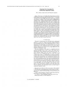
Primary Outputs
Digital
Testing a mixed-signal circuit means finding out if the circuit meets some of its specifications. So, the problem of mixedsignal testing is to convert the parameter specifications from the analog domain to the digital domain. In order to propose a test strategy for a mixed circuit, a testing technique for every block of the circuit is needed. The element testing technique will be used for analog circuits [8]. For the digital circuit an automatic test vector generation technique based on BDD and boolean difference will be used as described in [10]. To test an analog-digital circuit, Figure 1, the digital block should be tested under the conditions imposed by the analog block. The effect of a faulty element in the analog block should be propagated through the digital block. The analog part of the A/D converter is considered as a part of the analog block and the digital part is considered as a part of the digital block. For the digital block, the constraints imposed by the analog and conversion blocks are taken into account in the testing procedure.
ADC
Recent improvements in fabrication technology have made possible the realization of reliable integrated circuits (ICs) containing both analog and digital functions on the same silicon chip. The problem of testing these circuits is, however, much more complicated than that of testing purely digital or analog ICs. The testing demands for each type of circuit are somewhat different. Digital circuit testing, very crudely, consists in checking that the pattern of 1’s and 0’s at the outputs corresponds to the pattern expected. Analog testing consists in measuring, for example, gain, bandwidth, distortion, impedance, noise, etc. So, different techniques have evolved for the two types of circuits which are difficult to integrate into a single testing solution. Because the problems mentioned above are difficult to handle, generically specific solutions for standard mixed circuits such as CODECs [1], ISDN [2] and A/D converters [3] have been proposed. The other alternative is the use of Design For Testability (DFT) rules, that basically partition the mixed circuit into analog and digital sections so that the input and output signals of each section can be accessed. One possible implementation of this technique is the use of some analog and digital multiplexers for controllability/observability purposes [4] and [5]. A possible implementation is the use of the mixed-signal test bus standard IEEE P1149.4 [6]. Using this method, both chip area and the number of I/O pins will have to increase to accommodate the test requirements. Alaa et al.[7] presented a steady-state-response test generation method for mixed-signal integrated circuits. This technique considers catastrophic faults only. Also, the circuit should be modified before being tested by this technique. In this paper, a new test method for mixed-signal ICs is presented. The circuit is considered as an entity, so there is no need for circuit partitioning into analog and digital blocks. The proposed test generation technique consists of functional testing for the analog parts and test vector generation with constraints for the digital parts. This technique allows the test of every block under the conditions imposed by the other blocks. For purpose of consistency only the case of analog-digital circuits is considered, Figure 1. Other configuration type of a mixed circuit is the subject of another paper.
2. Analog-digital circuit testing
Analog
1. Introduction
The rest of the paper is organized as follows: in section 2, the testing procedures for the analog circuit is first reviewed. The test vector generation with constraints (for digital circuit) and fault propagation from one block to another are then presented. Some experimental results are discussed in section 3. A conclusion is given in Section 4.
Primary Inputs
Abstract Mixed circuit testing is known to be a very difficult task. This is due to the difficulty of: testing the analog part of the circuit, controlling the digital signal from the analog outputs, observing the analog outputs in the digital circuit, controlling the analog circuit from the digital outputs and observing the digital signals in the analog circuit. As a solution to these problems, we propose an automatic test vector generation for mixed circuits to perform functional testing. In this paper, a case of an analog block followed by a digital block is considered. The experimental results (simulation and discrete realization) show the efficiency of the automatic test generation technique.
Figure 1: Analog-digital circuit
2.1 Test method for analog circuits Faults in analog circuits can be categorized as catastrophic or parametric (soft). Catastrophic faults are open and short circuits caused by sudden and large variations in components [9]. Parametric or soft faults are defined by the circuit’s functionality. In analog circuits, the concern is which parameters to select for testing and the accuracy to which they should be tested in order to detect the variations in the faulty components. We know that the circuit’s parameters depend on the circuit’s elements, and finding a test set for the elements of the circuit consists in finding a set of parameters to be measured that guarantees maximum fault coverage of the elements. The maximum fault coverage of an element is defined as the minimum element deviation that can be observed by measuring one parameter. The element coverage is defined as the minimum element deviation that can be observed at one primary output parameter at least. To quantify the coverage of an element, we should compute the relative deviation of the faulty
element, and, where the other elements are fault-free, their tolerances are taken from the circuit’s technical notes. The test vector generation method proposed here is based on graph modeling presented in [8]. Graph modeling reduces the complexity of the relation between input and output, and also overcomes the nonlinearity of the system. Another advantage of graph modeling is that we can transform the problem of analog circuit testing to a known flow problem in graph theory. As a test strategy, we build a circuit graph, and then we compute the element’s relative deviation. There are two kinds of element’s relative deviations: The first is the relative deviation of a fault-free element, which is taken from the circuit’s data sheets. The second is the faulty element relative deviation; in this case the worst element tolerance is computed. For every parameter that depends on the faulty element xi , the maximum value of the tolerance of element xi is computed, and the other elements are assumed to be fault-free. Once all the element tolerances have been computed, another weighted graph is constructed. This graph is a bipartite graph that relates primary output parameters and elements. The graph problem obtained can be solved by choosing the best parameters to test the elements. More details about this technique can be found in [8]. 2.1.1 Example 1
The second order band-pass filter, Figure 2, is used to illustrate the testing procedure for analog circuits. The second order band-pass filter has eight elements {R1, R2, R3, R4, Rg, Rd, C1, C2} and five parameters: A1: center-frequency gain, A2: gain at 10khz, f0 : center frequency, fc1 : low cut-off frequency and fc2 : high cut-off frequency.
) E = { (PI ,PI ,… ,PI 0 1 n−1
R1 C2 R3
A3 +
) E = { (PI ,PI ,… ,PI 0 1 n−1
Figure 2: A second order band-pass filter
We consider that parameter tolerances are equal to 5%. Also, an element is considered fault-free if its tolerance is less than or equal to 5%. The worst-case deviation is computed for all the elements and each parameter, equation 1. A1 and A2 constitute the test set for the analog circuit. If A1 is measured, a deviation in Rd greater than 9.9% can be detected. In fact, this deviation will force A1 out of its tolerance box. \ R1 R2 R3 R4 Rg Rd C1 C2 A1 0 0 0 0 10.1 9.9 0 0 A 2 28.9 28.9 28.9 28.9 176 176 27 28.9 f 0 36.3 36.3 36.3 32.2
0
0
36.3 36.3
f c1 44.5 44.5 44.5 37.2 37.2
0
40.4 38.3
f c2 30.5 30.5 30.5 40.1 40.1
0
28.7 30.5
f ⋅ F ⋅ PO = D l c l=D
represents the set of test vectors for the fault l s-a-0 that satisfy the constraints, and
R4
A2 +
S = f ⋅ F ⋅ PO = D or l c l=D
S = f ⋅ F ⋅ PO = D or f ⋅ F ⋅ PO = D} l c l=D l c l=D
represents the set of test vectors for the fault l s-at-1. Example 2: Consider the circuit of Figure 3, where the lines l0 and l2 of the digital circuit are connected to Va and Vb respectively. Vdd Rc1 Vt1 Vd Rc2 Vt2
+ Va Co1 + Vb Co2 -
DFF
~
Rd R2 A1 + Vout
DFF
C1 Rg
propagate the resulting error to a primary output (PO). But, generally, in a mixed circuit, many lines of the digital part are controlled by the same analog signals. This will create dependency between some of the inputs of the digital circuit. Then, many assignments to the digital circuit lines cannot be obtained by controlling the analog signals of the circuit. As a result, while activating or propagating the fault, the assignment to circuit lines must satisfy the constraints. Then the question that rises is: How can we take into consideration constraints brought about by the analog part? The digital circuit inputs connected to the analog block must take assignments that can be obtained by controlling the analog signal. These assignments are represented by a boolean function called Fc (constraint function). In our approach, Fc is a sum of product terms represented by an OBDD. Each product term represents an allowed assignment to the lines depending on the analog part. Then, any assignment that makes Fc equal to 1 can be obtained by controlling the analog signal. Note that if all the assignments are allowed, Fc will be equal to 1. As a result, there is no constraint to satisfy while generating test vectors. If we try to find an assignment to activate the fault and after that see if the fault can be propagated to a PO, we will find that in many cases, a great deal of backtracking will be required. By manipulating boolean functions, we can avoid backtracking and obtain directly the set of test vectors that activate the fault, propagate the error and satisfy the constraints at the same time. Then, for a mixed circuit, the test vector (assignments to PIs) must satisfy 3 conditions: 1) activate the fault, 2) propagate the fault to a primary output, and 3) satisfy the constraints imposed by the analog part. For example, the set
l0 l1 l2 l4
Rc3
l6 l5 l7 l3 f s-a-0 l8
l9 Vo1 l10 Vo2
(1)
This testing procedure allows us to test the faults inside the operational amplifier (OpAmp) by choosing the appropriate model of the OpAmp. The models of OpAmps presented in [12] and [13], that consider all possible faults, can be used for this purpose. 2.2 Test vector generation with constraints 2.2.1 Test vector generation using OBDDs
In the approach presented in [10], an algebraic method based on OBDD representation is used. For the digital circuit, the fundamental steps in generating a test vector for a fault l s-a-v (v=0 or v=1) are, first, to activate (excite) the fault, and, second, to
Figure 3: A two-output circuit with the fault l3 s-a-0
In this case, the logic value of l0 and that of l1 will be controlled by the same analog input. As a result, these two lines become dependent. Note that we cannot control these lines to zero at the same time. Suppose also that we have to generate a f = l2 , test vector for line l3 s-a-0. Then, l3 Vo1
l3 = D
= ( l2 + l1 ) ⋅ ( l0 + D )
this example,
F = l0 + l2 c
and fl3 ⋅ Vo1l3 = D = l1 ⋅ l2 ⋅ ( l0 + D) . For (l0=0 and l2=0 cannot be obtained).
Consequently, S = fl3 ⋅ Fc ⋅ Vo1l3 = D = l1 ⋅ l2 ⋅ ( l0 + D) . Note that S = D only when l0, l1 and l2 are equal to 0, 0 and 1 respectively. Then, the test vector { l0, l1, l2, l4} = { 0, 0, 1, X} tests the fault and satisfies the constraints. When considered alone, the digital circuit of Figure 3 is found to be fully testable, which means that 100% coverage
can be obtained. But, when it is a part of the mixed circuit, the fault coverage will change. The dependency introduced by the analog part have an effect on the fault coverage of the digital block. For this circuit, we have found that 2 of the 18 uncollapsed single stuck-at faults considered become undetectable when both circuits are connected. Note that the faults l0 s-a-1 and l3 s-a-1 cannot be tested, since lines l0 and l1 cannot be controlled to 0 and 0 respectively. 2.3 Analog fault activation If we apply a signal in the analog primary input, all the PIs of the digital part controlled by this analog input will have a logic value equal to 0 or to 1. Suppose that we have to generate test vectors for the analog parts of the mixed circuit in Figure 4. In this circuit, we have supposed that we have only one analog input. Suppose that we have a faulty component in the analog part of the mixed circuit. In other words, the element deviates from its specification tolerance. To activate the fault, the parameter from which the element should be tested is chosen. In order to propagate the fault through the conversion block, the signal to be applied in the analog primary input must force at least one output of the A/D converter to have a different value in the fault-free circuit and in the faulty one. Suppose that a parameter is considered faulty, due to an element deviation, when its deviation exceeds 5%. The analog input should be chosen such that we have an output of the A/D converter that has different values when the parameter deviation is inside the tolerance box [-5%,5%] and when it is outside the tolerance box.
Rd
Ia
Mixed Circuit
Vdd A/D Va
l0 l1 Vb l2 l4
Va Analog
Digital
Primary Outputs
Primary Inputs
∆ T
Figure 4: Mixed-signal circuit
To test any element/parameter of the analog circuit, the amplitude A and the frequency f must be chosen appropriately. The circuit of Figure 5 will be used as a vehicle to introduce the test vector approach. To activate a fault, we must have different logic values at the output Vd of a comparator of the conversion block. Table 1 gives, for each parameter to test, the corresponding amplitude and frequency of the signal which should be applied to the analog circuit. The techniques for choosing the amplitudes and frequencies ( depending on the cut-off frequencies of the analog circuit) are described in [8]. ∆ T To test a parameter T deviation ( ), two vectors are needed, T
one to test the upper bound of a parameter deviation and the other to test the lower bound, Table 1. A parameter T is considered fault-free if its deviation is ∆ T inside the tolerance box [-x,+x] ( ∈ [− x, + x] ), otherwise it is T
faulty. Table 2 gives the notation of the used parameters. signal(A,f)
Analog Circuit
Va Vref
Vd
Figure 5: Analog-digital circuit
Digital Circuit
Test
f
A > DC ( 1 + x) ⋅ A A
DC
β
A < DC ( 1 − x) ⋅ A
DCn
> AC ( 1 + x) ⋅ A
V ref ( 1 + x) A
0
DCn
AC
A < AC ( 1 − x) ⋅ A
> lcf ( 1 + x) ⋅ f < lcf ( 1 − x) ⋅ f
f < hcf ( 1 − x) ⋅ f
Va
ref
< 0
V
< V n
Vd Va Vd
0
> 1 V ref
1
> V ref 1
D
0
> V ref 1
D
1
> V ref 1
D
1
< V ref 0
D
0
< V ref 0
D
ref
1
> V ref 1
D
ref
1
> V ref 1
D
ref >
ref 0
V
cmp. val.
ref
D
V
ref ( 1 + x) A
ACn f > 0
< V
f
ref
< 0
V
ref
V
ref ( 1 − x) A
ACn f > 0
< f
V
lcfn
V
lcfn
V
ref
> 0
V
ref
V
lcfn
f
ref ( 1 − y) A lcfn
f
>
> ref 1
V
ref
V
f
f > hcf ( 1 + x) ⋅ f
Vd
< V
n
V ref ( 1 − x) A
0
f
flcf
Va
A
A
A
∆ T ∆ T < −x −x < < >x T T T (faulty) (fault-free) (faulty)
Input signal
Parm. (T)
fhcf
l1
l4
Table 1: Test set of an analog circuit parameters
lcfn
flcfn fhcfn
hcfn
ref ( 1 + y) A
f
>
V ref ( 1 + y) A f
ref
< 1
V
< V
(1+x) flcfn , Af < ( 1 − y) Aflcf . In this case, Va= A ⋅ B sin ( 2πf ) is always less than V ref . In the other case, Va is f greater than Vref in a period of time Tp. Tp depends on the nominal frequency and its deviation. Then we will have composite logic values. In this case, the logic value of the digital circuit lines can be 0,1, D, D, or equals a boolean function. Note that D is supposed to be a primary input which is last in the BDD ordering. To propagate the fault, we simply traverse the circuit beginning from the lines at which the logic value is D or D to the POs of the mixed circuit. We compute the OBDD for each line traversed. If this OBDD does not contain the node D, the fault cannot be propagated through this line, so we try another line. In the opposite case, we continue our traversal until we reach a PO. If the OBDD generated contains D, the fault can be
tested, and a test vector is generated by simply choosing a path in the OBDD leading to D. Table 2: Notation of the used parameters A
AC
A A
f
DC
A
DCn f lcf f lcfn A f lcfn f hcf f hcfn A f hcfn y V
ref
AC gain of the analog circuit nominal AC gain of the analog circuit AC gain of the analog circuit when the frequency of the signal is f DC gain of the analog circuit nominal DC gain of the analog circuit cut-off frequency of a low-pass filter nominal cut-off frequency of a low-pass filter AC gain corresponding to the frequency f
lcfn
cut-off frequency of a high-pass filter nominal cut-off frequency of a high-pass filter AC gain corresponding to the frequency f
hcfn
The deviation seen in the gain, when the frequency deviates by x% from its nominal value a voltage reference from the conversion block
Then, as in the digital circuit, a fault in the analog part can only be tested if two conditions are satisfied: 1) The fault is activated, and, 2) The fault is propagated to a primary output. Let us take the circuit in Figure 4. This circuit is composed of three sub-circuits: 1) Analog sub-circuit, a second order filter that have one input Ia and one output Vd connected to the input of the A/D converter. 2) An A/D converter whose two outputs are connected to the inputs l0 and l2 of the digital circuit. 3) The digital circuit which has two external primary inputs, l1 and l4, and two other inputs, l0 and l2, which are connected to the outputs of the A/D converter. Suppose now that we are interested in testing the deviation of a parameter in the analog block. To test such a fault, we need to activate the fault: force a change in the behavior of at least one of the A/D converter outputs. We need also to propagate the error. Then, an appropriate assignment to the primary inputs l1 and l4 must be chosen in order that we have D or D in at least at one of the primary outputs. Suppose that the element Rd of the second order band-pass filter, Figure 4, is faulty. According to equation 2, a deviation in Rd of less than 9.9% cannot be tested. When the faulty element deviation is greater or equal to 9.9%, this fault can be tested by measuring the amplification gain A1. So if the A1 deviation exceeds 5% then the fault can be observed at the output of the analog circuit, otherwise it cannot. To test whether or not A1 deviation is inside its tolerance box [-5%,5%], the upper and lower bounds of the box should be tested. The first alternative is to observe the fault effect at the output of the comparator Co1, Figure 4. Then, a sine wave having a frequency of 10khz and an amplitude B should be applied at the analog input of the mixed circuit. B should be chosen in order that the amplitude of Vd is greater than or equal to Vt2 , when the deviation is greater than or equal to -5%, and when the faulty element forces A1 to decrease from its nominal value by more than 5%,Vd will be less than V t2 .
Consequently, we have to choose
B =
V t2 0.95A1
will force Vb to
switch from 1 to 0. So, in the fault-free case Vb is 1 and in the faulty case it is 0, which means that in the line l2 of the digital circuit we will have a composite value equal to D. The same thing will be done in order to test the upper bound of A1 except
that
B =
V t2 1.05A1
. So, in line l2 of the digital circuit, we will have
D. In order to find an assignment to the input lines l1 and l4, we first generate the OBDD of the output Vo1 with l0=D and l1= D and we check whatever or not there exists a node corresponding to D in this OBDD. If there does, the fault can be propagated to this output. Otherwise, we generate the OBDD of one of the other outputs. The OBDDs of Vo1 and Vo2 constructed with l0=D and l2 = D are represented in Figure 6. Note that we can propagate the fault at either of the two outputs, since in the corresponding OBDDs we have a node D. Then, when we set l1=1, the fault is propagated to Vo1, and when we set l1=1 and l4=1, the fault is propagated to both outputs Vo1 and Vo2. propagation of the error caused by the analog fault to an output of the mixed circuit. l0 = D l1 l2=D
l1+D
l4
l4
l1
Vo1 0
D l1+D
Vo2 =l4+ l.D
Vo1 = D+l1
D
l1+D
Vo2
1
l1
0
D 0
0
D 1
0
Figure 6: Propagation procedures
The automation of the proposed test vector generation is possible. To obtain a test vector for an element of an analog circuit, the following procedure is used. First, for each element, the parameter that is the most sensitive to a deviation in the element is taken. Using Table 1, we find an analog signal that will activate the fault. In other words, we choose an amplitude and a frequency that sets D or D at one of the primary outputs of the conversion block. When “all the possibilities are studied”, in other words, when all the cases that allow to have D or D at one of the primary outputs of the conversion block has been tried, and the fault cannot be propagated through the digital block, it is impossible to test the fault by measuring the deviation induced on T. Then, we look for another parameter from the parameter set ({T}) of xi . When all the parameters of the element xi have been studied without success, any deviation in this element cannot be seen at any primary output of the mixed circuit. Here, we have supposed that all the POs of the mixed circuit come from the digital block.
3. Experimental results In order to show the effectiveness of the proposed test generation technique, the results are given for two examples: the first one is presented in Figure 4. The second example is composed of a fifth order low-pass chebyshev filter, a conversion circuit made of 15 comparators and 16 resistors, and a digital circuit, one of the ISCAS85 benchmark circuit [11]. Test vectors are generated for the mixed circuit of Figure 4. In case 1, the analog, digital and conversion blocks are considered separately. Thus, we have a direct access to PIs and POs of every block. As shown in example 2, in order to have the best coverage of all the elements in the analog circuit, when single fault is considered, the parameters A1 and A2 have to be tested. If the parameter deviation is less than 5% then the element error is less than the computed element deviation (E.D). We have found that the same E.D can be tested for the analog circuit in case 1 and case 2. The A/D conversion testing is similar to the analog testing since we propose to test the elements (Rc1, Rc2, Rc3) of the circuit by measuring the voltage references
(vt1,vt2). The element deviation (E.D.) found is the same in case 1 and case 2. The digital circuit is fully testable when it is considered alone. But when the digital block is a part of the mixed circuit, the number of undetected faults (NUF) is 2. Two faults became untestable due to the constraints imposed by the analog block.
Example 3
R2
R1 R6
+ R10
R7 R8 C4
+
Without constraints With constraints #Untestable CPU #Untestable Collap. Faults #vect. #Vect [s] Faults Faults 524 4 52 220 11 56 758 8 56 318 8 65 942 0 71 10 12 63 1574 8 89 680 12 104 1979 9 138 1025 81 119
CPU [s] 937 1230 61 1574 2200
According to Table 4, when constraints are added to the test vector generator, we note that the fault coverage and the time spent for test vector generation are affected. An increase in the number of untestable faults is noted for all the circuits but C499. In the first case, when we have no constraints on the PIs of a circuit, a random test vector generator can be used to accelerate test vector generation. In the second case, a random test pattern can be simulated only if it satisfies the constraints imposed by the analog block of the mixed circuit. For, this reason we have chosen to generate all the test vectors deterministically.
C2
Table 5: Propagation of faulty parameters through comparators
R9 C3 R10 R12 R11
- C5 Vo +
Figure 7: fifth-order-chebychev filter
In case 1, we consider the circuit to be tested is the analog block (Chebychev filter, Figure 7). In this case we have access to the POs and PIs of the analog circuit. In case 2, the analog block is a part of the mixed-signal circuit. In this case, the PI of the analog circuit is the only access point to the circuit, and the analog circuit output should be observed at the digital POs. Table 3: Test results for the fifth-order-chebychev filter. Case 1 (Analog block alone) T E ED[%] R8 25.9 Adc R7 24.4 R2 45.7 fc R3 19.5 C1 9.32 R4 11.8 A1 C2 14.6 A2 R9,C5 14.5 R5 113 A3 C3 41.7 R4 31.3 A4 R6 56.1 A5 R1 49.6
Circuit #PI #PO c432 36 7 c499 41 32 c880 60 26 c1355 41 32 c1908 33 25
+
C1 R3
+ -
R5
+
Vin
+ -
In this example, the analog block is a fifth-order-chebychev filter, the conversion circuit is a comparison circuit made of 15 comparators and 16 resistors. The output of the filter feeds the comparators and the 15 outputs of the comparators are directly related to digital circuit inputs. Since the digital circuit may have more than 15 inputs, the selection of the digital inputs, that are controlled by the comparators, is performed randomly. With this conversion circuit, the digital circuit became more difficult to test because of the constraints imposed by the comparators. For the digital block, some ISCAS85 benchmark circuits are considered [11].
The constraints are imposed by the conversion block composed of 15 comparators and 15 reference voltages. Table 4: Test vector Generation, with and without constraints, for some benchmark circuits
Case2 (Analog block is a part of the mixed-signal circuit) T E ED[%] R8 25.9 Adc R7 24.4 R2 45.7 fc R3 19.5 C1 9.32 R4 11.8 A1 C3 14.6 A2 R9,C5 14.5 R5 113 A3 C3 41.7 R4 31.3 A4 R6 56.1 A5 R1 49.6
The Chebychev filter is composed of three blocks. Even when we have access to the output of analog block, some element cannot be tested accurately. This is the case of the element R5. In fact, a deviation less than 113% in R5 may not be tested if the worst case is considered (Table 3). Note that, in case 2, when the output of the third block of the chebychev filter is connected to the conversion block, the element are tested by the same accuracy as in case 1. For the digital block, the results obtained for some benchmark circuits are shown in Table 4. This table shows, for each circuit, the number of primary inputs (#PI), number of primary outputs(PO), the number of collapsed faults. It shows also, for each circuit, the number of untestable faults, number of vectors and the CPU time in both cases (with and without constraints).
Circuit c432 c499 c880 c1355 c1908
#PIs 36 41 60 41 33
#PIs #PIs through which an analog # PIs through which an analog from fault (deviation less than x%) fault (deviation greater than C.B. cannot be propagated x% ) cannot be propagated. 15 1 1 15 4 0 15 1 0 15 2 0 15 1 1
CPU 150 41.2 3.5 58.3 39.5
Now let us see at which comparator analog faults can be activated and propagated. To test if the deviation on a parameter exceeds its tolerance or not, the amplitude and a frequency of the analog signal is chosen according to Table 1. Since the amplitude depends on a reference voltage, and there are 15 comparators in the conversion block, the fault can be observed at the 15 POs of the comparators. In this table, we have studied the case when only one primary output of the conversion block behaves differently in a faulty and in a fault-free circuit. It is shown in Table 5 that, for the circuit C499, if a deviation in the amplitude is less than -5%, then analog faults cannot be propagated through 4 comparators. This means that the reference voltages connected to those comparators cannot be tested. Then, all the reference voltages should be tested in order to have the best coverage of all the resistors of this block. Note also, that for the same circuit, any deviation greater than 5% in the gain can be propagated through any comparator to a primary output. Table 6: Conversion-circuit element coverage when its input and outputs are directly accessed T
Vt1 Vt12 Vt13 Vt14 Vt15 1 R1 R2 R3 R4 R5 R6 R7 R8,R9 R10 R11 R12 R13 R14 R15 R16 Vt1 Vt2 Vt3 Vt4 Vt5 Vt6 Vt7 Vt8
E ED 15 31 41 51 62 71 81 91 [%]
Vt9 Vt10
77 64
52
40
29
17
6
Table 6 gives the results of the conversion-block-elements testing in case 1, whereas Table 7 gives the results for the conversion-block-element testing in case 2. According to Table 6, R5 can be tested for a deviation of 62% when the conversion-block inputs and outputs can be directly accessed. But in case 2, due to the dependencies between digital inputs, when the digital block is the c432 circuit, R5 is tested by a deviation greater than 71%, in the worst case, through the comparator connected to Vt6 (Table 7). Table 6 shows the element deviation that can be tested when the digital block is one of the following benchmark circuits: c432, c499, or c1355. The dashed cells in Table 7 tells us that the reference voltage cannot be tested.
Table 7: Conversion-block element coverage when it is a part of a mixed circuit.
Comparators connected to c432 T Vt1 Vt2 Vt3 Vt4 Vt5 Vt6 Vt7 Vt8 Vt9 Vt10 Vt11 Vt12 Vt13 Vt14 E R1 R2 R3 R4 R6,R5 R7 R8,R9 R10 R11 R12 R13 R14 R15 ED 15 31 41 51 71 81 91 77 64 52 40 29 17 [%]
Vt15 R16 6
Comparators connected to c499 E
R1, R3 R4 R2
R6, R5
R1, R7 R8,R9 R11
R12 R13 R14 R15,R16
ED [%]
31 41 51
71
81 91
52
77
40
29
17
Comparators connected to c1355 E
Vt1 R2 R3 R4 R5
ED 15 31 41 51 62 [%]
R7, R8,R9 R10 R11 R12 R13 R14 R15,R16 R6 81 91
77
64
52
40
29
17
3.1 Result validation To validate the proposed technique, a discrete realization of an analog-digital circuit is performed. The analog circuit is the state variable filter, the digital circuit is a 4-bit adder and the conversion circuit is an 8-bit A/D converter, Figure 8. The experimental results are shown for every block considered as alone and when they are a part of a mixed circuit. With an incremental sensitivity analysis and the computation of the worst case component deviation, we found that to guarantee the maximum coverage of all the components, the performances {A1dc, A2dc, A3dc, A3’dc, A110khz, A210khz, fh1} should be measured. These performances are selected among {A1dc, A2dc, A3dc, A3’dc, Amax1, Amax2, Amax3, A110khz, A210khz, A310khz, f1, f2, f3, fh1, fh2, fh3, fl1, fl2, fl3} where: Aidc: DC gain computed at output Vi, for i=1 to 3. A3’dc: DC gain computed at output V3 when Vin is below a threshold voltage Aimax: Maximum AC gain computed at output Vi, for i=1 to 3. fi: frequency of the maximum AC gain computed at output Vi, for i=1 to 3. fli: Low cut-off frequency computed at output Vi, for i=1 to 3. fhi: High cut-off frequency computed at output Vi, for i=1 to 3.
Some experimental results are provided for the state variable filter using discrete components realization. The output signal of the non-faulty filter is firstly measured, then, a fault is injected in the filter and the output signal is observed. The values of the faults (component deviations) are given in Table 8. In this experiment, we suppose that we have only one faulty element. All the possible faults were injected, and we found that the computed worst case component deviation forces the measured performance deviation (MPD) to be out of its tolerance box ([-5%,+5%]). We have found that a fault which is even less than the computed component deviation (CD) can be detected, Table 8. This means that our computation is very pessimistic since we consider the worst case, and this does not occur frequently. Then, we have observed that every fault greater than the CD is easily detected at the output of the digital block. Table 8: Test results for the state variable filter. T A1dc A2dc A3 A3’dc A1 A2 fh1
C R3 R1 R2 R6 R7 R4 R5 R9 C2 R8 C1 R
CD[%] 21 13 8 20 21 23 23 24.5 24.5 26 26 20
MPD[%] 13 9.1 5 5.5 6.5 21 28 44 31 50 33 14
Table 8 shows the performances to be measured (T), components (C), the deviation at which they are tested (CD) and the measured parameter deviation (MPD). It is obvious that all the
component deviations can be detected, since this deviation deviation forces the measured parameter to be out of its tolerance box. The components are tested with the same accuracy when the analog circuit is considered alone and when it is a part of the mixed circuit of Figure 8. This is the fact that all the considered faults can be propagated through the digital circuit. For the digital circuit, we have injected faults (stuck-at 0 and stuck-at 1) at the inputs of the 4-bit adder. R3 R C1 V2 C2 - R8 R1 + R9 - V1 + ~ + R2 R7 - R6V3 R4 + R5
A/D Converter AD7820
4 bits Binary Adder 74LS283
Figure 8: A mixed circuit composed of a state variable filter, A/D converter and a 4-bit adder
4. Conclusion In this paper we have proved that a mixed circuit can be tested as entity without modification. The analog inputs can be easily activated and the fault can be propagated through the digital block using an algebraic method based on BDDs. For digital circuit testing, the current implementation uses the single stuck-at fault model. The dependency introduced by the connection of the blocks (digital, analog and conversion) makes test vector generation harder for test generators based on gate-level representation. We used an algebraic method based on OBDD representation that allows us to efficiently manipulate boolean functions. The constraints imposed by the analog block are taken into account during test vector generation. Simulation results as well as the practical validation confirm the effeciency of the proposed method.
References: [1] D. K. Shirachi “Codec Testing Using Synchronized Analog and Digital Signal”, ITC, 1984, pp. 447-454.
[2] R.Kramer “Testing Mixed-Signal Devices” IEEE Design and Test, Apr. 1987, pp. 12-20.
[3] S. Max, “Fast, Accurate, And Complete ADC Testing” Int’l Test Conf., 1989.
[4] K. D. Wagner and T. W. Williams “Design For Testability of Mixed-Signal Integrated Circuits” Int’l Test Conf., 1988, pp.823-828.
[5] P. Fassang, D. Mullins and T. Wong “Design For Testability For MixedSignal ASICs”, IEEE Custom Integrated Circuits Conf., 1988, pp. 16.5.1-4.
[6] “P1149.4 Mixed-Signal Test Bus Framework Proposal” Panel session, IEEE International Test Conf., 1992, pp. 554 -556.
[7] A. F. Alani, G. Musgrave and A.P. Ambler “A Stady-State Response Test Generation For Mixed-Signal Integrated Circuits” IEEE International Test Conference, 1992, pp. 415-421.
[8] Naim BenHamida and Bozena Kaminska, “Analog Circuit Testing Based on Sensitivity Computation and New Circuit Modeling”, IEEE International Test Conference, Oct. 1993.
[9] L. Milor and V. Visavanathan, “Detection of Catastrophic Faults in Analog Circuits,” IEEE Trans. Computer Aided Design, Vol. CAD-8, No. 2 Feb. 1989, pp.114-130.
[10] Bechir Ayari and Bozena Kaminska “BDD_FTEST: Fast, BacktrackFree Test Generator Based on Binary Decision Diagram Representation” submitted to Transaction on CAD.
[11] F. Berglez and H. Fujiwara, “A Neural Netlist of 10 Combinational Benchmark Designs and a special Translator in Fortran” Int’l Symposium on Circuits and Systems, june 1985.
[12] N. Nagi and J. A. Abraham, “Hierarchical fault modeling for analog and mixed-signal circuits”, IEEE VLSI Test Symposium 1992, pp. 96-101.
[13] A. Meixner and W. Maly, “Fault modeling for the testing of mixed integrated circuits” International Test Conference 1991, pp. 564-572.