Efficient Delay Test Generation for Modular Circuits C.P. Ravikumar, Nitin Agrawal and Parul Agarwal * Department of Electrical Engineering Indian Institute of Technology, New Delhi 110016, INDIA
[email protected],
[email protected],
[email protected] Abstract In this paper, we report a tool called MODET for automatic test generation for path delay faults in modular combinational circuits. Our technique uses precomputed robust delay tests for individual modules to compute robust delay tests for the module-level circuit. We propose a novel technique for path selection in module-level circuits and report efficient algorithms for delay test generation. MODET has been implemented and tested against a number of hierarchical circuits with impressive speedups in relation to gatelevel test generation.
1
Introduction
For today's high speed integrated circuits, it is as important to verify the timing behaviour of a circuit as it is to test the circuit for static faults such as the popular "stuckat" faults. The gate-delay and the path-delay fault models were introduced to test for the presence of timing faults in the circuit due to which the circuit may fail to function properly at the design clock speed. The path delay fault model will be used in this paper. A pair of test vectors must be applied to test for a path delay fault [5]. Many efficient algorithms have been reported in the literature for generation of delay tests [5, 6, 8]. However, generating delay tests for a circuit of VLSI complexity can be quite time consuming due to several reasons (a) The number of paths, and hence the number of path delay faults, can be excessively large (b) The test generation for a single delay fault can be time consuming since most test generators used PODEM-like [2] backtracking algorithms and (c) When the circuit description is available at block-level (or macro-level), an overhead is encountered in the flattening of the netlist to gate-level. The situation can be improved in the following ways. Efficient path selection algorithms [3, 4] can be used to reduce the size of the fault set. Improved delay test generators (such as the FAN-based algorithm described in [6] or the algorithm based on binary decision diagrams described in [1]) *Nitin and Parul were B.Tech students in Electrical Engineering at ITT Delhi when this work was carried out. Nitin is working with Wipro Information Systems, Bangalore and Parul is with the Department of EECS, University of Michigan, Ann Arbor.
220
can reduce the test generation time by reducing the number of backtracks or through the use of algebraic techniques). To alleviate the problem of flattening the hierarchical netlist, we propose in this paper a scheme to perform delay test generation at the module level itself. A module in this paper is a combinational logic block consisting of one or more logic gates; examples of modules are full adders, multiplexers, comparators, and so on. Our experimental results show that hierarchical delay testing can provide orders of magnitude speedup over gate-level test generation. To provide further speedups, we also report a path selection algorithm which works on hierarchical netlists. Recently, Pomeranz and Reddy [9] have reported a test generator for circuits composed of macro blocks when the internal gate-level implementation of the macros are unknown. Thus their technique is useful in technology-mapped circuits implemented as FPGAs or PLAs; it is assumed that the truth table of the macro is known and the number of outputs per macro is restricted to 1. In our work, we assume that gate-level realization of modules is known through a library, and do not place any restrictions on the number of inputs and outputs of a macro. Pomeranz and Reddy do not use the conventional path delay fault model for macro-level circuits since the internal details of macros are unknown; they introduced new fault models analogous to gate delay and gate-level path delay fault models. In comparion, our hierarchical delay tester as well as the hierarchical path selection algorithms deal with the conventional gate-level path delay fault model, and it is therefore easier to interface our tools with existing delay test software such as delay fault simulators.
This paper is organized as follows. In the next section, we describe the notion of module-level paths in a modular circuit and discuss a hierarchical path selection algorithm. In Section 3, we describe MODET , our module-level test generator for combinational circuits. We have implemented MODET on Sun/SPARC workstations; Section 4 describes experimental results on a number of common hierarchical circuits. Section 5 provides conclusions.
2
Module-level Path Selection
In our present implementation, each gate is assumed to have one unit delay, and the rise delay of each gate output is assumed to be equal to its fall delay. However, the above two assumptions can be easily relaxed by appropriately modifying the cell library information. We assume that apart from a hierarchical netlist of the circuit, we are also given a netlist description of each module type. Thus our delay test generator assumes the presence of a module library, for each module in the library, we also assume that (a) Every module-internal path is described in terms of module-internal names, (b) Test vectors are provided for every module-internal path, and (c) Total delay for each module-internal path is available. We employ 5-valued logic (see [5]) in our test generation algorithm. Such a logic system consists of five logic values, namely, 50 (static 0), 51 (static 1), U0 (transition from unknown value U to 0 if the corresponding line is not on the path being tested, or transition from 1 to 0 if the line is on the path being tested), U1, and XX (don't care). We generate robust tests for each of the selected path delay faults in the module-level circuit, provided such a test exists for the fault under consideration. 2.1 Modular Fault Model Given the gate-level realization of a module M, we refer to a path in module M as a module-internal path. Given a modular circuit, a module-level path is viewed as a concatenation of several module-internal paths. Consider the example of Figure 1 which shows a hierarchical circuit composed of two modules M1 and M 2. The path P highlighted
in the Figure is P = (X1,x1,x&,x7,X5,y1,y4,y6,X7). which can be viewed as a chain of two module-internal paths, namely, Pi = (X\, x\, x5, x7, X5) through Ml and (X5 ,ylty4,y6,X7) through Ml. We now introduce the notion of virtual fanouts in the module-level representation of circuit; if there are /? module-internal paths from an input pin a to an output pin 6 of a module, we abstract these paths in the form of "virtual fanouts" at pin a. In the above example, there are 3 paths from pin X5 to pin X7 in module Ml. Thus, in the abstract representation of the modular circuit (see Figure 2) we show three fanouts at the pin X5. The module-level path P in the abstract representation will be simply denoted as P = Xi(0),X5(l),X7(0), where thenotationj/(i) denotes the ith virtual fanout of net y. Itiseasy to see that a module-level path Q can be uniquely constructed for a gate-level path P in the flattened version of the modular circuit. The user of our modular-delay tester must specify a path delay fault in the form of a tuple , where path is a module-level path and fault type e {t,4}2.2 Path Selection In a multiple-input, multiple-output combinational circuit, the total number of paths can be exponential in the
221
Figure 1: A Path in a Flattened Module-level Circuit
Figure 2: Modular Circuit with Virtual Fanouts number of signal lines in the circuit (see Section 4). It is impractical to consider all path delay faults during delay testing. Li, Reddy and Sahni gave algorithms foipath selection in gate-level combinational circuits [4]. As the cost of generating robust delay tests for a circuit depends on the number of paths in the fault set, it is desirable that the selected set of paths SP be as small as possible. At the same time, it is important that the selected paths are fairly representative of all the paths in the circuit, and, if a delay fault exists in the circuit then we are more likely to detect the fault by testing for only the selected paths. The popular way to perform path selection [4] at gate level is to select a set of paths SP in the logic circuit such that for each lead I in the given circuit C there is at least one target path in SP, whose propagation delay is no less than the delay of any other path containing the lead I. This strategy also generates a wide spectrum of paths from the point of view of testability and the propagation delays. Based on this criteria for path selection a longest path theorem has been derived in [3] which states that in a digital circuit, the minimum set of paths from inputs to outputs such that each circuit lead is included in at least one path whose propagation delay is no less than the delay of any path containing the lead comprises the longest path through (a) all primary inputs and (b) all fanout branches except the ones having the highest level number (with respect to a primary output) at their fanout stem. We have implemented two approaches for hierarchical path selection. The first technique involves flattening of the module-level description to gate-level, performing path selection at the gate-level in accordance to the above theorem, and finally interpreting the gate-level paths as module-level paths. The second approach (called Approach 2 hereafter) works directly on a hierarchical netlist, using precomputed information about module-internal paths. Our path selection algorithms can handle mixed-level circuits containing modules as well as logic gates.
The flattening procedure required in our first approach (denoted by Approach 1 hereafter) generates a gate-level netlist from the given hierarchical netlist, while retaining the line numbers of the module-level nets in the corresponding gate-level circuit. Such a numbering is useful when the selected paths are to be mapped back to the module-level. The gate-level path selection procedure has two preprocessing steps, namely Mark-Depth and Mark-Level. The former procedure traverses the circuit graph from primary outputs to the primary inputs, marking depths for each line. The depth of a line / is defined as the maximum distance of I from any primary output. The latter procedure makes a forward pass through the circuit graph and marks levels for each line /; the level of a line I is the maximum distance from any primary input to line I. These procedures are described in detail in [10]. After the preprocessing, we select longest delay paths through every primary input and every fanout branch except the ones having the highest depth at the fanout stem. The gate-level paths are then mapped to module-level paths using the line number information stored during the flattening step. In our experimentation, we found that the Approach 1 for path selection is inefficient (see Section 4); we therefore developed a path selection algorithm which works directly on module-level netlists. 2.3 Module-level Path Selection Path selection at module-level makes use of the concept of virtual-fanouts introduced earlier (Section 2.1). Three preprocessing procedures are involved, namely,
Virtual-Fanouts, Mark-Level and Mark-Depth. The
Figure 3: MODET Algorithm set of paths grows more or less linearly with circuit size as compared to the exponential increase of the total number of paths in a circuit. The hierarchical path selection algorithm requires lesser CPU-time for modular circuits than for gatelevel circuits. The savings become more and more significant with increase in circuit size and level of abstraction. On the other hand, the approach of flattening the circuit and performing the path selection at gate-level requires more CPUtime due to the flattening and mapping overheads.
3
first procedure creates virtual fanouts for every input line / of every module M if the number of module-internal paths from I to any of the output lines of M is more than one. The procedures for marking the level and the depth for the lines in the module-level circuit are described in detail in [10]. Now we extend the theorem of Heragu, Agrawal and Bushnell [3] for path selection in module-level circuits.
Test Generation
MODET (MOdular DElay Tester) is a PODEM-based [2] test generation procedure. PODEM is a automatic test pattern generator for combinational logic circuits for single stuck-at faults; it is based on the paradigm of branch-andbound. PODEM implicitly examines all possible combinations of primary inputs as possible test vectors for a given fault. A high level description of MODET is given as a flowchart in Figure 3. Theorem 1 In a modular circuit, the minimum set of paths Given a path delay fault < p, type >, delay test generfrom primary inputs to primary outputs such that each cir- ation attempts to propagate the desired transition type from cuit lead is included in at least one path whose propagation the primary input in which the path p is rooted to the primary delay is no less than the delay of any path containing the output where p terminates. Such a propagation requires that lead comprises the longest path through (a) all primary in- proper logic values be assigned to the off-path lines of the puts (b) all fanout branches except the ones having the high- modules on path p. Off-path sensitization is determined by est depth (with respect to a primary output) at their fanout the precomputed test vectors for the module types stored in stem, and (c) all virtual fanout branches except the ones module library. Off-path sensitization results in a list of obhaving the highest depth at their virtual fanout stem. jectives to be achieved, where an objective (I, v) is the assignmentof logic valuev to an off-path line/. ConsidergenDue to lack of space, the algorithms for path generation in erating a test for the fault < a(l) /(2) i{$),Ul > in the a modular circuit based on Theorem 1 are not included in 2-bit ripple carry adder of Figure 4. The primary objective this paper. They are discussed in [10]. To study the perforis to propagate a rising transition ([/I) from primary input mance of hierarchical path selection, we experimented with a(l) l to line / and from line /(2) to primary output i(0). a large number of gate-level and module-level circuits. Ta1 bles 2 and 3 in Section 4 confirm that the size of the selected a (1) refers to the second virtual fanout of line o.
222
E
d
h
uiteLevtilPah
Fdaddar
Potty of Pttfa even even even even odd odd even even even even odd odd even
3 103
3-1 5.0
even
3 11 5
3.2 5.0
odd
8124 69103 7911 6911 7910
......p-»
ij
HiczncUut Ptfb U>4_0 1-14_0 1-25.0 1J5J) 1,45.0 U55jO Z.04.0 2,14_0 2J25.O 2J5_0 2.45.0 2J5.0 3-04.0
174
Fulladdar
?4
a
8124 4916
-M=:
79U
i§ii 7jHo
Figure 4: Determining Objectives for Test Generation
1>
124
\y
From this list of objectives, one which is not already satisfied is chosen based on the following heuristics aimed at reducing the number of backtracks [8]. 1. Order the objective list such that the entries of the form (/, 51) or (I, SO) come before entries of the form 2. Further order the objective list in the descending order
uososo U0S1S1 U0S0S1 U0S1S0 S1U0U0 U0U0S1 souoso
S1U0S1 SO UO SI S1U0S0 S1U0U0 U0S1U0 S0S0U0 S1S1U0 SCSI UO S1S0U0
THtVectoB{7) Ul Ul SO UIS0U1 U1S0S0 U1S1S1 Ul SO SI Ul SI SO Ul Ul SO S0U1U1 S0U1S0 S1U1S1 S0U1 SI SI Ul SO S0U1U1 U1S0U1 S0S0U1 S1S1U1 S0S1U1 S1S0U1
Table 1: Library Information for Full Adder of the degree of difficulty in satisfying an objective. A suitable measure for the degree of difficulty of an objective (/, v) is the minimum distance of line/ from one of Ihe primary inputs, signifying that closer a line is to the primary inputs, the easier it is to satisfy the objective.
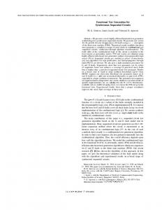
Figure 5: Gate level diagram of a Full Adder The gate-level implementation of the full adder in our library is shown in Figure 5. The precomputed library information for the full adder is summarized in Table 1. The gate-level path < 174 > corresponds to the hierarchical path < l_04_0 >; the notation a_j in a hierarchical path denotes the jfh fanout of line a. The parity of a path denotes the number of inversions along the path. The test vector < UO UO 51 > is a robust test for the falling transition delay fault on the path < 1_1 4_0 >. Similarly, < Ul SO Ul > is a robust delay test for the rising transition delay fault on the path < 1_1 4_0 >. The hierarchical path < a(l) / > in the circuit of Figure 4 corresponds to the hierarchical path < 1_14.0 > in the full adder module. Since the path delay fault on < a(l) / > is a rising path delay fault, we look up the robust test for a rising path delay fault on < 1_1 4_0 > from Table 1. This test vector happens to b e < Ul SO Ul >. Further noting that the parity of the path 1_1 4_0 > is even, we must set 6 to 50 and c to Ul to propagate the rising transition to /. This leads us to the objective (b, 50) and (c, Ul). Similarly, the reader may verify that the objectives (d, SO) and (e, 51) are generated by the path delay fault < /(2) i >< Ul >. Thus the precomputed tests for the path delay fault < a(l) /, Ul > and < /(2) i, Ul >, stored as part of the library information for a full adder leads to the following objectives - (b, 50),
TatVEcun(4.) U0S1U0 U0UQS1
An unsatisfied objective (I, v) is selected from the prioritized objective list, and, to satisfy the objective, an assignment of a value V is attempted to & primary input line I. In order to select / and V, A backward search is made from line / towards the primary inputs of the circuit; when we backtrace from an output line of a module M, we may have more than one input of M which is yet unassigned. We choose the input line of M which is closest to the primary inputs, i.e. whose distance from the primary inputs is minimum, with the belief that it will be easier to satisfy the objective due to its proximity to primary inputs. The value V to be assigned to / is determined from the parity of the path from I to /; if the parity is odd, we set V = v, else we set V = v. The pseudocode for procedure BackJraceQ for the selection of / and V is given in [10]. After value V is assigned to a primary input /, the implications of the assignment are determined. If there is a contradiction between any of the objectives in the objective list and the implications of assignment / = V, the procedure Back-Track of Figure 6 is invoked. When backtracking, / is set to an alternate value, say V, according to the following procedure. ifV £ {51,50}, then V € {51,50}, and, similarly, if V € 171, U0, then V G Ul, UO. If both these asisignments have been Cried previously, then V' = XX. Thus we need not try all four values from the set 51,50, Ul, UQ at each primary input during Back_Track. This reduces the search space from 4" to 2", where n is the number of primary inputs (see [7]). If the number of back tracks made during test generation for a fault / exceeds a predefined limit, we conclude that / is hard-to-test and terminate test generation.
223
procedure BackJTrackQ begin Let L be the set of all lines in the netlist; Let PI be the set of all primary inputs; Let 5 be the stack of all p € PI that have been assigned during procedure backtrace; while (S # NULL) do begin pop entry p from S; if (all alternatives have not been tried at p)then begin make an alternative assignment to p; push p back into S; break; end assign XX to p; carry out the implications of assignment done above; end end
B
N
NM
\X
HL
UL. 26 SO
2
10
4 S 16 32
18 34 66 130
194 386
64
258
770
98
HL
OL 23
HL, 21
17 33
45
41 §1 161
9
64 129 457
89 177 353
32i
705
JSTp GL 21 41 81 161 321 641
Nrp MP 21 41 81 161
321 641
HL
37 105 337
1185 4417 17025
o\6i7 0.022 G.6J4 0.062 6.170 6.&J
(iL
MP
0.021 0.035 0.066 0.166 0.579 2.501
0.054 0.068 0.129 0302 0.983 3.807
Table 2: Path Selection results for n-bit RCA n
4
t
16
32
NT
N M HL,
UL,
HL
UL.
HL
GL
MP
8 16 32 64
14 30
7
13 29 61 125
10
10 22 46 94
10 22 46 94
62 126
15
31
63
22 46 94
16 64 256 1024
B(s) HL
OL
MP
0.013 0.621 6.02? 0.042
0.018 0.022 0.036 0.080
0.041 0.060 0.102
Table 3: Path Selection results for n-bit Parity Checkers
Figure 6: Procedure Back-Track used in MODET
4 Experimental Results MODET was implemented on Sun-SPARC workstations using about 4000 lines of C code. In this section, we report experimental results obtained using MODET to bring out the performance of our tool. Although a number of benchmark circuits are available for delay test generation at gate-level, none are available at module level. We therefore used test circuits of our own, such as ripple carry adders, parity checker trees, comparators, N-to-1 multiplexers, etc. Table 2 shows the results of running our path selection algorithms on an n-bit Ripple Carry Adder (RCA), 2 < n < 64. For both gate-level(GL) and high-level(HL) circuits, we show the number of modules in the netlist, the number of nets, the number of paths selected, and the execution time for running the path selection algorithms. In the table, the number of selected paths are reported for both the selection approaches discussed in Section 2. Results for Approach 1 are given under column MP and for Approach 2 under column HL. We observe that the number of selected paths grows more or less linearly with n, although the total number of paths increases sharply with n. The path selection algorithm (Approach 2) requires more CPU-time on gatelevel circuits. Path selection using Approach 1 was found to be slower than gate-level path selection; this can be attributed to the overheads of flattening the circuit and mapping the gate-level path to a modular path. We can conclude that Approach 2 is superior to Approach 1 in terms of execution time, and the improvement becomes more and more visible with increase in circuit size. In fact, Approach 1 has larger memory requirements during the flattening phase; for a 32-bit parity checker circuit (see Table 3), In the table, NM » NN , Np, and NT are the number of modules, number of nets, the number of selected paths, and the total number of paths respectively. E is the execution time of MODET. Ap-
proach 1 failed due to the large memory requirement. The number of paths selected in the modular circuit was almost identical to that in the gate-level circuit. The savings in execution time become significant for larger values of n. We conducted similar experiments for three other classes of circuits, namely, comparators, multiplexers, and parity checkers. To implement an n-bit comparator, we used a half adder, n — 1 copies of full adders, inverters, 2-input OR and NOR gates. An n-input multiplexer can be constructed using n — 1 2-input multiplexers using a multiplexer tree construction. An n-bit parity checker can be made from 2-bit EXOR gates. The results obtained for all these classes of circuits were similar to those for RCA circuits. Experiments on test generation were performed to compare the time taken and the number of back tracks required for test generation for a module level description as against gate-level. Table 4 shows the results of MODET on an n-bit ripple-carry adder, 2 < n < 64. For each value of n, we show the number of delay path faults, the number of test vectors, the number of faults detected, the number of backtracks, and the test generation time. The fault set for each circuit was obtained by running the hierarchical path selection algorithm of Section 2 (Approach 2), and associating each type of transition, f and |, with every selected path p. The backtrack limit in our experiments was set to 30. With this limit, we did not encounter any case of fault dropping. The number of backtracks in a gate-level delay test generation increases sharply with increase in circuit size. On the other hand, there were no backtracks in running MODET for an RCA composed of full adders as modules. This can be explained by observing that in a module-level RCA, the objectives involve either the primary inputs or the ripple carry lines. When primary inputs are involved as part of an objective, no backtrack or backtrace will be necessary. Even when objectives included ripple carry lines, we found that no backtracks were necessary to satisfy the objectives. We obtained 100% fault coverage for all the circuits. We can conclude from Table 4 that the test generation time is
224
n
#fmHi
2 4 8 16 32 64
42 82 162 322 642 1282
fvecun HL GL 36 38 74 74 144 150 28& 302 576 606 1152
# delected HL UL 42 42 82 82 162 162 322 322 642 642
HL
CJL
4 12 56 240 992
12&2
straction and found that in each case there were large gains in terms of CPU time and memory requirements for hierarchical circuits as compared to their gate-level implementations. Acknowledgements We express our gratitude to Prof. S .M. Reddy of University of Iowa for his constant encouragement and helpful suggestions during this work. Discussions with Ajay Mittal and Gurjeet Saund were very useful.
•renew HL UL 0.044 0.058 0.059 0.104 0.120 0262 0.425 0.902 1.497 4.067
MM
Table 4: Test Generation results for n-bitRCA n 2 4 8 16 32
fffiulu
20 44 92 188
ffvecton HL GL
# detected HL CiL
20 44 92 188
26"
20 44 92 188
44 $2 188
20 44 92 188
ffbictondu HL GL 4 12 28 60
3 12 33 78
nme(i> HL UL 0.032" 0.037 0.038 0.044 0.054 0.075 0.213 d.il9 0.401 0.801
References [1] D. Bhattacharya et al. Test generation for path delay faults using binary decision diagrams. IEEE Trans, on Comp., 44(S):434-441, March 1995. [2] P. Goel. An implicit enumeration algorithm to generate tests for combinational logic circuits. IEEE Trans, on Comp., C-30(3), March 1981.
Table 5: Test Generation results for n-bit Parity Checkers lower when MODET is used on hierarchical netlists. Using the UNIX program profiler, we analyzed that this saving in time was mainly due to faster logic simulation at hierarchical level. There is no entry in Table 4 for a 64-bit gate-level RCA since the test generator fails due to lack of memory. Tables 5 and 6 show the results of MODET for n-bit parity checkers and multiplexer trees respectively. The results are similar to those obtained for a ripple carry adder. In our experimentation on MODET using mux-trees, we observed that there were no backtracks in a gate-level multiplexer; whereas backtracks were necessary for test generation at a hierarchical level. Despite this fact, speedup in test generation was observed since 5-valued logic simulation is much faster for a hierarchical circuit.
5
[3] K. Heragu et al. Statistical methods for delay fault coverage analysis. In Proc. of the 8th VLSI Des. Conf., India, 1995. [4] W.N. Li et al. On path selection in combinational logic circuits. In Proc. of the 25th DAC, pages 142-147, 1988. [5] C J. Lin and S.M. Reddy. On delay fault testing in logic circuits. IEEE Transactions on CAD, CAD6(5):694-703, September 1987. [6] A.K. Majhi et al. An efficient automatic test generation system for path delay faults in combinational circuits. In Proc. of the 8th VLSI Des. Conf, 1995.
Conclusions
[7] S. Patil. An automatic test pattern generator for delay faults in logic circuits. MS thesis, Elec. and Comp. Engg., Univ. of Iowa, May 1987.
We have presented a scheme for the generation of delay tests in circuits described at the module level. This scheme, called MODET, includes software tools for Path Selection and Automatic Test Generation. MODET is also applicable to mixed-level circuits; it considers a path delay fault model at module-level circuits. We have described novel techniques for module-level path selection and test generation. A major feature of MODET which contributes to its impressive performance is the extensive use it makes of library information of the modules handled by it. We have tested our tools on several circuits at various levels of ab-
n 2 4 16 32
# faults 8 20 92 188
# vectan HL (ii. 6 6 16 16 76 76 156 ltt
# detected HL GL 8 8 20 20 92 92 188 188
HL 0
d 36 116
GL 0 0 0
6
[8] S. Patil and S.M. Reddy. A test generation system for path delay faults. In IEEE Trans, on CAD, pages 4043,1989. [9] I. Pomeranz and S.M.Reddy. On testing delay faults in macro-based combinational circuits. In Proc. of the 31st DAC, pages 332-339,1994. [10] C.P. Ravikumar, N. Agrawal, and P. Agarwal. Hierarchical Delay Test Generation Technical Report, Electrical Engineering, IIT Delhi, India, May 1995.
Time(i) HL GL 0.031 0.33 0.036 0.043 0.114 0.143 6.355 0.391
Table 6: Test Generation results for n-bit Multiplexers
225