Jul 28, 2006 - Most existing buffer insertion algorithms, such as van Gin- neken's algorithm, consider only individual nets. As a result, these algorithms tend to ...
18.1
Buffer Insertion in Large Circuits with Constructive Solution Search Techniques Mandar Waghmode, Zhuo Li, Weiping Shi Dept. of Electrical and Computer Engineering Texas A&M University, College Station, TX 77843
ABSTRACT
In real applications, however, the primary objective is to reduce path delay in combinational circuits and reduce the cost of required buffering. Therefore, buffer insertion should be performed at the circuit level rather than at the net level. A simple-minded approach to circuit level buffering is to apply van Ginneken’s algorithm, one net at a time, from primary outputs to primary inputs. Although this approach guarantees that the slacks at the primary inputs are maximized, too many buffers will be inserted since van Ginneken’s algorithm does not control buffer cost. Lillis’ (Q, C, W )-framework, which controls buffering resources, will run into problems due to the reconvergence which are frequently encountered in combinational circuits. Lagrangian relaxation based algorithms for circuit level buffer insertion was proposed in [5, 6]. A restrictive assumption, that buffers are placed equidistant from each other is used in [5]. In practice, however, the availability of space dictates whether a buffer can be inserted in a particular location. The work of [6] tries to get around this restrictive assumption but the resulting algorithms do not scale well. In [5], the CPU time is prohibitively high even without cost optimization. With cost optimizations, their running time is likely to get much worse. A path based buffer insertion algorithm was proposed in [1] that builds on the dynamic programming approaches of [2, 4]. The path based algorithm inserts buffers on statically determined critical paths in the order of their criticality. However, when there are many critical or near critical paths, the order of choosing critical path is problematic and the local optimality it produces may be much different from the global optimality. A network flow based algorithm is suggested in [7]. It tries to identify the nets that should be given priority for inserting buffers by using the min-cut idea in network flow problems. Though this idea is likely to overcome the disadvantages of path based methods, it assumes that buffers are placed to decouple certain parts of the nets irrespective of layout space availability and also assumes that the buffers are placed equidistantly in the interconnect. As mentioned earlier, such a placement may not be feasible and the quality of the solution may deteriorate when the buffer positions are adjusted during the legalization step. In [10, 11, 12], the circuit level buffer insertion problem is coupled with other problems like accurate delay modeling and transistor sizing. In this paper, we propose a new circuit level buffer insertion algorithm called LAB (Look-ahead And Back-off). It uses the dynamic programming based efficient net-level algorithms as its subroutines.
Most existing buffer insertion algorithms, such as van Ginneken’s algorithm, consider only individual nets. As a result, these algorithms tend to over buffer when applied to combinational circuits, since it is difficult to decide how many buffers to insert in each net. Recently, Sze, et al. [1] proposed a path-based algorithm for buffer insertion in combinational circuits. However their algorithm is inefficient for large circuits when there are many critical paths. In this paper, we present a new buffer insertion algorithm for combinational circuits such that the timing requirements are met and the buffer cost is minimized. Our algorithm iteratively inserts buffers in the circuit to improve the circuit delay. The core of this algorithm is simple but effective technique that guides the search for a good buffering solution. Experimental results on ISCAS85 circuits show that our new algorithm on average uses 36% less buffers and runs 3 times faster than Sze’s algorithm. Categories and Subject Descriptors: B.7.2 [Integrated Circuits]: Design Aids - Placement and routing J.6 [Computer-aided Engineering]: Computer-aided Design General Terms: Algorithms, Performance, Design Keywords: Buffer Insertion, Cost optimization, Physical Design, Interconnect synthesis
1.
INTRODUCTION
Buffer insertion is an effective technique for reducing interconnect delay. For a single net, van Ginneken [2] proposed a dynamic programming algorithm to maximize the slack, without considering buffer cost. As the cost of required buffering resources to meet the timing constraints is exploding [3], minimizing buffer cost has become paramount. Lillis et al. [4] extended van Ginneken’s algorithm to minimize the buffer cost while satisfying the timing requirements. A great amount of research has been done for buffer insertion of single nets.
Permission to make digital or hard copies of all or part of this work for personal or classroom use is granted without fee provided that copies are not made or distributed for profit or commercial advantage and that copies bear this notice and the full citation on the first page. To copy otherwise, to republish, to post on servers or to redistribute to lists, requires prior specific permission and/or a fee. DAC 2006, July 24–28, 2006, San Francisco, California, USA. Copyright 2006 ACM 1-59593-381-6/06/0007 ...$5.00.
296
The rest of the paper is organized as follows. Section 2 presents the problem statement. Section 3 explains the main idea of the look-ahead and back-off strategies of the algorithm. Section 3 presents the overall flow of the algorithm. Section 5 describes the methods to further speedup the algorithm. The experimental results for LAB algorithm are presented in Section 6.
2.
each edge e connecting a gate input to a gate output is associated with constant delay D(e), each gate input node v is associated with input capacitance C(v) and each gate output node v is associated with driving resistance R(v). Following previous researchers [2, 4], the Elmore delay model is used for interconnect and a linear delay model is used for gates and buffers. For each edge e = (vi , vj ), signals travel from vi ”to vj . The Elmore delay of e is D(e) = “ R(e) C(e) + C(vj ) , where C(vj ) is the downstream capac2 itance at vj . For any gate or buffer b at vertex vj , the gate or buffer delay is D(vj ) = K(b) + R(b) · C(vj ), where C(vj ) is the downstream capacitance at vj . For a gate input node v, the capacitance viewed from upstream is C(v). Similarly, the capacitance viewed from upstream for inserted buffer b is C(b). For any subgraph G0 = (V 0 , E 0 ) of G, a candidate buffer assignment is a function α(G0 ) that specifies for each possible buffer position in G0 whether there is a buffer and if so, the type of buffer. We call α a candidate because it is a candidate for the optimal one. W (α(G0 )) denotes the total buffer cost of α(G0 ). If a directed path exists from node u to node v in G0 , then delay of the path from u to v under assignment α is defined as X D(u, v, α) = (D(vj ) + D(e)),
PROBLEM DESCRIPTION
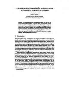
We represent a combinational circuit as a Directed Acyclic Graph (DAG) G = (V, E). The set of nodes V = Vt ∪ Vn , where Vt are primary input, primary output, gate input and gate output nodes in the circuit, and Vn are internal nodes and possible buffer positions in the interconnect routing trees. The set of edges E consists of the edges in the interconnect routing trees and input-to-output edges connecting the input and output nodes in the gates. Fig. 1 shows an example combinational circuit and the corresponding DAG representation. Primary Inputs b d c
a
a
c
b
d e
e
f
f h i
g
j
n
m
p
q
l
k o
r
s
u t v w primary outputs (a)
g
n
m
p
q
l
k
j
h i
e=(vj ,vk )
o r
where the sum is over all edges e in the path from u to v. The Required Arrival Time (RAT) Q(u) at node u in G0 is a user-specified value if u is a primary output node. Otherwise, RAT at node u under α is defined as follows.
s
t
u
v
w
Q(u, α) =
min {Q(v) − D(u, v, α)}
v∈O(G0 )
Also, the Arrival Time (AT) T (u) at a node u is a user specified value if u is a primary input node. Otherwise, AT at node u under α is defined as follows.
(b)
Figure 1: Example combinational circuit (a) and its corresponding DAG representation (b).
T (u, α) = max0 {T (v) + D(v, u, α)} v∈I(G )
The Slack at a node u under α is defined as follows. Since our algorithm starts with sub-circuits and gradually expand to the entire circuit, we use subgraphs to represent the corresponding sub-circuits. For any subgraph G0 = (V 0 , E 0 ) of G, the set of input nodes I(G0 ) consists of all nodes in V 0 with no incoming edge in E 0 , and the set of output nodes O(G0 ) consist of all nodes in V 0 with no outgoing edge in O(G0 ). Following this definition, I(G) is a set of all primary inputs and O(G) is a set of all primary outputs of the circuit. In the buffer insertion problem, a buffer library B is provided as a part of the problem statement. The locations where buffers can be inserted are given as a function f : Vn → 2B . Under this definition, each node in the interconnect routing tree allows certain types of buffers, or no buffer. Each buffer type Bi ∈ B is modeled by driving resistance R(Bi ), input capacitance C(Bi ), intrinsic delay K(Bi ) and cost W (Bi ). The cost of a buffer can be either area or power or any other criteria, depending on the optimization objective. Each interconnect edge e is modeled as a π type RC circuit and is associated with resistance R(e) and capacitance C(e). Each gate is modeled in a similar manner as a buffer. Thus
S(u, α) = T (u, α) − Q(u, α) Also, the slack of subcircuit G0 under α is given as S(α) = min0 S(v, α) v∈I(G )
The optimal solution to this problem is a buffer assignment α for G that has minimum cost among all the assignments, and S(α) is greater than or equal to a given target slack value.
3. LOOK-AHEAD AND BACK-OFF As shown in Figure 2, suppose we have added a certain amount of buffers already in the circuit, and the resulting circuit slack is S. If we add one more buffer in position a, the circuit slack becomes Sa . Alternatively, if we add a buffer in position b, the circuit slack becomes Sb . Furthermore, let Sb be worse than Sa . But if we choose to insert buffer at a and then to insert one more buffer elsewhere in the circuit, the average slack improvement is much lower compared to the case where we would have chosen to insert buffer at b. Thus, if we just ”look-ahead” one level, we can make a better
297
Algorithm 1 Look-ahead to insert one buffer. 1: Let α(G) be the current buffer assignment. 2: for each net ηi ∈ G do 3: Insert one more buffer into ηi 4: Cumulative slack improvement si = 0 5: for each net ηj ∈ G do 6: Insert one more buffer into ηj 7: Compute slack improvements of G due to the two buffers. 8: si = si + slack improvements 9: end for 10: end for 11: Insert a buffer into net ηi with maximum si
Better Slack Avg. on adding one more buffer after a S_a
Avg. on adding one more bufer after b
S_b
S
Figure 2: Look-ahead strategy for buffer insertion.
decision about which buffer should be inserted. For the sake of simplicity, assume we have only one buffer type for now. Then, the look-ahead level is simply the number of additional buffers we try while evaluating the future effectiveness of inserting a buffer in a particular location. Similarly, taking out a buffer from the circuit that causes the least slack worsening on removal is called “back-off” in our algorithm. Look-ahead combined with back-off provides not only an effective solution search strategy but also a very flexible algorithm in terms of cost reduction and run-time trade-off. In a nutshell, LAB is a guided solution search. It starts from a state where no or a few buffers may have been inserted in the circuit. It goes on inserting buffers step by step using the look-ahead technique. In between the insertion steps, by using back-off technique, it reverts some of the past insertion decisions that prove less effective later on. Along with the central ideas of look-ahead and back-off, the techniques used to speed-up the operation play an equally important role in the algorithm.
positions chosen under a lower cost non-redundant assignment may not prove to be good choices for a higher cost assignment. Also, RAT at the nodes in the circuit keeps changing as we go on inserting or removing buffers in the circuit. Hence, we just specify the cost of buffers inserted in each net under an assignment rather than the exact buffer positions in the net. As noted in Section 3.1, given RAT at the leaf nodes of a net, for each cost value, there is a unique non-redundant assignment found with Lillis’ algorithm. Thus, the buffer positions are implicitly specified when cost of buffers inserted in each net under an assignment is specified. We can also look ahead two steps, by having one more nested loops. For a simple case of only one buffer type, the time complexity of Algorithm 1 to insert each buffer is O(n2 ), where n is the size of the circuit. If we look ahead two steps, then the time complexity will be O(n3 ).
3.1 Definitions
3.3 Back-off
Given any net η and the RAT at each leaf node, a candidate buffer assignment for η can be expressed by (Q, W ), where Q is the RAT and W is the cost. Since η has a driving gate, the traditional capacitance C is not needed. A candidate (Qi , Wi ) of η is called non-redundant if there is no other candidate of η that has greater RAT than Qi and lower cost than Wi . We denote by N (η) the set of all nonredundant candidate for η. Note that there is at most one non-redundant candidate for each possible value of W . Lillis’ algorithm [4] along with predictive pruning [9] is a core subroutine used in LAB for computing N (η). Let α(G) be a candidate assignment of the whole circuit G. For any net ηi , let N (ηi ) be the set of non-redundant candidates of ηi when RAT Q(v) = Q(v, α(G)) at each sink v of ηi .
Similar to the look-ahead strategy, we can look back to decide which buffer is least effective and to remove it. The idea here is to let the look-ahead do the job of careful selection, and back-off sometimes to correct the decisions taken by look-ahead which proved less effective in retrospect. Therefore we need a faster back-off routine which need not be as careful as look-ahead while removing buffers. Back-off complements look-ahead in the sense that wrong choices made by look-ahead can be corrected with back-off, and consequently, insertion can be more aggressive and faster. The back-off subroutine is as follows. Algorithm 2 Back-off to delete a buffer. 1: Let α(G) be the current buffer assignment. 2: for each net ηi ∈ G do 3: Delete one buffer from ηi 4: Compute slack increase with the buffer removed. 5: Restore the buffer to ηi 6: end for 7: Delete the buffer with least slack increase.
3.2 Look-ahead Now we show how to find where to insert the next buffer, by looking ahead one step in Algorithm 1 . For simplicity, we depict the case of only one buffer size. When more buffer sizes are available, an insertion move can either be inserting an additional buffer or switching to a higher size so as to increment the cost of buffers inserted in a perticular net. Note that when we decide the next assignment after a look-ahead step, we are only incrementing the number of buffers or the cost of buffers inserted in the selected net. But we do not fix the new buffer positions. This is because optimal placement of buffers for a net may be drastically different at different buffer costs. In other words, buffer
Similar to Algorithm 1, we do not fix any buffer positions while deciding the assignment after back-off but just decrease the cost or number of buffers in a particular net. The back-off technique adds a great amount of flexibility and effectiveness to the overall buffer insertion algorithm. It not only improves the cost performance of the algorithm but also the run-time of the algorithm. With back-off correcting
298
wrong choices made while inserting buffers, we can cut back on the number of look-ahead levels resulting in a much faster algorithm. In fact, a fast greedy net-based insertion without any look-ahead can be employed to insert buffers in the beginning. Look-ahead technique is used only in the later stage of the algorithm when it becomes necessary to make careful insertion decisions. This combination of techniques gives us a flexible framework that can be used to trade off the solution cost and run-time performance.
net are independent of the RAT at its sink. Therefore, nonredundant candidates for a 2-pin net can be computed in the preprocessing step even before the start of the algorithm. Thus, most of the CPU time in one circuit slack computation is spent in processing multi-pin nets with (Q, C, W ) framework. Therefore to further speed-up this scheme,we need to reduce the number of circuit slack computations and more specifically the number of non-redundant candidate computations on multi-pin nets.
4.
5.1 Fast and Greedy Net-based Buffer Insertion
OVERALL FLOW
Algorithm 3 shows the overall flow of the algorithm that brings together various strategies discussed till now. The details of the greedy net-based insertion are provided in the subsequent section.
Greedy net-based insertion combined with back-off enables us to quickly get to a point where look-ahead becomes necessary to make careful insertion decisions. A routine employed for this purpose is sketched in Algorithm 4. Note that this sketch is just an example way of quickly identifying the buffers that are obviously effective and do not require lookahead to identify them. The greedy insertion based on local improvements could be implemented in some other manner as well.
Algorithm 3 Top-level view of the algorithm. 1: Input parameters: St = Target Slack, l = Look-ahead level, f = Fraction of buffer cost to remove in back-off. 2: Generate α(G) with net-based insertion followed by back-off such that S(α(G)) ≥ St . 3: Cost of added buffers Wa = W (α(G)) 4: while (f ×Wa ) ≥ minimum possible cost decrement do 5: Cost of removed buffers Wr = 0 6: while Wr < (f × Wa ) do 7: Remove buffers from α(G) with back-off and update Wr . 8: end while 9: Wa = 0 10: while S(α(G)) ≤ St do 11: Insert buffers in α(G) with look-ahead and update Wa . 12: end while 13: end while 14: return α(G).
Algorithm 4 Fast net-based insertion followed by back-off. 1: Let α(G) be current assignment and St be desired circuit slack. 2: while S(α(G)) < St do 3: find set of critical nets R 4: for Each critical net η ∈ R do 5: Find improvement in AT at the root of n, L(η), if one more buffer is inserted in η 6: end for 7: Sort the nets in R in the decreasing order of L(η) 8: Desired cumulative improvement I 0 = (St − S(α(G))) 9: Cumulative improvement I = 0 10: for each net η in sorted order do 11: Insert a buffer in η to increment W (α(G)) 12: I = I + L(η) 13: if (I ≥ I 0 ) then break the for loop 14: end for 15: Update the circuit slack. 16: end while 17: while S(α(G)) ≥ St do 18: Decrement α(G) with back-off. 19: end while
As seen in Algorithm 3, trade-offs can be made in the performance of the algorithm with two input parameters namely look-ahead level l and fraction of added buffer cost that should be removed in back-off f . In our experiments with ISCAS85 benchmark circuits, looking ahead just by one level and removing about 20% of the added buffers with back-off yielded tremendous improvements in cost with very efficient run-times. There was no improvement or marginal improvement with higher look-ahead levels and back-off fractions. Thus, referring to Algorithm 3, we recommend l = 1 and f = 0.2 which provides efficient run-time without losing the quality of results of cost optimization.
5.
In the greedy net-based insertion, we avoid frequent circuit slack computations and look at the Arrival Time improvement at the root of a net as a measure of effectiveness of a buffer insertion move. We determine the critical nets in the circuit and populate the critical nets greedily with buffers till a particular slack requirement is achieved. Performing this greedy buffer insertion only on the critical nets prevents it from adding a lot of unnecessary buffers. Back-off is invoked after such greedy insertion to get rid of redundant buffers. The use of this greedy insertion is as shown in the top level Algorithm 3.
SPEED-UP TECHNIQUES
From Algorithms 1 and 2, we can see that the most computationally intensive task is that of finding circuit slack while evaluating the effectiveness of the possible moves. To be more specific, an assignment specifies the cost of buffers to be inserted in each net. The circuit slack is then computed by processing the nets in their topologically sorted order with Lillis’ (Q, C, W ) framework [4, 9]. However, looking closely at a single circuit slack computation, we can see that non-redundant assignments for a 2-pin
5.2 Reducing The Number of Buffer Positions Evaluated Clearly in Algorithm 1, if net ηi is not critical, then inserting a buffer to ηi will not achieve maximum slack improvement. Therefore, we need to determine the critical nets under assignment α in order to reduce the number of nets
299
considered. The critical nets are determined after every insertion move. With each new buffer added in the circuit, the nets that were previously critical may become non-critical and vice versa. Also, the data generated in one look-ahead iteration can be used to perform more than one buffer insertion moves i.e. rather than just inserting one buffer in each iteration, we continue adding the second best increment, third best and so on as long as the buffers are being added on critical nets because the back-off iterations will correct these moves in case they later prove to be less effective.
section do not include this technique; we intend to implement this as a future work.
5.5 Faster Identification of Some Back-off Moves Let α(G) be the current assignment of the whole circuit graph and α(η) = α(G ∩ η) represent the partial buffer assignment in net η under α(G). Let node u be the root or source node of η. Also, let α0 (η) be the non-redundant assignment having next lower cost than W (α(η)). Consider a condition such that: S(u, α(G)) ≥ (S(α(η)) − S(α0 (η)))
5.3 Reducing Number of Multi-pin Nets Processed in One iteration
If this condition is true for some net η ∈ G, then it can be easily seen that there is enough surplus slack at node u such that decrementing α(G) over η will not change the circuit slack. Thus, the decision of adding the last buffer in η had no effect on the circuit slack and hence η can be safely chosen for back-off. Note that the effort of computing circuit slack for all possible back-off moves and then choosing the best move is saved by identifying the back-off moves with above criterion. This is used in all the back-off stages of the algorithm. Also, applying this criterion more aggressively, i.e. choosing nets for back-off that are likely to have little if any effect on the circuit slack based on such a local comparison, can yield additional speedup.
Since we add or remove buffers one at a time, previously computed RAT information can be reused. Thus, if we change the number of buffers inserted in a particular net, then the RAT needs to be updated only for the nodes in the fan-in cone of the net in question. Moreover, we can approximate the slack wherever exact slack is not needed. More specifically, after a buffer is added or removed from a net η, referring to Figure 3, the algorithm processes only the most critical path in the fan-in cone of η to get the new approximate value of circuit slack. This way, significantly fewer nets are processed to get circuit slack. Most critical Primary Input
6. EXPERIMENTAL RESULTS OF LAB ALGORITHM
Fan in cone
Table 1: Size of the benchmark circuits. Circuits # of source # of sink # of buffer nodes nodes positions c432 196 343 868 c499 243 440 1216 c880 443 775 1632 c1355 587 1096 1868 c1908 913 1523 4037 c2670 1502 2292 7192 c3540 1719 2961 7729 c5315 2485 4509 11403 c6288 2448 4832 10865 c7552 3720 6253 16758
Net whose cost has changed
Figure 3: Estimating circuit slack approximately. This approximate computation is used during the backoff stages of the algorithm. Also, if l is the look-ahead level, then the circuit slack of the assignment found by adding l th additional buffer is needed only for estimation purposes, and hence is approximately computed.
The newly proposed Look-ahead and Back-off (LAB) algorithm is compared with a recently proposed path based buffer insertion (PBBI) algorithm of [1]. Since the algorithms of [5, 7] assume that the buffers can be placed anywhere on the interconnect, they can not be compared directly with our algorithm. Table 1 shows the ISCAS85 benchmark circuits and their respective sizes in terms of number of source and sink nodes. The interconnect lengths, resistance and capacitance data for the test-cases is generated by scaling the layouts of these circuits performed in 0.18µ technology to create the need for buffering. Only one buffer type is used for these experiments. Timing constraints i.e. the RAT at the primary output nodes is determined by first computing the maximum achievable slack with given legal buffer positions. Table 2 shows the comparison of LAB and PBBI [1] algorithm with
5.4 Temporarily Partitioning The Multi-pin Nets If the given circuit has larger nets with many buffer positions, then such interconnect trees can be partitioned by fixing a buffer temporarily in a legal position that partitions the tree proportionately. Such a partitioning creates smaller multi-pin nets that can be processed more efficiently further reducing the effort of circuit slack computations. Such restrictions can be placed in the early stages of the algorithm and removed in later stages in order to achieve better quality. The current exprimental results presented in the next
300
Table 2: Comparison against path-based algorithm ([1]). PBBI [1] LAB (New) # of buffers Time(s) # of buffers Time(s) Reduction Speed up c432 61 0.4 37 1.5 39.3% 0.26x c499 69 0.7 47 1.2 31.8% 0.58x c880 48 1.9 29 0.7 39.5% 2.71x c1355 143 3.9 78 3.6 45.4% 1.08x c1908 137 16.9 96 7.6 29.9% 2.22x c2670 187 63.2 94 10 49.7% 6.32x c3540 202 85.2 109 21.6 46% 3.94x c5315 269 194.4 164 21 39% 9.25x c6288 508 182 433 149 14.91% 1.22x c7552 282 429.4 208 49.5 26.2% 8.67x Average 36.2% 3x Circuits
respect to number of buffers inserted and the CPU time. PBBI and LAB are run for the same input circuit and on the same machine with a 1.5GHz Pentium M processor and 512MB RAM. Referring to Algorithm 3, the experimental results are obtained with l = 1 and p = 0.8 for LAB. On an average, LAB gives 36% reduction in number of buffers inserted and 3× speed-up as compared to PBBI.
7.
[3] P. Saxena, N. Menezes, P. Cocchini, and D. A. Kirkpatrick, “Repeater scaling and its impact on CAD,” IEEE Trans. on CAD, 23(4):451–463,April 2004. [4] J. Lillis, C. K. Cheng and T.-T. Y. Lin, “Optimal wire sizing and buffer insertion for low power and a generalized delay model,” IEEE Trans. Solid-State Circuits, 31(3), 437–447, 1996. [5] I-Min Liu, A. Aziz, D.F. Wong and H. Zhou, “An efficient buffer insertion algorithm for large networks based on Lagrangian relaxation,” ICCD 1999, 210–215. [6] I.-M. Liu, A. Aziz, and D. F. Wong, “Meeting delay constraints in DSM by minimal repeater insertion,” Proc. of DATE, 436–441, 2000. [7] R. Chen and H. Zhou, “Efficient Algorithms for Buffer Insertion in General Circuits Based on Network Flow,” ICCAD 2005, 509–514. [8] C. J. Alpert and A. Devgan. “Wire segmenting for improved buffer insertion,” Proc. 1997 DAC, 588–593. [9] W. Shi, Z. Li and C.J. Alpert, “Complexity analysis and speedup techniques for optimal buffer insertion with minimum cost,” Proc. 2004 ASPDAC, 609–614. [10] Y. Zhang, Q. Zhou, X. Hong and Y. Cai, “Path-based timing optimization by buffer insertion with accurate delay model”, Proc. 5th International Conference on ASIC, Vol.1:89–92, Oct. 2003. [11] Y. Jiang, S. Sapatnekar, C. Bamji and J. Kim, “Interleaving buffer insertion and transistor sizing into a single optimization”, IEEE Transactions on VLSI Systems, 6(4):625–633, Dec. 1998. [12] K.S.Lowe and P.G. Gulak, “A joint gate sizing and buffer insertion method for optimizing delay and power in CMOS and BiCMOS combinational logic”, IEEE Trans. on CAD, 17(5):419–434,May 1998.
CONCLUSIONS
We presented a buffer insertion algorithm that optimizes buffer cost for the whole circuit while trying to meet the timing constraints. As compared to earlier approaches, our approach has a more global view and predicts a better buffer distribution for the whole circuit. The main strength and contribution of our algorithm is this better cost saving ability and it is evident from the consistent cost savings seen in the experimental results. This also makes it useful as a precursor to any other buffer insertion scheme that can take advantage of the cost distribution predicted by our framework. Main limitation of this framework is that it is not an exact algorithm like [2, 4] in the sense that it has tuning parameters that balance its runtime and quality of results and the speed-up techniques also play an important role in the run-time improvement. Driver or gate sizing is a natural extension for a circuit level buffer insertion algorithm and adapting this framework for simultaneous driver sizing is the future direction of this work. Gate sizing can be accomodated in our framework by treating gates just like buffers and extending the concept of a net to that of a composite net made up of the gate’s input and output nets.
8.
REFERENCES
[1] C. Sze, C. Alpert, J. Hu and W. Shi, “Path-based buffer insertion,” Proc. 2005 DAC, 509–514. [2] L. P. P. P. van Ginneken, “Buffer placement in distributed RC-tree network for minimal Elmore delay,” Proc. 1990 ISCAS, 865–868.
301