2014 Fifth International Symposium on Electronic System Design
CA Based Scalable Protocol Processor for Chip Multiprocessors Mamata Dalui
Biplab K Sikdar
Department of Computer Science and Engineering National Institute of Technology Durgapur, West Bengal, India 713209
[email protected]
Department of Computer Science and Technology Indian Institute of Engineering Science and Technology Shibpur, West Bengal, India 711103
[email protected]
Tag
Index
Tag
Status bits
Data
Tag
Status bits Data
Bus R/W
Memory address
Invalidation broadcast
Bus
Abstract—The protocol processor (PP) is a key component of the cache coherence controller (CC) in a Chip Multiprocessors (CMPs) cache system. PP computes the state of a block on every transaction (read/write operation) on the block while maintaining cache coherence in CMPs. This work proposes a novel design approach for the PP which can cater to the pressing need for determining the state of a data block with high accuracy. It is developed around the modelling tool of cellular automata (CA) invented by von Neumann in 1950’s. The inherent regular, modular, cascadable structure of CA ensures high scalability and robustness in exascale design solutions. Index Terms—CMPs, cache coherence, coherence controller, protocol processor, cellular automata
Offset
PP
CPU R/W
CC
Present state =
= Hit/Miss
Next state of the block
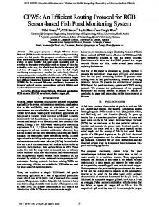
I. I NTRODUCTION Fig. 1.
The cache coherence controller (CC) is the key hardware component responsible for maintaining the coherency of shared data in Chip Multiprocessors (CMPs) [1] [3] [5]. The heart of CC is the Protocol Processor (PP) [4] which computes the states of a block in caches on every cache read/write operation. The conventional design of PP is capable of ensuring accurate operation. However, it may be perceptive to several faults in hardware e.g. stuck-at faults. An insignificant defect in the hardware logic of PP can introduce major inconsistencies in cache line state computation [5]. For example, if a cache line state is computed as ‘shared’ (S) instead of ‘modified’ (M), it denies the issuance of invalidation message and may cause a serious damage to the system performance as well as its reliability. On the other hand, setting of an ‘M’ state instead of ‘S’ results in unnecessary write back and message exchange. It causes a huge power loss in CMPs. This scenario motivates us to introduce radical change in the design approach of PP. The modelling tool of cellular automata (CA) [6], invented by von Neumann in 1950’s is considered for the design. The CA have been successfully employed to design the verification unit (VU) for cache coherence controller in [8]. In this work, a CA based model of Protocol Processor which can cater to the pressing need for determining the state of a block with high accuracy is reported. The proposed CA based PP can also work as an individual component running parallelly with the VU. In a design with conventional PP and VU, the CA based PP provides the computed cache states when the VU identifies inconsistencies. 978-1-4799-6965-4/14 $31.00 © 2014 IEEE DOI 10.1109/ISED.2014.40
Baseline architecture of a CC as in [5]
II. OVERVIEW OF THE P ROPOSED D ESIGN The baseline CC architecture considered for the current design is shown in Fig. 1. It consists of queues for data and coherence transactions, and a Protocol Processor (PP) [2]. The PP essentially is an FSM. It computes the next state of a cache line, containing a block B, on a read/write operation by bus or CPU. An apparently insignificant incorrect decision of PP can introduce serious inconsistencies in the cache states. On the other hand, frequent updation of cache states against each read/write operation in processor cores demand high speed decision taking capability of a PP. Specially, in CMPs with thousands of processor cores such an issue poses a grave concern to the designers. In this work, we have realized a CA based scalable architecture of PP that can perform high speed computation of cache line states at each read/write operation. The target is to allow the CA based PP also to run parallelly with the VU [5], [8] in a system with conventional PP and the VU, and when the VU identifies inconsistencies in cache line states, then the states computed in CA based PP can provide the correct cache line states. The position of the proposed CA based PP is indicated in Fig. 1 (reproduced from [5]). For ease of understanding, in this paper we illustrate design of CA based PP realizing MSI protocol. In MSI, each of the following cases indicates that the cache line states of a block B at time t are coherent, when 161
IN
OUT
IN
Cell 1 (FF)
OUT Cell i−1 (FF)
IN
OUT
IN
Cell i (FF) NSi
f1
Xi−1
OUT
Cell i+1 (FF)
capable of portraying the behavior of the PP. That is, if the present state of the CA embodies the present states of a block B in L1 caches, then based on the inputs e.g. read/write by bus or processor, the CA cells will be configured with suitable rules. The CA dynamics as it is striding over time, the next states of the CA cells conform with the next states of the block B in the caches. For ensuring a quick decision on the cache line states, the steps (t) of CA runs should be minimum, ideally (t=)1.
IN OUT Cell n (FF)
Xi fi
fn
Xi+1
fi: combinational logic null boundary
Rule 192: NSi = Xi−1 Xi
Fig. 2.
Rule 207: NSi = X’i−1 +Xi
null boundary
An n-cell null boundary CA
-
P0
P1
P2
P3
I
I
I
I
Initial state of Block B (all Cis’ copies are I)
Transaction
Case 1: Block B in all the caches (Cs) are in I (invalid) Case 2: B in all the caches (Cs) are in S (shared) Case 3: B in some Cs are in I and others are in S Case 4: B in one cache is in M (modified) and in all others are in I. That is, a PP for MSI protocol should properly satisfy the four cases (case 1 to 4) as well as should follow the state transitions as of MSI. For an n processor core CMPs having their private L1 caches C1 , C2 , ..., C𝑛 , 2-bit status code is considered for the states I(‘00’), ‘S’(10), and ‘M’(11). 15 7
0
0
0
0
0
0
0
0
1. read by Po
29
64
12
4
12
4
12
4
CA representing Initial state of Block B CA rule is set and run 1 step
1
0
0
0
0
0
0
0
Next state of block B
2. read by P1
12
4
29
64
12
4
12
4
CA rule is set and run 1 step
1
0
1
0
0
0
0
0
Next state of block B
3. write by P1
2
4
29
115
2
4
2
4
CA rule is set and run 1 step
0
0
1
1
0
0
0
0
Next state of block B
4. read by P3
12
4
12
4
12
4
29
64 CA rule is set and run 1 step
0
0
1
0
0
0
1
0
Next state of block B
14 Fig. 4.
12
13
3
11 6
4
1
8
Fig. 3.
0
The states (represented by 2-bit status code) of a block B in all the n caches collectively fed as initial seed for the 2n-cell CA. Before the very first reference to block B, the cache line states of block B are ‘I’ in all the caches - that is, an all 0s seed. Whether the current transaction is read or write (read is represented by ‘0’ and write by ‘1’) and the transaction if requested by bus then ‘0’ and if by processor, then ‘1’ are considered to select the CA cell rules. Once all the CA cells are configured with appropriate rules, the CA is run for 1-step. The next state generated is then used to update the cache states of the cache lines for block B. On every such transaction, the cache line states are fed as the seed for the CA and based on the current inputs i.e. read/write by bus or processor, the CA cell rules are configured. The following example illustrates the functioning of the PP. For ease of understanding, let us consider a system of 4 caches C1 , C2 , C3 & C4 and operations on a block B. Initially, none of the caches have a copy of block B i.e. the collection of cache states for B is ‘I’s (Fig. 4). Now, P0 issues a read request for B. With this read operation, the state of cache line for B in C0 is ‘S’ and in other caches are ‘I’. The status vector is, therefore, 10 00 00 00 (Fig.4). The next transaction is a read by P1 . So, now block B in C0 and C1 are in ‘S’ state and other caches are in ‘I’ state (represented as 10 10 00 00). The third transaction being a write operation by P1 , P1 ’s cache line only will hold the block in ‘M’ state and the cache lines in other
2
9 10
Functioning of PP
5
State transition diagram of SACA
The 𝑛-cell cellular automaton (𝐶𝐴), an autonomous finite state machine (Fig. 2), evolves with time and its state transition diagram consists of cyclic and non-cyclic states (Fig. 3, ‘0’ is the cyclic state, called attractor [6]). The combination of present states of a CA-cell is the Min Term of a 3-variable 𝑡 𝑡 , 𝑆𝑖𝑡 , 𝑆𝑖+1 switching function and is referred to as the Rule 𝑆𝑖−1 Min Term (RMT). The 4-cell null-boundary 3-neighborhood (2-state per cell) CA of Fig. 3 is a uniform SACA (single length cycle single attractor CA). Its states lead to an attractor (state ‘0’) of single length cycle. The next state logic (𝑓𝑖 ) of each CA cell follows NS𝑖 = x𝑖−1 .x𝑖 (defined as rule 192). The CA based design of PP employs a 2n-cell CA for a system of n processor cores (also n number of L1 caches). The stringent requirement is that the global dynamics of a CA state space as it evolves in successive time steps, should be
162
TABLE I L IST OF CANDIDATE RULES FOR THE CA BASED PP Operations Processor read
CA-cell rule R𝑖0
111 d
110 d
101 d
RMTs 100 011 1 1
Bus read
R𝑖1 R𝑗0
d d
1 d
0 d
0 0
Processor write
R𝑗1 R𝑖0
d d
0 d
0 d
Bus write
R𝑖1 R𝑗0
d d
1 d
R𝑗1
d
0
Rules 010 1
001 d
000 1
d 1
d 1
0 d
0 0
0 1
d 1
d 1
0 d
0 1
0 d
0 0
d 1
d 1
0 d
0 0
0
0
d
d
0
0
processors are in ‘I’ state (00 11 00 00). The last transaction is a read by P3 . So, both P1 and P3 ’s copy will be in ‘S’ and other cache copies of B are in ‘I’ state (00 10 00 10).
29,31,61,63,93,95,125,127, 157,159,189,191,221,223,253,255 64,68,72,76,192,196,200,204 12,14,44,46,76,78,108,110 140,142,172,174,204,206,236,238 0,4,8,12,128,132,136,140 29,31,61,63,93,95,125,127, 157,159,189,191,221,223,253,255 115,119,123,127,243,247,251,255 0,2,32,34,64,66,96,98, 128,130,160,162,192,194,224,226 0,4,8,12,128,132,136,140
Table I. The hardware realization of the PP with one set of rules chosen from Table I, is shown in Fig. 6. As mentioned earlier, for a system of n-caches, we have employed a 2n-cell CA. The transaction code along with the code for transaction by bus or processor for i𝑡ℎ processor are used to set the rules 𝑡ℎ for 𝑖𝑡ℎ 0 and 𝑖1 CA-cells. For a write operation by processor P𝑖 , we select the following rule combinations - R𝑖0 = 29, R𝑖1 = 115, R𝑗0 = 2 and R𝑗1 = 4, where R𝑖0 & R𝑖1 correspond to processor P𝑖 and R𝑗0 & R𝑗1 correspond to a processor P𝑗 other than P𝑖 . Similarly, for a read operation by processor P𝑖 , the set of rules selected are the - R𝑖0 = 29, R𝑖1 = 64, R𝑗0 = 12 and R𝑗1 = 4. The 4-to-1 multiplexer is used to decide on the CA rules for a cell. The transaction code (‘0’ for read and ‘1’ for write) and the code for transaction by bus or processor (‘0’ for bus and ‘1’ for processor) are used as the select inputs for the MUX. The state transition of the CA of Fig. 5 realizes the state transition of MSI protocol. For a system of two processors P𝑖 & P𝑗 , the state change of P𝑖 is described in Fig. 5(e). Initially, P𝑖 encounters a read miss for a block B and the state of cache line for B is changed from ‘I’ to ‘S’ (denoted by 1000/1010 in Fig. 5(e)). A signal is then sent to P𝑗 , the other sharers, if any. With a read hit, P𝑖 ’s cache line remains in ‘S’. For a write hit by P𝑖 for block B, P𝑖 can change state to ‘M’ (denoted by 1100 in Fig. 5(e)). When P𝑖 is in ‘M’ state, a read or write hit for B, there is no change in P𝑖 ’s cache line state. At this state, if there is a P𝑗 write miss, P𝑖 ’s cache line state changes to ‘I’ (denoted by 0011 in Fig. 5(e)). For P𝑗 read miss, the state of P𝑖 ’s cache line for B is set to ‘S’. The hardware realization of the CA based PP is shown in Fig. 6. This can fully simulate the behavior of PP realizing the MSI protocol.
III. CA RULE S ELECTION Exhaustive analysis of the various local perturbations to each CA cell that stimulates the emergent behavior and computational capacity of a PP has come up with a wide variety of candidate rules for the different cells of the CA. Each CA rule is defined by its corresponding next state function which is a 3-variable boolean function. Hence, selecting a CA cell rule is merely deciding the boolean logic function. Since for the CA based design of PP, based on the present state and other inputs, only a few number of RMTs are involved in next state computation of a CA cell (corresponding to a signal line) and various different CA rules can have the same set of outputs for the same set of RMTs, for each CA cell, we can obtain many possible rules. Table I delineates all the possible rules for each of the CA cells corresponding to a signal line. For example, for a read operation by processor P𝑖 , the i𝑡ℎ 0 CA cell (corresponding to R𝑖0 signal line changes state only on RMTs 0(000), 2(010), 3(011), and 4(100) and the other RMTs are don’t cares. The desired next state corresponding to the RMTs 0, 2, 3 and 4 should be 1. So, there can be more than one possible CA rules for which RMTs 0, 2, 3 and 4 are 1. Based on this logic we have found all the possible rules for the CA cells. The 1𝑠𝑡 row of Table I lists the CA rules for a processor read by processor P𝑖 . The rules R𝑖0 & R𝑖1 are destined for the 𝑡ℎ i𝑡ℎ 0 & i1 CA cells. Columns 3-10 list the required 8 RMTs that determine the rules. An entry ‘d’ in column 3 of the 1𝑠𝑡 row indicates the next state for the RMT 111 is don’t care (it can be either 0 or 1) for the design. For designing the PP, any rule listed in Table I can be employed according to whether the current operation is read or write operation and by the processor or bus.
V. E VALUATION OF THE P ROPOSED D ESIGN For evaluation of the proposed CA based protocol processor (PP), we have considered the following rule combination (as reported in Section IV). For a write operation by processor P𝑖 , we can select - R𝑖0 = 29, R𝑖1 = 115, R𝑗0 = 2 and R𝑗1 = 4, where R𝑖0 & R𝑖1 correspond to processor P𝑖 and R𝑗0 & R𝑗1 correspond to any other processor P𝑗 . Similarly, for a read operation by processor P𝑖 , the set of rules that can be selected
IV. PP H ARDWARE For hardware implementation of the proposed cellular automata (CA) based PP, we need to select the appropriate rules for the CA cells from the list of candidate rules delineated in
163
7
13
5
4
15
12
6 4
5
7
1
9
6
13
14
3
0 15
14
11
2
1
10
8
9
0
11
2
3
8
10
(b) : Pj read
(a) : Pi read
4
5 15
7
1 6
14
9
7 6
13
15
9
0
1 5
13
14
4
12
8
8
0
10 3
12
10 3
12 2
2
11
11 (d) : Pj write
(c) : Pi write
4−bit status XX State at C i
Invalid
MSI (snoopy)
YY
0000/ 0010/ 0011
State at C j
P i read miss:
w Pj e rit
Processor P i write miss:
P jw rit e P i wri mis te− s: ba ck
P j s refers to other processors
P j read miss:
P i write−back
Modified
signal to P js (sharers)
s is m
signal P j s to invalidate B
1100
Shared 1000/ 1010
P i read hit
P i write hit:
P i read/write hit
signal to P js for invalidation
(e) State Transition
Fig. 5.
State transition of the CA realizing the state transition of MSI protocol
are - R𝑖0 = 29, R𝑖1 = 64, R𝑗0 = 12 and R𝑗1 = 4. The hardware design with this rule combination is referred to as PP design 1. An alternative rule combination is evaluated as for a write operation by processor P𝑖 , R𝑖0 = 223, R𝑖1 = 251, R𝑗0 = 128 and R𝑗1 = 128, and for a read operation by processor P𝑖 , R𝑖0 = 31, R𝑖1 = 64, R𝑗0 = 78 and R𝑗1 = 8 and is referred to as design 2. A simulator coded in C is developed for the CA based protocol processor. A conventional hardware based protocol processor is also modelled for the same platform. We run the same set of input instructions in both the programs to
verify the functional behavior of CA based PP with that of the conventional PP. However, like the conventional hardware, the CA hardware may subject to fault. For example, the different signal lines (e.g. S𝑖0, S𝑖1) may be affected by the stuckat faults. In this section we evaluate the fault tolerance of the proposed design considering the stuck-at-0 and stuck-at-1 faults at different signal lines. A. Evaluation 1 For simulation, the single stuck-at faults are considered. The following system parameters have been considered for this
164
Cache line states for block B at different caches (2n− bits)
Qi 1 cell (i−1) 0
cell (i−1)1 S (i−1) 1
Qi
0
cell (i) 0 Si0
cell (i) 1 Si1
O
O
O
TABLE III T EST R ESULTS E VALUATION 2
cell (i+1) 0 S (i+1)
cell (i+1) 1
Type of faults
Signal lines
Stuck-at-0
S10 S11 S20 S21 S10 S11 S20 S21
0
O
Stuck-at-1
0 M 1 U 2 X 3
0 M 1 U 2 X 3
SMPCache [7] considering 2 processor cores. The simulation results are reported in Table III. The simulation results of the evaluations clearly indicate that the CA based PP hardware ensures better fault tolerance than the conventional hardware based PP.
Transaction(R/W) Transaction from bus/processor (B/P)
Fig. 6.
Hardware realization of PP
VI. C ONCLUSION This work reports the design of a cache coherence protocol processor for the CMPs. The proposed design, addresses a more robust and scalable realization of PP capable of ensuring better fault tolerance compared to conventional PP. As the design explores a radically new but subtle approach mitigetting almost all the expected outcomes, the design can easily be fabricated as real hardware component for exascale design solutions. For ease of understanding, the design of PP realizing a 3-state MSI protocol in a snoop based system is addressed. However, similar design concept can be followed to realize a PP for other frameworks such as MESI, MOESI etc. in snoop based or in directory based systems.
TABLE II T EST R ESULTS FOR E VALUATION 1 Type of faults
Operations
Stuck-at-0
Write Read Write Read
Stuck-at-1
% of Fault tolerance Conventional CA based CA based design design1 design2 42% 67% 77% 80% 95% 95% 21% 53% 66% 59% 85% 85% 59% 85% 85% 24% 15% 53% 79% 85% 85% 41% 30% 75%
% of Fault tolerance Conventional CA based CA based design design1 design2 47.92% 91.67% 95.83% 58.33% 83.33% 83.33% 45.83% 70.83% 85.42% 41.67% 54.17% 64.58%
simulation. ∙ No. of cores: 2 ∙ Memory hierarchy: L1 (private), L2 (shared) and Main memory. For every read/write operation by a processor core, we have considered all possible current states of cache line B in the two L1 caches C1 of processor P1 and C2 of processor P2 while computing the next states of block B at the caches. The number of cases for which the PP (both the CA based PP and the conventional one) computes correct states in the presence of single s-a-fault in the signal lines, have been considered to calculate the fault tolerance of PP. The aggregate result of percentage of fault tolerance of the CA based PP during read/write, has been reported in Table II. For the stuck-at-0 fault, the aggregate result of percentage of fault tolerance of the conventional PP is reported in column 2. Column 3 and 4 report the percentage of fault tolerance by the CA based designs of PP for design 1 and design 2 respectively. The results in the Table II, show that the CA based PP ensures better fault tolerance than the conventional PP. Further, it is to be noted that the CA based design 2 is even better fault tolerant than the design 1.
R EFERENCES [1] M. Michael, A.K. Nanda, B-H. Lim and M. Scott, Coherence Controller Architectures for SMP-Based CC-NUMA Multiprocessors, Proceedings of the 24th International Symposium on Computer Architecture, June 1997. [2] A.K. Nanda, A-T. Nguyen, M. Michael and D. Joseph, High Throughput Coherence Controllers, Proceedings of the 6th International Symposium on High Performance Computer Architecture, HPCA-6, Jan. 2000. [3] A.-T. Nguyen, J. Torrellas, Design Trade-Offs in High-Throughput Coherence Controllers, IEEE PACT 2003, pp. 194-205. [4] Nirav Dave, Man Cheuk Ng, Arvind, Automatic Synthesis of CacheCoherence Protocol Processors Using Bluespec, Third ACM and IEEE International Conference on Formal Methods and Models for Co-Design, July. 2005, pp. 25 - 34. [5] Hui Wang, Sandeep Baldawa, Rama Sangireddy, ”Dynamic Error Detection for Dependable Cache Coherency in Multicore Architecture,” VLSI Design Conference, January 2008. [6] P. Pal Chaudhuri, D. Roy Chowdhury, S. Nandi, and S. Chatterjee, Additive Cellular Automata – Theory and Applications, volume 1. IEEE Computer Society Press, California, USA, ISBN 0-8186-7717-1, 1997. [7] M. A. Vega Rodriguez, J. M. S’nchez P’rez, R. Mart’n de la Monta a, and F. A. Zarallo Gallardo. Simulation of Cache Memory Systems on Symmetric Multiprocessors with Educational Purposes. In Proceedings of the First International Congress in Quality and in Technical Education Innovation, volume 3, pages 4759, September 2000. [8] Mamata Dalui and Biplab K Sikdar, ”An Efficient Test Design for Verification of Cache Coherence in CMPs,” 9th IEEE International Conference on Dependable, Autonomic and Secure Computing (DASC 2011), December 2011, Sydney, Australia.
B. Evaluation 2 This evaluation is based on the memory trace file consisting of 100 (read/write) instructions. The traces are generated from
165