synchronization in multichannel data storage systems, such as tape systems. Whether classical phase-locked loop (PLL) or more advanced timing recovery ...
Compensation of PLL Loop Delay in Read Channels for Tape Storage Systems Sedat Ölçer and Evangelos Eleftheriou IBM Research – Zurich 8803 Rüschlikon, Switzerland
Robert A. Hutchins IBM Systems &Technology Group Tucson, AZ 85744, USA
Abstract – This paper studies loop-delay compensation as a means to improve the robustness of timing recovery loops in tape storage systems. The delay compensation scheme is derived under fairly general assumptions and is found to match a known Kalman-filtering-based solution if a random-walk model of frequency-offset evolution is assumed. Extensions of the scheme to achieve delay compensation in multichannel tape-drive systems that employ global timing control are presented. The practical effectiveness of delay compensation is demonstrated using actual readback waveforms captured on commercial tape drives.
I. INTRODUCTION As the demand for higher data transfer rates and more storage capacity in tape storage systems grows unabatedly, read channel design faces unprecedented challenges. Symbol timing recovery, in particular, becomes highly critical and ultimately limits the ability of a tape drive to operate reliably in the presence of deleterious noise events or at the low signal-to-noise ratios (SNRs) characteristic of near-channelcapacity operation. Several approaches have recently been proposed to increase the reliability of symbol timing recovery in storage applications, e.g., [1]-[4]. In particular, “global timing control” has been shown [5] to offer impressive robustness and resilience against cycle-slip phenomena for symbol synchronization in multichannel data storage systems, such as tape systems. Whether classical phase-locked loop (PLL) or more advanced timing recovery techniques are used, the ever decreasing SNR margins force designers to pursue a careful optimization of the adopted solution. One issue that needs to be addressed in this context is that of “loop delay,” because of its potentially harmful effect on the operation of timing recovery loops [6]. Loop delay is determined by architectural and implementation choices, but invariably affects any design and thus cannot be avoided. In this paper, loop-delay compensation is studied for timing recovery in read channels of tape-drive systems. Following an approach similar to that of [7], a solution is first developed and a transfer function analysis is used to characterize the effect of delay compensation in 2nd-order PLLs. Then, the paper describes how delay compensation is extended to the global timing control technique of [5] for multichannel systems. The effectiveness of the techniques described is investigated using readback waveforms captured on commercial tape drives. It is shown that loop-delay compensation for both per-channel and global timing control can achieve a drastic improvement in the robustness of the read channel and thereby contribute to improving the reliabi-
lity of tape-drive significantly.
systems
in
low-SNR
situations
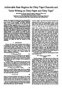
II. TIMING RECOVERY WITH LOOP-DELAY COMPENSATION Symbol timing recovery in tape read channels is usually performed by means of a 2nd-order PLL as depicted in Fig. 1. The input to the circuit is a noisy observation y k of the sampling phase of the readback signal. The PLL consists of a loop filter of the proportional-plus-integral type with coefficients α and β , followed by an integrator that represents the frequency-to-phase conversion of the voltage-controlled oscillator (VCO). The estimates at time k of the sampling phase θ k and frequency offset f k provided by the PLL are denoted by φk and ν k , respectively. In the model of Fig. 1, the total PLL loop delay is lumped into the N-th order delay element D N . As input to the loop filter, only the delayed phase-error estimate ek − N = yk − N − φk − N is available.
Fig. 1. Second-order PLL with loop delay N.
The Kalman filter formulation of a 2nd-order PLL [8] suggests that φk approximates a “predicted” estimate of θ k , i.e., φk ≅ θ k / k − N −1 . Then ek − N ≅ yk − N − θ k − N / k − 2 N −1 , and the aim of delay compensation is to add a correction term to e k − N so that the input to the loop filter becomes ek − N ≅ yk − N − θ k − N / k − N −1 . Clearly, this correction term must be equal to θ k − N / k −2 N −1 − θ k − N / k − N −1 . It is seen that θ k − N / k −2 N −1 is simply obtained from φk by delaying this signal with an N-th-order delay element. The estimation of θ k − N / k − N −1 needs to be discussed further. Because the phase is the integral of frequency,
θ k +1 = θ k + f k .
(1)
From state-prediction theory [9], the (j+1)-step forward prediction of the sampling phase at time k can be expressed
978-1-4244-4148-8/09/$25.00 ©2009 This full text paper was peer reviewed at the direction of IEEE Communications Society subject matter experts for publication in the IEEE "GLOBECOM" 2009 proceedings.
as θ k + j +1 / k = θ k + j / k + f k + j / k , where f k + j / k is a j-step forward prediction of the frequency at time k. Therefore, θ k + j − N / k − N −1 = θ k + j − N −1 / k − N −1 + f k + j − N −1 / k − N −1 . Writing this expression for j = 1 to N and substituting terms yields N
θ k − N / k − N −1 = θ k / k − N −1 −
∑ f k − j / k − N −1 .
(2)
j =1
Hence θ k / k −N −1 and all 1, 2, " , N -step predictions of the frequency offset are needed to determine θ k − N / k − N −1 . A possible approximation consists of replacing the ( N + 1 − j ) step prediction f k − j / k − N −1 with f k − j / k − N − j −1 , i.e., to use fixed (N+1)-step predictions. These predictions are available from the PLL circuit provided that ν k is regarded as an approximation to the predicted frequency-offset estimate at time k. Eq. (2) then becomes
θ k − N / k − N −1 ≅ φk −
N −1
∑ν k − j ,
(3)
j =0
where the range of the summation has been redefined to save one delay element in the implementation. The resulting PLL with delay compensation is shown in Fig. 2. After some successive linear transformation steps, this circuit is drawn as the equivalent circuit shown in Fig. 3, which may be preferred from an implementation point of view. If a satisfactory model for the evolution of the frequency offset is available, the predicted quantities can be specified further. For example, a familiar model for the frequency offset is given by the random walk process [10]
f k +1 = f k + wk ,
(4)
where wk is a sample of an additive zero-mean white Gaussian noise process with variance E{wk2 } = q . In this case, the 2nd-order PLL can be shown to be equivalent to a Kalman filter, as described, e.g., in [8], and the loop coefficients are given by the Kalman gain vector. Then, because f k + j − N / k − N −1 = f k + j − N −1 / k − N −1 , Eq. (2) becomes
θ k − N / k − N −1 = θ k / k − N −1 − N ⋅ f k / k − N −1 ,
(5)
which is identical to the solution given in [7]. Note that this solution is optimal provided that the model of Eq. (4) faithfully describes the actual frequency-offset evolution. Transfer Function Analysis The closed-loop transfer function of the 2nd-order PLL with compensated loop delay is now derived with reference to the circuit of Fig. 3. The VCO, loop filter, and delay compensation circuits have transfer functions given by
GVCO ( z ) = G LF ( z ) =
z −1 1 − z −1
,
(6)
α + ( β − α ) z −1 1 − z −1
,
1 − z −1
G DC ( z ) =
1 − (1 − α ′) z −1 − α ′z − N −1
(7)
,
(8)
respectively. In Eq. (8), the coefficient α in the delay compensation section of the PLL was replaced with α ′ , so that its effect explicitly appears in the following expression of the closed-loop PLL transfer function. From Eqs. (6)-(8), this transfer function is obtained as ′ ( z) = G PLL
α ( z − 1) + β N
2
z [( z − 1) + α ′( z − 1)] + (α − α ′)( z − 1) + β
. (9)
By setting α ′ = α , the transfer function becomes G PLL ( z ) =
α ( z − 1) + β N
z [( z − 1) 2 + α ( z − 1)] + β
.
(10)
The closed-loop transfer function of a 2nd-order PLL without loop delay is obtained by setting N = 0 in Eq. (10), i.e., Fig. 2. Delay compensation in a 2nd-order PLL with loop delay N.
G PLL − 2 nd order ( z ) =
α ( z − 1) + β ( z − 1) 2 + α ( z − 1) + β
.
(11)
Fig. 4 plots the magnitude and phase characteristics of a 2nd-order PLL (i) without loop delay [Eq. (11)], (ii) with a loop delay of N = 20 and no delay compensation [Eq. (9) with α ′ = 0 ], and (iii) with a loop delay of N = 20 and delay compensation [Eq. (10)], assuming α = 2 ×10 −2 and
β = 10 −4 . It is seen that delay compensation aims at
Fig. 3. PLL with delay compensation equivalent to the circuit of Fig. 2.
restoring the magnitude characteristic of the PLL without loop delay. In fact, it can be shown that the absolute error
978-1-4244-4148-8/09/$25.00 ©2009 This full text paper was peer reviewed at the direction of IEEE Communications Society subject matter experts for publication in the IEEE "GLOBECOM" 2009 proceedings.
from a plurality of channels and generates “global” control signals for use by the individual channels for their timing recovery functions. It achieves robust symbol timing recovery in the presence of disturbances, such as dropout events, instantaneous speed variations, nonlinear signal distortion, etc. GTC was shown to significantly improve the reliability of timing control in tape systems and is especially efficient in terms of its resilience to cycle-slip events. Two GTC schemes are particularly attractive in actual implementations: the so-called “phase-combining” scheme and the “frequency-combining” scheme. They are illustrated in Fig. 6, assuming, for the sake of drawing clarity, a two channel system. Both schemes generate a global frequencyoffset estimate, the former scheme by a weighted combining of the individual phase estimates and the latter by a weighted combining of the individual frequency estimates.
Fig. 4. PLL transfer characteristics without and with a loop delay of N = 20. (a) Magnitude responses, (b) phase responses.
Fig. 6. Global timing control shown for two channels: (a) phase combining and (b) frequency combining.
In Fig. 6, α1 , α 2 , β1 , β 2 and β denote loop-filter coefficients and w1 , w2 weighting coefficients. The inputs Fig. 5. PLL transfer characteristics without and with a loop delay of N = 30. (a) Magnitude responses, (b) phase responses.
′ ( z ) and G PLL−2 nd order ( z ) between the magnitudes of G PLL
ε=
1
∫0
′ (e j 2πf ) df (12) G PLL − 2nd order (e j 2πf ) − G PLL
is minimized for α ′ = α , i.e., G PLL (z ) gives the best match to the 2nd-order PLL without loop delay in terms of magnitude response. Fig. 5 shows similar results as Fig. 4, but assuming a loop delay of N = 30 . III. LOOP-DELAY COMPENSATION WITH GLOBAL TIMING CONTROL Global timing control (GTC) is a multichannel timingcontrol technique [5] that combines the timing information
(i )
and outputs of the loop filters are indicated by e k − N and
uk(i ) , i = 1, 2 , respectively. The computation of the weighting coefficients is explained in [5]. Loop-delay compensation is now extended to these GTC schemes. Fig. 7 shows the case of phase-combining-based GTC augmented with delay compensation. In Fig. 7(a), a single global delay-compensation circuit, indicated by dashed lines, is employed for all channels. Usually, α1 = α 2 , so that the value of the global coefficient α G can also be set equal to α1 and α 2 . In Fig. 7(b), delay compensation is performed on a per-channel basis. A third, hybrid solution is shown in Fig. 7(c) that uses the global frequency-offset estimate for the frequency term but employs per-channel phase estimates for the phase term of delay compensation. The performance of the scheme in Fig. 7(b) was observed to be somewhat superior to that of the two other schemes,
978-1-4244-4148-8/09/$25.00 ©2009 This full text paper was peer reviewed at the direction of IEEE Communications Society subject matter experts for publication in the IEEE "GLOBECOM" 2009 proceedings.
Fig. 8. Delay compensation for frequency-combining-based GTC employing hybrid global/per-channel compensation.
Fig. 7. Delay compensation for phase-combining-based GTC: (a) global, (b) per-channel, and (c) hybrid global/per-channel compensation.
with, however, a correspondingly higher implementation complexity. A detailed comparison of the respective performances will not be pursued here for lack of space. Delay compensation for GTC based on frequency combining can be developed similarly. For example, the per-channel delay compensation approach of Fig. 7(b) can also be used for frequency-combining GTC. A hybrid delay compensation scheme is shown in Fig. 8 for frequency-combining-based GTC. IV. NUMERICAL RESULTS The effectiveness of PLL delay compensation is illustrated in this section with respect to four “sets” of readback waveforms captured on state-of-the-art commercial tape drivesystems. Each set consists of the readback signals of 16 parallel data channels. Sets 1, 2 and 3 were captured at linear recording densities that are increasingly higher than that normally used by the drive, so that the operation of the read channel, and hence that of the timing recovery loops, can be
tested under stress conditions. Set 4 corresponds to recording at nominal linear density, but some of its waveforms exhibit significant distortions that cause the read channel to operate at an undesirably high bit-error-rate regime (see below). To emulate the actual Linear Tape Open (LTO) recording format [11], data were written on tape in sectors of approx. 8 Kbits, with each sector separated by special fields known in the LTO specification as the Data-Set Separator (DSS), Variable Frequency Oscillator (VFO) and Synchronization (Sync) fields. The error patterns on the detected bit sequences were parsed into long (error bursts of length 64 or larger) and short errors. Long errors and missed sectors due to missed Sync fields are mainly indicative of cycle-slip events. A software read-channel processes the 16 waveforms in parallel and delivers a set of 16 sequences of detected bits. On each channel, decision-aided interpolative timing recovery [12] is implemented; the decisions are generated from either a memoryless threshold device (slicer) or a maximum- likelihood sequence detector (MLSD) releasing early tentative decisions with a delay of Δ = 6 or 8. The well-known Mueller–Muller [13] timing-error detector is employed. The timing recovery loops are able to operate either independently on each channel or in a GTC mode. Table I summarizes the results obtained for the four sets of readback waveforms without GTC. For all cases, the delay compensation circuit of Fig. 3 was used, and the delay assumed by the compensation circuit was optimized in the range of 10 to 20 symbol intervals. The actual timing loop delay in the simulated read channel is about 15 symbol intervals. A mismatch of a few symbol intervals may exist between the actual and assumed loop delays without affecting the performance of the compensation scheme. It is seen from Table I that delay compensation results in a significant uplift in performance for all the cases. Note that the different waveform sets were not necessarily captured on the same tape drive; hence comparing the performance of one waveform set with respect to another may not be meaningful.
978-1-4244-4148-8/09/$25.00 ©2009 This full text paper was peer reviewed at the direction of IEEE Communications Society subject matter experts for publication in the IEEE "GLOBECOM" 2009 proceedings.
TABLE I: DETECTION PERFORMANCE WITHOUT GLOBAL TIMING CONTROL FOR THE FOUR WAVEFORM SETS. Decision Type for Timing Loop Slicer Set 1
MLSD Δ=6 MLSD Δ=8 Slicer
Set 2
MLSD Δ=6 MLSD Δ=8 Slicer
Set 3
MLSD Δ=6 MLSD Δ=8 Slicer
Set 4
MLSD Δ=6 MLSD Δ=8
Delay Compensation
Bit Errors
Short Errors
Long Errors
Missed Sectors
no yes no yes no yes
11,185 6,178 40,479 4,394 81,964 10,895
245 256 252 294 256 314
25 20 29 10 43 11
33 14 38 10 87 18
no yes no yes no yes
21,118 7,667 14,684 600 10,001 610
269 267 214 230 232 239
23 12 9 0 12 1
1 1 13 3 20 4
no yes no yes no yes
92,131 6,806 6,684 930 10,249 984
583 441 403 380 391 386
104 18 9 3 19 6
5 2 11 3 21 5
no yes no yes no yes
85,539 5,143 288,437 6 762,206 2,695
32 12 201 3 365 8
58 6 251 0 621 5
0 0 2 0 3 0
In Table II, the performance achieved in the presence of a GTC scheme is summarized. The scheme employing phaseerror combining and delay compensation as shown in Fig. 9(b) was implemented. The results of sets 1-3 show that, because GTC already significantly robustifies the PLL behavior by including phase-error information from the other parallel channels, the effect of delay compensation is smaller than in the cases without GTC. However, it is interesting that in some cases, such as for set 4, delay compensation still achieves significant performance advantages. V. CONCLUSIONS The attainment of high areal storage densities in tape systems critically depends upon the reliable operation of the read-channel timing recovery function. This paper has shown that the robustness of the timing recovery loop can be substantially improved by loop-delay compensation. This technique is effective in lowering the bit-error rate at the detector output as well as mitigating cycle-slip phenomena. Different solutions were described and shown to be effective for the application of loop-delay compensation in connection with global timing control. The main cost for implementing loop-delay compensation is associated with the N-stage buffering of the phase-error signal at the loop-filter input, where N denotes the amount of delay that is compensated. In a multichannel tape system, this cost is incurred on a per-channel basis if per-channel delay compensation is applied. Alternatively, the cost will be lowered if delay compensation is applied to a group of channels in connection with global timing control.
TABLE II: DETECTION PERFORMANCE WITH GLOBAL TIMING CONTROL FOR THE FOUR WAVEFORM SETS. Decision Type for Timing Loop Slicer Set 1
MLSD Δ=6 MLSD Δ=8 Slicer
Set 2
MLSD Δ=6 MLSD Δ=8 Slicer
Set 3
MLSD Δ=6 MLSD Δ=8 Slicer
Set 4
MLSD Δ=6 MLSD Δ=8
Delay Compensation
Bit Errors
Short Errors
Long Errors
Missed Sectors
no yes no yes no yes
1,025 920 1,002 1,003 983 998
232 234 231 266 238 263
15 12 14 8 14 10
0 0 0 1 2 0
no yes no yes no yes
680 626 504 556 550 552
245 232 193 210 212 216
5 2 1 1 0 1
0 0 0 0 0 0
no yes no yes no yes
1,162 1,034 866 844 910 842
451 414 342 352 368 354
7 4 2 2 2 2
0 0 1 1 0 0
no yes no yes no yes
6 2 28 2 694 2
3 1 13 1 68 1
0 0 0 0 24 0
0 0 0 0 0 0
REFERENCES [1] [2] [3] [4] [5] [6] [7]
[8] [9] [10] [11] [12] [13]
Y. Yuan, E. Kurtas, and B. V. K. Vijaya Kumar, “Performance of timing recovery methods in turbo coded magnetic recording channels,” IEEE Trans. Magn., Vol. 36, No. 5, pp. 2187-2189, Sep. 2000 A. Nayak, J. R. Barry, and S. W. McLaughlin, “Joint timing recovery and turbo equalization for coded partial response channels,” IEEE Trans. Magn., Vol. 38, No. 5, pp. 2295-2297, Sep. 2002. J. R. Barry, A. Kavcic, S. W. McLaughlin, A. Nayak, and W. Zeng, “Iterative timing recovery,” IEEE Signal Proc. Mag., Vol. 21, pp. 89102, Jan. 2004. J. Moon and J. Lee, “Decision-directed timing recovery based on maintaining multiple phase trajectories,” Proc. IEEE Globecom2006, San Francisco, CA, 2006, paper GEN04-3. S. Ölçer, J. Jelitto, and R. Hutchins, “Global timing control with applications to tape storage channels,” Proc. IEEE Globecom 2008, New Orleans, LA, 2008, paper SA09W1-1. J. W. M. Bergmans, “Effect of loop delay on stability of discrete-time PLL,” IEEE Trans. Circuits and Systems–I, Vol. 42, No. 4, pp. 229231, Apr. 1995. A. Patapoutian, “Application of Kalman filters with a loop delay in synchronization,” IEEE Trans. Commun., Vol. 50, No. 5, pp. 703-706, May 2002, and “Loop latency compensated PLL Filter,” US Patent 6,236,343B1, May 22, 2001. G. S. Christiansen, “Modeling of a PRML timing loop as a Kalman filter,” Proc. Globecom 1994, vol. 2, pp. 1157-1161, 1994. B. D. O. Anderson and J. B. Moore, Optimal Filtering, Prentice-Hall, 1979. J. W. M. Bergmans, Digital Baseband Transmission and Recording, Kluwer Academic Publishers, 1996. G. Jaquette, “LTO: A better format for mid-range tape,” IBM J. Res. Develop., Vol. 47, No.4, pp. 429-443, July 2003. F. M. Gardner, “Interpolation in digital modems - Part I: Fundamentals,” IEEE Trans. Commun., Vol. 41, pp. 501-507, Mar. 1993. K. H. Mueller and M. Muller, “Timing recovery in digital synchronous data receivers,” IEEE Trans. Commun., Vol. COM-24, No. 5, pp. 516531, May 1976.
978-1-4244-4148-8/09/$25.00 ©2009 This full text paper was peer reviewed at the direction of IEEE Communications Society subject matter experts for publication in the IEEE "GLOBECOM" 2009 proceedings.