ABSTRACT. The computation of logic-stage delays is a fundamental sub-problem for many EDA tasks. Although accurate delays can be obtained via.
Computing Logic-Stage Delays Using Circuit Simulation and Symbolic Elmore Analysis Clayton B. McDonald
Randal E. Bryant
Department of Electrical and Computer Engineering Carnegie Mellon University, Pittsburgh, PA 15213 �
clayton,bryant @ece.cmu.edu �
ABSTRACT The computation of logic-stage delays is a fundamental sub-problem for many EDA tasks. Although accurate delays can be obtained via circuit simulation, we must estimate the input assignments that will maximize the delay. With conventional methods, it is not feasible to estimate the delay for all input assignments on large sub-networks, so previous approaches have relied on heuristics. We present a symbolic algorithm that enables efficient computation of the Elmore delay under all input assignments and delay refinement using circuit-simulation. We analyze the Elmore estimate with three metrics using data extracted from symbolic timing simulations of industrial circuits.
1.
INTRODUCTION
The computation of logic-stage delays in transistor networks is a fundamental sub-problem for a number of electronic design automation tasks. Examples include static timing analysis, timing simulation, transistor-sizing optimization, and library cell characterization. Determination of the sensitizing conditions for the maximum and minimum stage delays is extremely difficult in general, and exact solutions may be impossible for large networks. Typically, stage delays are computed on channel-connected regions (CCRs), consisting of all nodes and transistors reachable from each other through transistor drain-source (channel) connections. Given a particular input transition or simultaneous set of transitions, we wish to determine the delay to the resulting transition on a designated output node. This delay value is generally dependent on the states of other inputs to the stage, as well as the initial conditions of the internal nodes. For example, Figure 1 shows a dynamic stage where the delay from a rising to pc falling is dependent on the values of b, c, and x1. Inputs b and c control the conductance of the discharge path, while the initial state of x1 affects the amount of charge that must be removed. Determining the sensitizing conditions for the minimum or maximum delay is further complicated by potential logical relationships between the inputs. This research was supported by the SRC (contract DC-068)
Permission to make digital or hard copies of all or part of this work for personal or classroom use is granted without fee provided that copies are not made or distributed for profit or commercial advantage and that copies bear this notice and the full citation on the first page. To copy otherwise, to republish, to post on servers or to redistribute to lists, requires prior specific permission and/or a fee. DAC 2001, June 18-22, 2001, Las Vegas, Nevada, USA. Copyright 2001 ACM 1-58113-297-2/01/0006 ...$5.00.
CK
pc \
a/ b
c
x1 0
Figure 1: Effects of Side-Conditions on Delay
Previously published approaches have used a combination of formal methods and heuristics. Desai and Yen [8] implemented algorithms for sensitizing the maximum delay on a specified path through a multi-CCR transistor-level network, which they decomposed into sensitizing a series of maximum delays through single CCRs. Their method utilizes Boolean functions (stored as Binary Decision Diagrams, or BDDs) to compute the set of input assignments that enable the desired input to output transition. For small CCRs, they advocate explicit enumeration of these input assignments to determine which sensitizes the largest delay. For large CCRs, they first determine the maximum-resistance driving path, and then use a greedy algorithm that attempts to select the assignment which maximizes the capacitance connected to the output node. This approach assumes that the assignment that maximizes the Elmore delay will maximize the true delay, an assumption that is challenged by our data (Section 3). Furthermore, maximizing the resistance before considering capacitances may not even lead to a maximal Elmore delay, as there might be an assignment which sensitizes a low-resistance, high-capacitance driving path with a larger RC product. Burks and Main’s approach [5] is quite similar, though they primarily focused on incorporating logical dependencies between inputs. To select the worst-case input assignment, they say only that they use a heuristic method. Our approach also uses the Elmore delay as an estimate of the true delay. However, using symbolic techniques, we can exploit the regularity of large CCRs and compute the Elmore delay exactly for all input assignments while avoiding exponential blowup for all but the most pathological cases. The primary enabler for our methodology is the Multi-Terminal Binary Decision Diagram (MTBDD) data structure [2]. Using MTBDDs, we compute the Elmore delay for all possible input assignments. We can then select one assignment for each possible delay case, and use it as stimulus for a SPICE-like simulation. Section 2 discusses the computation of the symbolic Elmore delay and its refinement to high-accuracy delay values with a SPICE-
F
x2
a=1
a
b/
out
b
x2 c=0
x1
out x1
τ
1.2
+ -
2.5
Figure 3: Example MTBDD
+
F a
Figure 2: Elmore Approximation for Logic Stage
G
H
a
a
b like simulator. We then present error-characterization data in Section 3, drawn from test-runs of our symbolic timing simulator on industrial circuit designs.
2. 2.1
0.4 1.2
1.0
2.5
STAGE-DELAY CALCULATION
1.6
2.9
3.5
Figure 4: Example MTBDD Operation
Elmore Estimate
Since our approach is based on the Elmore estimate of a logicstage’s delay, we will first present a quick review. The Elmore delay is an estimate of the dominant time constant of the step-response of an RC tree. As a result, it has been heavily utilized for estimating delays in interconnect networks. However, a number of researchers have adapted it to obtain delay estimates of single stages of MOSFET circuits [11, 6]. This is accomplished by removing non-conducting (OFF) transistors and replacing conducting (ON) transistors with simple linear resistors. At each internal node we compute a single grounded capacitance value, and then heuristically break loops of conducting transistors to complete the RC tree. This conversion process is depicted in Figure 2. Besides the obviously risky approximation of transistors by linear resistances, the Elmore estimate has several deficiencies when used for logic stages. First, it assumes that the inputs switch instantaneously at time zero. To incorporate the effects of non-zero rise/fall times, we can effectively modify the resistance representing the turning-on transistor to reflect its reduced drive-capacity or calculate an empirical penalty to be added onto the final delay estimate. The second major assumption is that of a single driving voltage source. This can be a significant difficulty in analyzing stages where multiple pulldown paths can be activated simultaneously, or for ratioed circuits where pullup and pulldown paths are “fighting” each other. Again, empirical approximations can be made to incorporate these effects, as was done by Chu[6]. Since our symbolic Elmore analysis procedure is based on Chu’s, it implements these enhancements.
2.2
b
MTBDDs
Previously published approaches to stage-delay computation have utilized symbolic techniques to handle logical restrictions on input patterns with considerable success. However, they have had to resort to heuristic methods for representing real-valued functions, such as resistance, capacitance and delay. The primary enabler for our approach, and the key to extending symbolic techniques to this real-valued domain, is the Multi-Terminal Binary Decision Diagram (MTBDD) [2]. MTBDDs are generalizations of BDDs that allow an arbitrary number of real-valued terminals. For example, the MTBDD in Figure 3 represents the function having two inputs and . To de-
�
�
termine the return value for any given input assignment, we work downwards from the root, following the solid arc from nodes assigned 1 and the dashed arcs from nodes assigned 0. We can see that when either or is 1, and otherwise. Computation on MTBDDs can be accomplished using the function MtbddApply, which is virtually identical to the well-known BDD Apply function[3]. It takes as arguments an operator and two operands, and returns an MTBDD representing the result for all input assignments. For example, Figure 4 shows two input MTBDDs and , and the MTBDD that would result from computing MtbddApply(+, , ). MtbddApply has worst-case complexity , where represents the number of terminals in MTBDD . Using MtbddApply, we can perform any algebraic operations necessary to compute series and parallel resistances, RC products, and other quantities needed for our analysis. For example, since Elmore delays in digital networks are computed by replacing transistors with switched resistors, we can represent its symbolic resistance by an MTBDD which returns infinity where the transistor is off, and its equivalent conducting resistance when it is on (Figure 5). Then, using MtbddApply calls, we can compute arbitrary parallel and series combinations of these symbolic resistors as shown in Figure 6. Throughout this paper, we will denote BDDs and MTBDDs in boldface (i.e. ), while scalar values will appear in normal type. We will also often utilize infix notation rather than explicit calls to MtbddApply, such that MtbddApply . In some cases it will be convenient to specify trivial MTBDDs, consisting only of a single terminal node, in brackets (i.e. ).
������
� �
�
��� � �
�� �
����� �� ��� � � �
� ���� �� � � ! "� $#
������
R
a
3.2K
5/1
a
a inf Figure 5: Representing FETs
3.2
R
1 2 3 4 5 6 7 8 9 10 11 12
a
a
5/1 5/1
b
b
b
inf
3.2
1.6
Figure 6: Symbolic FET Analysis ck a
ck b a
b
c
b
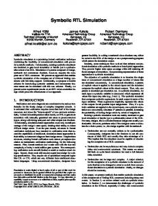
Figure 8: Delay Refinement
d c d 1ns
Figure 7: Example
2.3
� , � ��� � � ) ���������� ��� � ! � � # � while �� ��� ����� ! � # � �� ��� ��� � �����! � MtbddMinTerminal � "$#&%('*) � MtbddEqual ��� ���� ��� �+� � ���, � -�. ��/ � GetRandomCube "$#&%('0) 1 nodes 2435� � 2 � 7 '*)8%(9 �+-�. �:/ � 2 � 6 � Evaluate � ��; = �,