The light boxes are to be considered as mirrors which reflect the signal path. It is obvious then ... (a) Bipartite graph of the first stage of the network shown in. Fig.
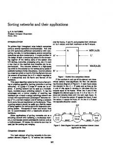
Crossover networks and their optical implementation Jurgen Jahns and Miles J. Murdocca
Crossover networks are introduced as a new type of interconnection network for applications in optical computing, optical switching, and signal processing. Crossover networks belong to the class of multistage
interconnection network. Two variations are presented, the half-crossover network and the full crossover
Crossover network. An optical system which implements both networks is proposed and demonstrated. networks can be implemented using the full space-bandwidth product of the optical system with minimal loss of light. It is shown that crossover networks are isomorphic to other multistage networks such as the Banyan
and perfect shuffle.
I. Free-Space Architectures for Optical Digital Computers
The interest attracted by optical digital computing is mainly stimulated by its potential to implement massively parallel architectures. This holds especially for free-space optical systems where 2-D arrays of logic
elements can be connected using imaging setups. Free-space optical interconnections also offer the potential to do the communications in a computer at an extremely high temporal bandwidth without introducing problems such as clock skew or crosstalk.1
The use of optical imaging setups for parallel interconnects, however, limits the variety of feasible topologies to regular interconnects. The space-bandwidth product (SBP) of an optical system, i.e., the number of connections, reduces with increasing complexity of the interconnection scheme. For this reason, interest has grown in regular interconnection networks such as the perfect shuffle
2
or the Banyan.
3
The use of regular
networks seems to limit the flexibility of designing a digital general purpose computer. It has been shown, however, that they can be used for general purpose
computers efficiently in terms of gate count and throughput.4 The perfect shuffle and the Banyan both belong to the class of multistage interconnection network (MINs). For interconnecting N inputs to N outputs, perfect shuffle and Banyan require log2 (N) stages. Throughout this paper we shall assume that N is a power of 2. MINs are of great importance, for example, in digital signal processing for the design of fast algorithms 5 or in computing for the realization of sorting networks. 6 Various authors have addressed the use of multistage networks in optical data processing.7 -12
One problem which arises for the implementation operations.
Optical systems, however, offer a large
SBP only for space-invariant operations. It is, therefore, necessary to find a way of implementing a specific
network without losing too much of the space-bandwidth product. In this paper, we present crossover interconnects as a new interconnection
network, which is an interesting
alternative to the Banyan and the perfect shuffle. Crossover networks offer the potential for a simple optical implementation. Specifically, it is possible to use the full SBP of an optical system. This means that the number of connections is limited, in principle, only by diffraction.
Two versions of crossover networks
will be presented in Sec. II, the half-crossover network and the full crossover network. An optical implementation for both, which is based on a Michelson setup, is
proposed in Sec. III. Special optical components are used which are called prism gratings. Practical limitations for the implementation of the network arising from the use of these components are discussed in Sec. IV. In Sec. V we shall present several experimental results, and finally, in Sec. VI we show that crossover
networks are isomorphic to the Banyan and the perfect shuffle. I.
Crossover Networks
This work was initially stimulated by a proposal for a
VLSI interconnection network which was made by Wise.13 This proposal was motivated by the need to have wires of exactly the same length to reduce path length differences between signals. The diagram of Wise's network is shown in Fig. 1.
The functional boxes as indicated by the shaded rectangles are not important for our discussion. Their function may vary with the specific application for which the network is used. Each box may in fact be composed of a mininetwork
The authors are with AT&T Bell Laboratories, Jersey 07733. Received 2 November 1987. 0003-6935/88/153155-06$02.00/0. © 1988 Optical Society of America.
Holmdel, New
of
MINs is the fact that they represent space-variant
of its own.
The light
boxes are to be considered as mirrors which reflect the signal path. It is obvious then that this network is composed of signal paths of identical lengths. The name crossover network illustrates the pattern of the signal paths. 1 August1988
Vol. 27, No. 15 / APPLIEDOPTICS
3155
m=O
11
1
2
2
3
m=2
13
4
4
5 6
5 6 7
7 Fig. 1.
m=1
Crossover network for VLSI circuits.' 3
Fig. 3.
Half-crossover network for eight input ports. The index m indicates the number of a specific stage.
m=0
a
m=1
m=2
b
Fig. 2. (a) Bipartite graph of the first stage of the network shown in Fig. 1; (b) rearranged graph. Fig. 4. Full crossover network for N = 8.
The diagram in Fig. 1 might lend itself to a wave-
guide optical implementation.
The lines would di-
rectly represent the waveguides. For a free-space optical implementation it is useful to rearrange the interconnections. To this end we represent the first stage of the network shown in Fig. 1 by a bipartite graph, which shows the input ports of the stage, the output ports, and the connections between them [Fig. 2(a)]. The input ports are numbered by integers which run from 0 to 7. On the output side, the boxes are labeled according to where the connections originate. Figure 2(b) shows the rearranged version of the graph. On the output side still the same combinations of numbers appear. However, they now appear in a different order. We note that the graph in Fig. 2(b) is very regularly structured. The interconnection pattern consists of straight-through connections and crossover connections. The straight-through connections can be implemented optically by a simple imaging step. The crossover can be implemented by imag-
ing as well, but a spatial inversion with respect to the first image has to be introduced. We shall discuss a possibility to achieve this inversion in some detail in the next section. We consider the diagram in Fig. 2(b) to be the first stage of our new network and assign to it the index m = 0. The higher stages are then obtained by the following rule. For stage m we subdivide the input into 2m partitions. For each partition, we copy the input pixels to the output side. Furthermore, we apply a cross3156
APPLIEDOPTICS / Vol. 27, No. 15 / 1 August 1988
over within each partition. The whole network consists of log2 (N) stages where N is the width of the network. For N = 8, the complete network is shown in Fig. 3. The boxes were labeled according to their physical addresses. We will refer to the network shown in Fig. 3 as the half crossover network (HCN).
A variation of the half-crossover network is obtained in the followingway. We subdivide the input ports to the mth stage into 2m+1partitions. Then we replace the straight-through connections with crossover connections within each partition. This results in the full crossover network (FCN) shown in Fig. 4.
For simplicity, the networks are shown in Figs. 3 and 4 for 1-D inputs. For 2-D input data it is necessary to modify the operation of the network so that first the rows are processed in log2 (N) steps. Then columns are processed using also log2 (N) stages. Ill.
Optical Implementation of the Crossover Network
Figure 5 shows an optical setup which implements one stage of the crossover network.
It is based on a
Michelson setup. It should be noted, however, that the performance of the setup is not based on interference. The use of optical architectures
which are de-
rived from two-beam interferometers is simply a con-
venient way of implementing the splitting and
combining of 2-D arrays of pixels. The setup shown in Fig. 5 implements the HCN. As we shall see, only a
minor change has to be made to realize the connections for the FCN.
St
S
prism
P1 input
I mirror P2
lens
P4 Fig. 5.
output
Optical setup for the implementation
m=1
m=0
of one stage.
m=2 Fig. 7.
6
Operation of the reflective 900 prism.
.16V^V^V^11
01234567 a Fig. 6.
01234567
01234567
0
Flipping of the input pixels using partitioned
c prisms.
The full crossover network can be realized with the same setup as shown in Fig. 5. The only change which
has to be made is that the mirror in P2 is replaced by a prism grating. IV. Practical Limitations for the Implementation of Crossover Networks
The beam splitter BS splits the input signal into two different paths. The planes P, P2 , P3 , and P 4 are related to each other by imaging steps. The path Pi P2 - P4 with a mirror in P2 implements the straightthrough connections. The path Pi - P3 - P4 implements the crossover connections. This is achieved for the first stage of the network by placing a reflective 900 prism in P3 . The effect of the prism is visualized in Fig. 6(a). It illustrates the flipping of the input pixels with respect to one symmetry axis as required for the first stage. To implement the crossover connections for the higher stages, wehave to partition the prism. A double prism is required for the second stage (m = 1), a quadruple prism for the third stage (m = 2), etc. [see Figs. 6(b) and (c)].
Figure 7 depicts the use of the 900 prism by showing the light paths. Light that would be focused to a position S in the back focal plane of the lens is reflected twice and is sent back into the optical system as if it would emerge from position S'. S and S' are symmetric with respect to the center position of the prism. It is important to note that, for light traveling to different positions, i.e., for different pixels, the path lengths to travel are exactly the same. Therefore, no relative time delays are introduced between different signals. Two features should also be mentioned. First, the setup shown in Fig. 5 implements one stage of the network. For the complete network one has to use log2 (N) such setups. Second, the use of polarization optics allowsus to implement each stage without losing light energy except for Fresnel losses.
In this section we will address a problem which occurs when using prism gratings for implementation of the higher stages (m # 0) of the network. The situation is shown in Fig. 8(a). Here the optical setup for implementing the second stage is shown with a double prism in plane P3. For simplification the optical path P, - P3 is displayed in an unfolded way. As shown in the drawing, some of the light which is sup-
posed to be focused down to a spot close to the center will hit the wrong facet of the prism grating. After reflection from this facet the light will be reflected out of the optical system and will be lost. This situation occurs when the numerical aperture large.
of lens 3 is too
The situation will be most severe for the pixel closest to the optical axis. Only light traveling under an angle which is smaller than fl/2 will arrive at this spot R. Assuming a pixel separation in the input array of 6x
and an optical setup with a 1:1magnification, R will be at a distance Ax/2from the center. To avoid losses the numerical aperture of the light on the right-hand side of the optical setup has to be smaller than a certain maximum value N.A.3,maxThis value is determined by N.A. 3 max
=
tan(0/2).
(1)
The value for 4/2 depends on the stage number m and on the size N of the input array. To compute f(m)/2 we have to make a few geometrical considerations.
The height of the prism which is used for the mth stage is 1 August 1988 / Vol. 27, No. 15 / APPLIEDOPTICS
3157
Pi
N spots
lens 1
N
lens 3
P3
ax/2 Nkx
I
I I l
-
f1
f3 (a)
lens 1
P1
lens 3
P3
Wi I
I I I
.....
I..........
NA, fi
Fig. 8.
R
T Vax/2 (a)
z
f3 (b) (a) Light losses due to a large numerical aperture.
The
situation is shown for the second stage. Dark lines indicate the light path for a fullyopened aperture. The dashed lines indicate the light path for a reduced aperture. The reflected light rays are not shown for simplicity. (b) Reduction of the numerical aperture using mag-
nification.
h(m) = (N/2m+l)bx, m = 0....M,
(2)
where M is defined as M = log2(N)- 1.
(3)
From this it followsthat
ax 2=
N.A.3,ma.() (m) =
=
-
of 640,um (b). =
..
M.
(4)
Equation (4) indicates that the problem is most severe for the second stage (m = 1) where N.A.3,maxtakes on
very small values. For example, for an array with N = 64 pixels in one dimension one obtains N.A.3,max = 1/ 32. This would be a severe restriction to the use of crossover interconnects especially, since the SBP of
the setup is proportional to the numerical aperture. Without taking any measures one would either lose light for the pixels close to the center or be restricted to relatively large pixels with a diameter 2X/N.A.3 ,maxHowever, there is a simple way to circumvent this problem completely. By using magnification it is possible to reduce the numerical aperture of the light cones. Magnification is introduced by making the focal length f3 of lens 3 larger than the focal length f of lens 1 [Fig. 8(b)]. The spot pattern will then be magnified by a factor V: V
f-
fl
(5)
Accordingly the numerical aperture of the light on the right-hand side of the setup will be reduced by V. 3158
(b)
Fig. 9. Experimental setup (a) and the prism grating with a period
APPLIEDOPTICS / Vol. 27, No. 15 / 1 August 1988
N.A 3 = N.A.
(6)
This results in a larger value for N.A.3,max: N.A.3,max(m) = 2m
-
(7)
As an example we consider again the case that N = 64 and that on the input side we use a lens with a numerical aperture N.A., = 0.25. This corresponds to a lens
with /4. Then for the second stage of the network (m = 1) a magnification factor V = 8 would be required to
achieve a lossless implementation. For the higher stages the required magnification is reduced significantly. We would like to add the remark that besides saving light energy the magnification trick has another beneficial side effect. Since the spot pattern is magnified it is possible to use relatively coarse prism gratings which are easier to fabricate than very fine ones. Therefore, magnification can be used specifically to select a certain period for the prism grating. It is also worthwhile to note that the overall magnification between planes P and P 4 is not affected by the focal length of lens 3. Instead it is strictly determined
(C)
(b)
(a) Fig. 10.
Experimental results:
(a) input object:
Chinese character (light).
Output of the first (b) and second (c) stage.
by the ratio 4/fl where f is the focal length of the lens near plane P4 (Fig. 5). V.
Experimental Results
The experimental results which are presented in this section were obtained by using the Michelson setup shown in Fig. 5 and prism gratings. The photograph in Fig. 9(a) shows the actual optical system.
Two
different prism gratings were used for the experiments. One had a period of 640 gim,the second had a period of 10 gim. Figure 9(b) shows a photograph of the coarse grating.
Using the 640-gimgrating the first and the second stages of the half-crossover network were implemented. For clarity, only the output patterns due to the
f
crossover connections are shown in Figs. 10(b) and (c).
In both cases the input pattern was the Chinese character shown in Fig. 10(a). It consists of 10-gm spots on a grid of 32 X 32 pixels. The spots were separated by 20 gAm. The same grating was used for implementa-
-*
x
Fig. 11. Output pattern of an experiment with the 10-,umprism grating.
tion of both stages. For the first stage a 1:1 magnification was used and a 2:1 magnification for the second
Isomorphism of Crossover Networks with Banyan VI. and Perfect Shuffle
stage.
Finally, we would like to point out that the crossover networks are topologically equivalent to other MINs like the Banyan and the perfect shuffle. This is important because it allows Banyan-based algorithms such as the fast Fourier transformation to be transformed to a crossover-based implementation.
With regard to the question how practical prism gratings are in general, a grating with a very fine period of 10 gm was tested.
A regular spot pattern was used
as the input. The spots were (3 gm)2 in size. They were separated by 10gm in the x direction and by 5 Am
in the y direction. The setup was used to implement the crossover connections of the final stage of the network. After reflection from the grating the output pattern looks the same as the input pattern. The output pattern is shown in Fig. 11. Obviously, the
pattern has a good contrast indicating that the use of
First, we note that each stage of the crossover can be
described mathematically in terms of two permutations. In the followingwe denote the binary address of the nth pixel (0• n • N - 1) by (n). For example, for N = 8 the binary address is a 3-tuple (n2 ,n1 ,no), where
prism gratings is feasible even in the range of a few
micrometers. For this experiment, microscope objective lenses (/2) were used at their diffraction limit (X= 0.633 gim). Some losses occurred due to light surrounding the center spots of the Airy disks hitting the corners of the prism grating and scattering out of the optical system.
n=4n 2 +2n 1+n 0, nk=Oorl.
(8)
(n) = (n 2,nl,no)
(9)
We put and write
(n)k
when we invert the kth bit; e.g., (n) 1 = (n 2,n 1,no).
1 August 1988 / Vol. 27, No. 15 / APPLIEDOPTICS
(10) 3159
property can be shown to hold for the Banyan. Therefore, the equivalence between the HCN and the Banyan is proved according to Ref. 14. We would like to add the remark that a formal proof for the isomorphism between the half-crossover and the Banyan was given by Cloonan. 1 5 VII.
Conclusion
The crossover network was introduced as a new mul-
tistage interconnection network with applications for optical computing and photonic switching. We have presented two variations of crossover networks, the half- and the full crossover. Both are isomorphic to the more familiar Banyan and perfect shuffle. The
Fig. 12. Diagram for the Banyan network (N = 8).
stage
stage
m
m+1
crossover network was designed specifically for a free-
space optical implementation. An optical system for the implementation of crossover interconnections was proposed and demonstrated. It makes use of special optical components which are called prism gratings. The use of these prism gratings is possible down to very small feature sizes in the micron range. It is possible to implement the crossover network with a large space-bandwidth product and a high light efficiency. The authors would like to thank Vijay Kumar for bringing their attention to the work of D.S. Wise and Alan Huang for helpful comments on this subject.
Fig. 13. Buddy property of switching nodes.
References
With this notation we can describe the permutations ll~m ) and I(m) for the mth stage of the HCN as follows: II(): (n)
I(m):
(n)
-
(n);
(11)
(n)Mm.
(12)
For showing the isomorphism of the crossover and other MINs we make use of a proof which was given by Agrawal.14 It says that two MINs are equivalent if two conditions are fulfilled. First, both have to be constructed out of nodes with two inputs and two outputs. This is obviously the case for the crossover networks (Figs. 3 and 4) as well as for the Banyan network which
is shown in Fig. 12. Second, there has to hold a socalled buddy condition. This means that each pair of nodes of stage m is connected with only one pair of nodes of stage m + 1. This buddy property is represented graphically in Fig. 13.
In a formal way the buddy property can be shown for the half-crossover network by using the permutation formalism introduced earlier. Equations (11) and (12) show that the pixel with address (n) in the mth stage is connected to two pixels in the m + 1st stage with addresses (n) and (n)Mm. The same is true for the pixel with the address (n)M-m in stage m because H('m):(n)m-,n
II(m):(n)Mm,
(Mm
(13)
(n).
(14)
From Eqs. (13) and (14) we can conclude that the crossover network falls into the class of MIN satisfying both conditions as given above. Similarly the buddy 3160
APPLIEDOPTICS / Vol. 27, No. 15 / 1 August 1988
1. A. Huang, "Architectural Considerations Involved in the Design of an Optical Digital Computer," Proc. IEEE 72, 780 (1984).
2. H. S. Stone, "Parallel Processing with the Perfect Shuffle," IEEE Trans. Comput. C-20, No. 2, 153 (1971). 3. L. Goke and G. Lipovski, "Banyan Networks for Partitioning
Multiprocessor Systems," in Proceedings, First Annual Computing Architecture Conference(1973),pp. 21-28. 4. M. J. Murdocca, A. Huang, J. Jahns, and N. Streibl, "Optical Design of Programmable (1988).
Logic Arrays," Appl. Opt. 27, 1651
5. E. 0. Brigham, The Fast FourierTransform (Prentice-Hall, Englewood Cliffs, NJ, 1974).
6. D. J. Kuck, The Structure of Computers and Computations (Wiley, New York, 1978).
7. J. Jahns, "Efficient Hadamard Transformation for Large Images," Signal Process. 5, 75 (1983).
8. A. W. Lohmann, W. Storck, and G. Stucke, "Optical Perfect Shuffle," Appl. Opt. 25, 1530 (1986). 9. G. Eichmann and Y. Li, "Compact Optical Generalized Perfect Shuffle," Appl. Opt. 26, 1167 (1987). 10. G. E. Lohman and A. W. Lohmann, "Shuffle Communication Component for Optical Parallel Processing," J. Opt. Soc. Am. A 4(13), P106 (1987).
11. K.-H. Brenner and A. Huang, "Optical Implementation of the Perfect Shuffle," Appl. Opt. 27, 135 (1988).
12. J. Jahns, "Optical Implementation of the Banyan Network," to be published. 13. D. S. Wise, "Compact Layouts of Banyan/FFT
Networks," in
VLSI Systems and Computations, H. T. Kung, B. Sproull, and G. Steele, Eds. (Computer Science Press, Rockville, MD, 1981), pp. 186-195. 14. D. P. Agrawal, "Graph Theoretical Analysis and Design of Mul-
tistage Interconnection Networks," IEEE Trans. Comput. C-32, 637 (1983). 15. T. J. Cloonan, "Topological Equivalence of Simple Crossover
and Banyan Networks," to be published.