Abstract - In this paper DAC static parameter definitions are evaluated highlighting their ... and gain, INL (Integral NonLinearity), DNL (Differential NonLinearity).
DAC static parameter specifications - some critical notes E. Balestrieri, S. Moisa, S. Rapuano Faculty of Engineering, University of Sannio, Piazza Roma, 82100, Benevento, Italy E-mail: {balestrieri, moisa, rapuano}@unisannio.it Ph.: +39 0824305817; Fax: +39 0824305840
Abstract - In this paper DAC static parameter definitions are evaluated highlighting their differences and similarities. Great attention has been paid to the most commonly used specifications. As a result of this analysis a unique set of DAC specifications is proposed considering that each parameter has to be unambiguously defined and practically measurable. I. Introduction The exponential growth of electronic systems including digital signal processing led to an increasing interest in data converters. In many systems the digital information must be converted to the analog domain through a Digital-to-Analog Converter (DAC). Target applications for DACs include 3G cellular infrastructure, broadband wireless access, satellite communications, high-resolution imaging, medical equipment and test instrumentation. In practice, DACs performance are affected by their non ideal transfer characteristic. The converters’ differences from an ideal behavior are characterized by a number of performance specifications that determine the DAC static and dynamic performance. Different applications have different performance requirements. To preserve the sound quality in audio, for example, the preeminent target is to have a high dynamic range with little or no distortion. For video systems, instead, the DAC linearity is the crucial parameter to ensure systems harmonic a good picture quality. Hence selecting the right DAC for a particular application needs the knowledge of the performance requirements this device has to meet and to understand the product specifications provided by manufacturers. Consequently the identification of the basic DAC performance parameters and their unambiguous definition become absolutely necessary. The relevance of this topic is proved by the current project of the Waveform Measurement and Analysis Technical Committee (TC-10) of the IEEE Instrumentation and Measurement Society aiming to produce a new standard defining terminology and test methods for DACs [1]. In the years different definitions for the same DAC parameters were proposed, often not precisely defined, causing possible misinterpretation of the real device performance. In this paper several DAC static performance parameter definitions taken from existing standards, scientific literature and manufacturers’ documentation are collected, compared and discussed to propose a unique and unambiguous set of parameter definitions. This could be useful both to manufacturers and to users for evaluating and comparing existing devices. During the research work, great attention has been paid to the most commonly used specifications focusing on the following parameters: resolution, full scale range, LSB (Least Significant Bit), offset and gain, INL (Integral NonLinearity), DNL (Differential NonLinearity). This paper is a part of a research project oriented to provide a comprehensive overview on DAC topics [2]. The DAC static specifications should be chosen considering that each parameter has to be unambiguously defined and practically measurable. The measurableness is an essential requirement in production testing and prototype characterization and for the device evaluation. For this reason each definition should be joined with its measurement unit taking as reference the International System of Units (SI). The final set of DAC specifications is proposed taking into account the most used definitions coming from the collected references. For each parameter the existing definitions have been entirely adopted, modified or completely rewritten in order to satisfy the above reported requirements. Since some DAC specifications (where possible), could be derived from the ADC ones with the appropriate changes, the IEEE Standard for Terminology and Test Methods for Analog-to-Digital Converters (IEEE Std. 1241) [3] has been used as guideline. In the following the paper has been divided in five sections, each of them analyzes a single parameter and proposes a possible new definition for further discussions. II. Resolution The DAC resolution can be expressed in different forms. The IEC 60748-4 [4] distinguishes among the numerical, the analog and the relative resolution clarifying that “the terms for these different forms may all be shortened to “resolution” if no ambiguity is likely to occur (for example, when the
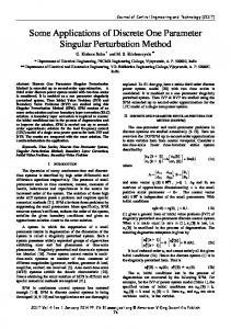
dimension of the term is also given)”. The numerical resolution is defined as “the number of digits in the chosen numbering system necessary to express the total number of steps” of the transfer characteristic, where a step “represents both a digital input code and the corresponding discrete analogue output value”. The analog resolution is defined as the nominal value of the difference in step value between two adjacent steps, (step height) often used as a reference unit named LSB. Finally the relative resolution is “the ratio between the analog resolution and the full scale range (practical or nominal)”. In scientific literature the shortened term resolution is used in the numerical or in the analog sense [5]. Fig. 1. Ideal DAC transfer function. The most commonly used definition of resolution provided by manufacturers’ datasheets is the numerical resolution expressed in bits [6]-[9]. The IEEE Std. 1241 [3] doesn’t define the term resolution, but uses the LSB definition to indicate the analog resolution reported in [4]. The numerical and the analog resolution are the definitions that most often appear in the references. The first is determined by architecture, is dimensionless and not measurable. The second is measurable and is expressed either in volt or ampere. Considering that the analog resolution can be defined through the LSB definition and that the specifications set, purpose of this paper, must include univocal definition of each parameter, the numerical sense of resolution is recommended for adoption. However, the IEC 60748-4 [4] numerical resolution definition requires to know what is a step. A better definition could be the following: “The number of bits used to produce each analog output level. The higher is the number of bits, the smaller is the analog (voltage or current) output step that could be output level generated. An N-bit resolution implies producing 2N distinct analog levels” The above definition doesn’t require the knowledge of other DAC parameters and simply highlights the differences between DACs with different resolutions. III. Full scale range The Full Scale Range (FSR) is the difference between the maximum and minimum analog output values that the DAC is specified to provide, usually the max and min values are also specified. For an N bit DAC these values are usually given as the ones matching with code 0 and 2N. The code 2N is used only to define the ideal DAC transfer function not existing in the practical usage. So the maximum analog output of the converter never quite reaches such level output defined as analog Full Scale (FS). In particular, the maximum value that the DAC can provide corresponds to FS (1-2-N) (Fig.1) [10]. For example, a unipolar 12-bit DAC with FS=10 V has a maximum analog value of +10 ∗ (1-2-12) V= +9.99756 V. For bipolar DAC using 1’s complement or sign-magnitude coding the minimum analog output is different of one LSB from the nominal negative FS. The above quoted coding schemes, in fact, having two different code words to represent the zero level (Tab. I), provide a symmetrical transfer function [11]. In Tab. I an example of bipolar coding schemes is reported for a DAC with +FS=5 V and -FS=-5 V. The IEC 60748-4 [4] distinguishes the FSR in practical and nominal. The first is “the total range of analogue values that corresponds to the ideal straight line. Using a straight binary in bit code formats, for a DAC”: FSR = (2N-1) ∗ (nominal value of step height).
(1)
The nominal FSR is “the total range in analogue values that theoretically can be coded with constant accuracy by the total number of steps. Using a straight binary in bit code formats, for a DAC”: FSR (nom) = 2N ∗ (nominal value of step height).
(2)
The IEEE Std. 1241 [3] defines the FSR as “the difference between the most positive and most negative analog inputs of a converter’s operating range”. A formula is also reported: FSR = (2N) ∗ (ideal code bin width) for an N bit ADC.
(3)
From formula (3) the FSR definition seems to refer to the difference between the theoretical maximum and the minimum analog input values, but the quoted “converter’s operating range” seems to refer to the practical full scale range as defined from IEC 60748-4. Most manufacturers’ datasheets use the term full scale range to refer to the difference between the theoretical maximum and the minimum DAC analog output levels, someone [12] using the term “nominal full scale range” to refer to the practical full scale range as defined in IEC 60748-4 [4]. The two definitions above quoted provide two different analog values, with the same dimension. Even though for high resolution DAC there is a small difference between these analog values, a clear distinction between the two meanings is necessary to understand the actual device working and to correctly test it. For this reason two definitions are proposed as follows: “The full scale range is the difference between the output levels ideally corresponding to the minimum and maximum input codes. It can be expressed either as a voltage or a current”. “The practical full scale range is the difference between the most positive and most negative analog outputs that can be achieved from the converter. It can be expressed either as a voltage or a current”. IV. LSB This term can have two meanings depending on the context in which it is used. The IEC 60748-4 [4] defines the abbreviation LSB as “the bit that has the lowest positional weight in a natural binary numeral”. The unit symbol LSB, instead, is defined as “the unit symbol for the magnitude of the analogue resolution of a linear converter, which serves as reference unit to express the magnitude of other analogue quantities of that same converter, especially of analogue errors, as multiples or submultiples of the magnitude of the analogue resolution”. The IEEE Std. 1241 [3] defines the LSB as “synonymous with one ideal code bin width” that is “the ideal full-scale input range divided by the total number of code bins”. The second LSB meaning is missing. Manufacturers’ datasheets use both LSB meanings [5,6,11], leaving the context clarifies which is the intended significance. When a distinction is adopted, the wordings “LSB weight”, “LSB analog value” or “nominal LSB magnitude” are used to refer to the unit symbol LSB as defined in the IEC 60748-4 [4]. Of the two definitions one is dimensionless, while the other one can be a voltage or a current value depending on the DAC output. So two different definitions are necessary to discriminate the two meanings. In particular the LSB and the analog LSB are defined as follow: “In the binary number scheme, LSB is the bit position, producing the smallest output level”. “The analog LSB is the smallest DAC output level that is unambiguously distinguishable over the entire full scale range of the converter. It can be expressed either as a voltage or a current”. V. Gain and offset These specifications depend on which DAC transfer curve is used as a reference. In particular, the manner in which the actual characteristic is matched to the ideal characteristic must be clearly specified to define gain and offset unambiguously [13]. The general transfer curve of the DAC can be represented by the following equation: y = mx + b
(4)
where DAC gain is m and DAC offset is b. There are two main methods for determining gain and offset. The forner is the endpoint method which sets gain based on the minimum scale and FS points. Offset is determined from the intercept of the line (Fig. 2.a). The latter is the best-fit line. The m and b (gain and offset) parameters are set based on the minimum mean squared error from line to sample (Fig. 2.b) [14]. The IEC 60748-4 [4] defines the gain as “the slope of the straight line of the transfer diagram or of a specified part of it expressed as the quotient of a change in analogue output quantity, by the change in digital input quantity, stated as number of steps, producing it”. From the reported definition, the ideal straight line is traced between “the specified points for the most
positive (least-negative) and the most negative (least positive) nominal step values respectively”. As a consequence, the endpoint method seems to be adopted for the gain value determination. The IEC 60748-4 [4] gain definition doesn’t clarify how to build the straight line, anyway the best-fit method isn’t considered. Moreover, the slope of the Fig.2. a) Endpoint method; b) Best-fit method. straight line representing the entire transfer characteristic is different from the slope values achieved considering only a part of the transfer diagram, so the definition is ambiguous. The IEC 60748-4 [4] defines also offset error and gain error introducing a gain point and offset point for adjustable DAC. The first one is “a point in the transfer diagram corresponding to the step value of the step for which the offset error is specified, and by reference to which the offset adjustment must be performed”. The gain point is “a point in the transfer diagram corresponding to the step value of the step for which the gain error is specified, and in reference to which the gain adjustment is performed”. The gain error is defined as “the difference between the actual step value and the nominal step value in the transfer diagram at the specified gain point, after the offset error has been adjusted to zero”. The offset error is defined as “the difference between the actual step value and the nominal step value at the offset point”. These definitions seem considering the possibility to determine offset and gain errors referring to any point of the transfer diagram. Although the IEC standard in the chapter devoted to measuring methods suggests, in a note, where the gain and offset points are generally located on the transfer characteristic. In any case the quoted above parameters are not clearly defined. It’s well known that the offset error should affect all codes by the same amount, but the actual offset value changes with the offset point because “the difference between the actual and the nominal step value” can include linearity errors. So defining a univocal offset point is essential to achieve an unambiguous offset error definition. In the same way, gain error has different value for different gain point (smaller values nearest the first codes). Also in this case a univocal gain error definition is necessary. The IEEE Std. 1241 [4] reports two different definitions for gain and offset: independently based and terminal based. In the first instance gain and offset are “the values by which the input values are multiplied and then to which the input values are added, respectively, to minimize the mean squared deviation from the output values”. In the second instance gain and offset are “the values by which the input values are multiplied and then to which the input values are added, respectively, to cause the deviations from the output values to be zero at the terminal points, that is, at the first and last codes”. Recognizing in independently based and terminal based gain and offset, respectively the best-fit and the endpoint method is immediate. Although IEEE 1241 [4] doesn’t define offset and gain error, it’s trivial obtaining them as the difference between their real and ideal values. Several DAC manufacturers relate offset error to the digital input zero [15,16,17] and define gain error as the difference between the output voltage (or current) with full scale input code and the ideal voltage (or current) that should exist with a full scale input code [15,18], [17] specifying that the offset has to be already removed. Another definition expressing the same concept is provided by Analog Devices, which defines gain error as the difference between the actual and ideal output span where the actual span is determined by the output when all inputs are set to “1”, minus the output when all inputs are set to “0” [16]. The output span is clearly the quoted FSR. Definitions strongly dependent from the input code can’t be used for all DACs (they don’t work for complementary coding DAC). The definition for gain error [15,17,18] considers the error at the last code without taking into account the other ones. From what quoted above, some considerations can be done. Defining together gain and offset takes into account the strong relation existing between this two parameters and the method used to achieve the DAC transfer function. The definitions have to be independent from the input code used and valid for unipolar and bipolar DACs. The IEEE Std. 1241 [3] for offset and gain seem to satisfy these requirements but they should be clarified by joining them with the DAC transfer function equations. Therefore, these could be adopted for the corresponding DACs parameters with additional comments. For example, the DAC offset and offset error are identical when the ideal offset is 0. Many DACs are commonly used in application requiring a single power supply, in this case the ideal offset should be nonzero, but the offset error should always be zero [19]. Offset can be expressed in LSB, ampere, volt, %FSR and %FS. The gain error can be both the difference between the real and the ideal gain of the DAC (dimensionless) and also defined as a percent:
⎛G ⎞ gain _ error = ⎜⎜ actual − 1⎟⎟ ⋅ 100% G ⎝ ideal ⎠
(5)
Taking into account the previous considerations, the proposed definitions for gain and offset are the following: “(Independently based) Gain and offset are the values by which the output values are multiplied and then to which the output values are added, respectively, to minimize the mean squared deviation from the ideal output values”. “(Terminal-based) Gain and offset are the values by which the output values are multiplied and then to which the output values are added, respectively, to cause the deviations from the ideal outputs to be zero at the terminal points, that is, at the first and last codes”. VI. Differential and Integral NonLinearity While gain and offset represent the linearity errors of a DAC, the DNL and the INL represent its nonlinearity errors. Non-linearity errors should be evaluated once gain and offset errors have been canceled by trimming (if possible), or compensated for by mathematical operations, so that they can be distinguished from linear errors [20]. DNL is computed by the difference between the analog output values corresponding to two successive input codes referred to one LSB. The IEC 60748-4 [4] defines DNL as “the difference between the actual step height and the ideal value (1 LSB)”, specifying also that a DNL greater then 1 LSB can lead to non-monotonicity of a DAC. The IEEE 1241 defines DNL of an ADC as “the difference, after correcting for static gain, between a specified code bin width and the ideal code bin width, divided by the ideal code bin width. When given as one number without code bin specification, it is the maximum differential nonlinearity of the entire range”. The DNL formula as expressed in [3] requires only the static gain correction, because since the offset error is the same for all codes, it is both added and subtracted and therefore cancelled. From both definitions it’s clear that DNL value depends also on the definition of the average LSB size. To highlight this matter [19] introduces three basic types of DNL calculation method: best-fit, endpoint and absolute. Best-fit DNL uses the best-fit line’s slope to calculate the average LSB size; endpoint DNL is calculated by dividing the full-scale range by the number of transitions; the absolute DNL technique uses the ideal LSB size derived from the ideal maximum and minimum full-scale values. The order of methods from most relaxed to most demanding is best-fit, endpoint and absolute. The three methods result in nearly identical results, as long as the DAC doesn’t exhibit grotesque gain or linearity errors so the choice of technique is actually not so important for DNL as for INL calculation. Most datasheets define DNL as the difference between the measured output voltage or current difference between two adjacent codes without specifying if the gain and offset correction has been carried out. This is an important information because, as quoted above, non-linearity errors should be evaluated once gain and offset errors have been evaluated. The IEEE 1241 definition could be adopted with the following modifications: “Differential nonlinearity is the difference, after correcting for static gain, between a specified code bin and the next code, divided by the ideal code bin width. When given as one number without code bin specification, it is the maximum differential nonlinearity of the entire range. DNL is expressed in LSB.”. While DNL is a measurement of the uniformity in the voltage or current DAC step from one code to the next, INL is a measure of accumulated errors in the step sizes. INL is obtained by comparing the actual DAC characteristic and a reference DAC line, so the value of this parameter is strongly dependent on the line chosen as reference. IEC 60748 [4] proposes two different INL definitions valid for linear and adjustable DAC. The endpoint linearity error is “the difference between the actual and the nominal step value, after offset and gain errors have been adjusted to zero”. The best-straight-line linearity error is “the difference between the actual and nominal step value, after offset and gain error have been adjusted to minimize the extreme value of this difference (either positive or negative)”. IEEE 1241 [3] defines INL as “the difference between the ideal and measured code transition levels after correcting for static gain and offset. Integral nonlinearity is usually expressed as a percentage of full scale or in units of LSBs. It will be independently based or terminal-based depending on how static gain and offset are defined. When the integral nonlinearity is given as one number without code bin specification, it is the maximum integral nonlinearity of the entire range”. It’s worth to note that the INL value depends not only on the considered reference line. In fact, since it is calculated after gain and offset error correction, the definition of gain and offset parameters could lead to different INL values. For example in a datasheet from Analog Devices [6] the INL is defined as
“a measure of the maximum deviation of the DAC transfer function from a straight line passing through the endpoints of the transfer function. It is measured after allowing for zero and full-scale errors” where the full-scale error is “a measure of the output error when the amplifier output is at full scale (for the bipolar output range full scale is either positive or negative full scale). It is measured with respect to the reference input voltage and includes the offset errors”. Moreover, the zero error is defined as “a combination of the offset errors of the DAC and output amplifier”, for unipolar input and “a combination of offset errors in the DAC, amplifier offset and mismatch in the application resistors around the amplifier”. Manufacturer’s datasheets adopt both INL definitions, although the endpoint is the most adopted [6,9], often without specifying if the gain and offset errors have been canceled or not [6,7,8]. Sometimes understanding the particular INL definition adopted isn’t possible because it isn’t reported [7] or it is referred to a generic “best straight line” [8]. As quoted above, gain, offset and INL definition are strictly related and need to be clearly defined. A good definition for INL, is that proposed by IEEE 1241, because it specifies that INL must be calculated after correcting gain and offset and that its value is dependent on how this two parameters have been defined. This definition also agrees with the gain and offset definition previously proposed in this paper. For these reasons the proposed definition is: “The Integral NonLinearity is the difference between the ideal and measured code transition levels after correcting for static gain and offset. Integral nonlinearity is usually expressed as a percentage of full scale or in units of LSBs. It will be independently based or terminal-based depending on how static gain and offset are defined. When the integral nonlinearity is given as one number without code bin specification, it is the maximum integral nonlinearity of the entire range”. VII. Conclusions In this paper the need for a unique set of DAC specifications including both the end-user and the manufacturers point of view has been highlighted. Several DAC static parameter definitions coming from different sources are collected, compared and discussed in order to propose a unique set of definitions. The final set of DAC static specifications has been achieved considering that each parameter has to be unambiguously defined and practically measurable. Future developments will concern the analysis of the dynamic parameter definition also taking into account DYNAD [21] and IEC 60748-4-3 (including ADC and DAC dynamic specifications). References [1] IEEE Std. 1658 Draft, “IEEE Standard for terminology and test methods for digital-to-analog converters”, 2005. [2] E.Balestrieri, P.Daponte, S.Rapuano, “Digital to analog converter: a metrological overview”, 9th Workshop on ADC Modelling and Testing, Athens, Greece, September 29th - October 1st, 2004. [3] IEEE Std. 1241, “IEEE Standard for terminology an test methods for analog-to-digital converters”, 2000. [4] IEC 60748-4, Semiconductor Devices – Integrated Circuits – Part 4: Interface integrated circuits – Sec. 2: Blank detail specification for linear analogue-to-digital converters, Second edition, 1997. [5] K.L.Parthasarathy, R.L.Geiger, "Unambiguous characterization and specification of D/A converter performance", Proc. of 2000 Midwest Symposium on Circuits and Systems, pp. 890-894, August 2000. [6] Analog Device, AD7237A/AD7247A datasheet available at www.analog.com. [7] Maxim, MAX5773-MAX5775 datasheet available at www.maxim-ic.com. [8] Intersil, AD7520, AD7521 datasheet available at www.intersil.com. [9] Texas Instruments, TLV5614IYE datasheet available at www.ti.com. [10] D. A. Johns, K. Martin, “Analog integrated circuit design”, John Wiley & Sons, Inc., 1997. [11] Intersil, AN 002, “Principles of data acquisition and conversion”, Oct. 1986, www.intersil.com. [12] Analog Device, DAC8043 datasheet available at www.analog.com. [13] S.K.Tewksbury, F.C.Meyer, D.C.Rollenhagen, H.K.Schoenwetter, T.M.Souders, “Terminology related to the Performance of S/H, A/D and D/A Circuits”, IEEE Tran. on Circuits and Systems, vol. CAS-25, No.7, pp.419426, July 1978. [14] Bill Jasper, “Practical telecom DAC testing”, www.testedgeinc.com. [15] Texas Instruments, “Understanding data converters”, MicroSystem Mixed-Signal Data Converters: Application Note, July 1995, available at www.ti.com . [16] Analog Device, “Data converters: High speed Digital-to-Analog converters Glossary”, available at www.analog.com. [17] Maxim, ADC and DAC Glossary, Application Note 641, December 2000, available at www.maxim-ic.com. [18] National Semiconductor, “D/A converters - Definition of terms”, May 1999, available at www.national.com. [19] M. Burns, G. W. Roberts, “An Introduction To Mixed-Signal IC Test and Measurement”, Oxford University Press, 2001. [20] Atmel, “Data converter terminology”, Application Note, available at www.atmel.com. [21] Project DYNAD— SMT4-CT98-2214 — Draft standard, Version 3.4, 2001.