Design for Test of Crystal Oscillators: A Case Study. MARINA SANTO-ZARNIK. HIPOT HYB, Trubarjeva 7, ËSentjernej, Slovenia. FRANC NOVAK AND SRE ...
P1: KCU JOURNAL OF ELECTRONIC TESTING: Theory and Applications
KL491-02-Santo
September 3, 1997
14:57
JOURNAL OF ELECTRONIC TESTING: Theory and Applications 11, 109–117 (1997) c 1997 Kluwer Academic Publishers. Manufactured in The Netherlands. °
Design for Test of Crystal Oscillators: A Case Study MARINA SANTO-ZARNIK ˇ HIPOT HYB, Trubarjeva 7, Sentjernej, Slovenia ˇ ˇ FRANC NOVAK AND SRECKO MACEK Joˇzef Stefan Institute, Jamova 39, 1000 Ljubljana, Slovenia Received September 30, 1996; Revised May 22, 1997 Editor: M. Soma
Abstract. A feasibility study of design-for-testability (DFT) of a voltage controlled crystal oscillator with built-in MOS switches to increase its observability and controllability is presented. The primary aim was to assess to what extent the operation of the circuit is changed when the switches are introduced. The possibility of non-destructive localization of faulty components in the provided test modes and the temperature/frequency characteristics measurements are briefly described. Finally, on the basis of the presented experimental work, a design-for-test procedure for crystal oscillator circuits is summarized. The work was performed in a development phase of a voltage controlled temperature compensated crystal oscillator. Keywords: analog circuits, crystal oscillators, design-for-test, fault diagnosis
1.
Introduction
The growing complexity of integrated circuits, minimization and the advent of surface-mounted device (SMD) technology make the problem of testing the assembled boards more and more difficult. Design for test (DFT) techniques are employed to keep the complexity of tests at a reasonable level. DFT in digital domain is a mature research area with established general guidelines and well-known practical solutions [1–3], some of them even standardized, like for example IEEE standards 1149.1 and 1149.5. On the other hand, analog DFT is still emergent [4, 5], and as noticed in [6], the general problem of DFT for analog circuits is almost certainly intractable. Hence it is more realistic to expect partial solutions suitable for specific classes of circuits. A number of such DFT solutions have recently been proposed [7–10]. In this paper we present a feasibility study of the design for test of a voltage controlled temperature
compensated Pierce crystal oscillator with built-in MOS switches which are used to increase its controllability and observability. By introducing the DFT switches a circuit can be partitioned into parts that can be easily tested and fault isolation can be accomplished at the level of individual circuit components. However, an important question is if the impact of the DFT switches can be compensated so that the circuit operates within the specified tolerances. An experimental study of the impact of the DFT switches on the operation of the oscillator circuit is the main issue of this paper. The conclusions of the study are summarized in a general design-for-test procedure. The paper is organized as follows. In Section 2, the oscillator circuit designed for testability and diagnosability is presented and the test modes corresponding to the selected switch positions are described. In Section 3, the impact of switches on the operation of the oscillator within the specified temperature range is studied and experimental results are given. The
P1: KCU JOURNAL OF ELECTRONIC TESTING: Theory and Applications
110
KL491-02-Santo
September 3, 1997
14:57
Santo-Zarnik, Novak and Maˇcek
localization of faulty passive components in the oscillator circuit is discussed in Section 4. Measurements of frequency/temperature characteristics of crystal units are described in Section 5. In Section 6, the designfor-test procedure for crystal oscillator circuits is summarized, and finally, in Section 7, concluding remarks are given. 2.
DFT of Oscillator Circuit
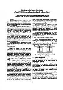
The block diagram of a crystal oscillator can be represented as a closed loop system with an amplifier of an open-loop gain A, and a feedback network containing the crystal with a transfer function β(ω). In order that the circuit oscillates, the following conditions must be satisfied [11, 12]:
Fig. 2.
Block diagram of VCTCXO.
• the total phase shift around the closed loop must be an integer multiple of 360◦ , • the loop gain at the frequency where the phase requirements are met must be greater or equal to unity. A faulty circuit component may cause improper operation such that the circuit either does not oscillate or its frequency differs from the expected one. Since the oscillator circuit is a closed loop system, isolation of faulty components is a difficult task. The application of the design-for-test methodologies may simplify the troubleshooting and provide means for automated diagnostics. A straightforward idea is to break the closed loop of the oscillator such that external stimuli can be applied at some external pin of the modified circuit and output observed at some other external pin. Like in [6], MOS switches can be employed for this purpose. The situation is depicted in Fig. 1. If input stimuli are applied at X 1 we can observe the response of the amplifier part of the oscillator at X 2 . DC and AC responses at significant frequencies can be used in fault localization.
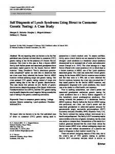
Fig. 3.
Oscillator with the DFT switches.
Conversely, the feedback β(ω) as a passive frequency selective network and can be regarded in the frequency domain as a filter circuit. Diagnostic conclusions can be drawn from the known transfer characteristics and measured response to the known input stimuli. The application of the above idea has been studied in a development phase of a voltage controlled temperature compensated crystal oscillator (VCTCXO) depicted in Fig. 2. Its kernel, the Pierce crystal oscillator (presented with dashed block) is shown in detail in Fig. 3. In our case study, switches S1 , S2 , S3 and S4 are used to open (or short) chosen paths of the circuit. Notice that the voltage control input presented as Vc can be used in the test mode to apply stimuli to the transistor stage or to observe the response of the feedback path. 2.1.
Test Modes
The circuit operation can be analyzed in the following modes:
Fig. 1.
Block diagram of an oscillator.
• Normal Mode: (S1 ON, S2 OFF, S3 OFF, S4 ON), operation of the oscillator circuit is measured,
P1: KCU JOURNAL OF ELECTRONIC TESTING: Theory and Applications
KL491-02-Santo
September 3, 1997
14:57
Design for Test of Crystal Oscillators • Test Mode 1: (S1 OFF, S2 OFF), feedback cut off, analysis of the amplifier part. It comprises the following cases: 1. (S3 OFF, S4 OFF), R6 is measured at the output. 2. (S3 ON, S4 OFF), values of R7 /R8 and R11 are verified at the input. 3. (S3 ON, S4 ON), R6 /R10 is determined by DC analysis. Since the value of R6 has been measured in test mode 1 (case 1) the value of R10 can be verified. AC analysis is performed to measure operating conditions of transistor loaded by C2 . • Test Mode 2: (S1 OFF, S2 ON, S4 OFF), analysis of the feedback circuit, crystal unit disconnected. It comprises the following two cases: 1. (S3 OFF), R6 k R9 is measured. Since R6 has been verified in test mode 1, R9 is verified. 2. (S3 ON), frequency characteristics of the RC feedback path is measured. Values of C1 , C2 , and C3 are checked. Some Further Details on Test Mode 2. The equivalent circuit of the oscillator in test mode 2 (case 2) is shown in Fig. 4. Its transition function H (s) = Vout (s)/Vin (s) is given by: H (S) =
1 R S10 R11 C1 C2
1
·³
s+
R78 +R11 C1 R78 R11
´
s
·³
s2 + s
C2 R69 +C3 R69 +R S 0 C3 1
R S 0 C2 C3 R69 1
+
1 R S 0 C2 C3 R69
´
1
where R78 denotes R7 k R8 , and R69 denotes R6 k R9 . The impedance of a switch Si , denoted by R Si , when turned ON can be modeled as a pure resistance for lower frequencies. At higher frequencies, the capacitive effect of switches in ON and OFF positions should be considered as an additional part of C1 and C2 . Notice
Fig. 4.
Equivalent circuit in the test mode 2, case 2.
111
that since R S3 ¿ R7 k R8 , its impact is negligible and hence omitted in Fig. 4. Since in our case R9 À R6 and R9 , R6 À R S2 , R6 and R9 are presented as R6 k R9 . 3.
Analysis of the Impact of the DFT Switches
The components of the crystal oscillator circuit shown in Figs. 2 and 3, are related by: 3≤
g21 C2 ≤ 15 g L C1
1 1 1 1 = + + CL C1 C2 C3 where g21 is the transconductance of the transistor, g L is the load seen by the collector and C L is the load capacitance of the crystal. C1 , C2 , C3 refer to the capacitances in Fig. 3. The above gain and phase shift relations have been obtained following the approach of derivation of the Y-parameter equations for the Pierce oscillator given in [11]. The upper and lower bounds of the gain relation have been chosen in accordance with practical estimation of the overall loop gain value. Any changes of the parameters in the above expressions obviously impact the operation of the oscillator. In the worst case the closed loop gain may decrease to the point where the circuit cannot oscillate. Otherwise if the total external capacitance to the crystal differs from the specified C L , the circuit oscillates at some frequency different from the nominal one. In practice, the values of the components normally vary within the specified tolerance ranges. In the production process of oscillator circuits with the requirements of frequency tolerances lower than the tolerances of the crystal units at 25◦ C, an adequate reserve must be provided in the values of capacitances to meet in a simple way the condition for the oscillation at the nominal frequency. In our case, the initial value of C2 is designed below the value computed from the above expressions. The final adjustment is accomplished by increasing the value of C2 . The DFT switches contribute to the changes of the parameters and hence affect the operation of the oscillator. In the following we study the operation of the oscillator with inserted DFT switches in order to investigate whether the normal circuit operation can be restored. Experiments have been performed on a 4 MHz and a 16.384 MHz oscillator implemented on a FR4
P1: KCU JOURNAL OF ELECTRONIC TESTING: Theory and Applications
112
KL491-02-Santo
September 3, 1997
14:57
Santo-Zarnik, Novak and Maˇcek
laminate (which is a common substrate for printed circuit boards) with SMD components. In both cases, transistor BFS17 and varicap diode BB619 were used. Inserted CMOS switches were of the type HEF 4066 B. At this stage, temperature compensation part has not been included. Temperature stability (in the range of 0–50◦ C) of the employed 4 MHz crystal is ±20 ppm, and that of 16.384 MHz ±3 ppm, respectively. Measurements of the circuit operation have been performed at Tamb of 25◦ C ± 2 degrees, where frequency tolerance is better than ±10 ppm (for 4 MHz crystal unit), and ±5 ppm (for 16.384 MHz crystal unit), respectively. By introducing switches S1 and S2 to the 4 MHz oscillator circuit the frequency decreased for approx. 112 ppm (measured at the MOS supply voltage VDD = 5 V), and for approx. 106 ppm (at VDD = 15 V). If only switches S3 and S4 were inserted, the frequency decreased for about 20 ppm (at VDD = 5 V), and 9 ppm (at VDD = 15 V). Finally, if all four switches were inserted the frequency changed for −137 ppm (at VDD = 5 V), and for −113 ppm (at VDD = 15 V), hence the effect of switches seems to be cumulative. Further experiments have been done in the case of 16.384 MHz oscillator. At VDD = 5 V the circuit did not oscillate, due to the impact of the inserted switches at this frequency. By increasing VDD , the circuit oscillated stable at VDD above 9 V, where the resistance of the switch RON falls to about 90 ohms. At VDD = 15 V (RON = 60 ohms) the circuit oscillated within −100 ppm which falls within the range of the measurements of the 4 MHz oscillator. Table 1 presents the measured frequency of the 16.384 MHz oscillator as a function of V [DD] of the inserted DFT switches. The frequency of the circuit before any DFT switches were inserted was 16.383 993 MHz.
Experiments have shown that the circuit with inserted DFT switches oscillates. The change of the frequency of oscillation must be considered early in the design of the circuit. In our particular case the oscillator circuit has been first adjusted to oscillate at its nominal frequency and then the DFT switches were inserted. The frequency change has been compensated for by decreasing the value of C2 . Precautions must be taken to minimize the effects of the DFT switches in the feedback path which results in a change of the gain and in a phase shift. The capacitive character of a switch becomes more important at lower values of C L and higher pulling sensitivity of the crystal unit. Some designs of oscillator circuits may also be sensitive to the switch leakage current. Further work on this issue can be directed considering [13–15]. Besides, at higher frequencies, a decrease in the OFF isolation may also become the limiting factor on the performance [15]. In critical applications, frequency stability can be achieved by employing more sophisticated switches like the 1H5140 (or AD7510) series [13]. JFET DG181 is also under consideration. The changes in the ambient temperature affect the frequency of a crystal oscillator. Among the circuit elements, the crystal is most sensitive to the changes in temperature, however other components can also be affected. Some measurements of oscillation frequency at various temperatures have been performed. Figure 5 depicts the frequency/temperature characteristics for the 4 MHz oscillator without DFT switches, and with inserted DFT switches in the temperature range 0–50◦ C. Notice that the oscillation frequency in the case with DFT switches is about 450 Hz lower, yet the shapes of the curves in both cases closely resemble. (Note that the left and the right hand scales are shifted
Table 1. Measured frequency of the oscillator circuit: 16.38 MHz + f i , i = 0, . . . , 3. f 0 [Hz]
f 1 [Hz]
f 2 [Hz]
f 3 [Hz]
4F [ppm]
10
3993
2777
3820
2329
−101
15
3993
2837
3844
2386
−98
20
3993
2903
3862
2423
−96
VDD [V]
These terms are used in the table above: VDD : MOS supply voltage. f 0 : Frequency of oscillator without switches. f 1 : Frequency of oscillator with S1 , S2 . f 2 : Frequency of oscillator with S3 , S4 . f 3 : Frequency of oscillator with S1 , S2 , S3 , S4 . 4F: Frequency change when all the switches are employed.
Fig. 5.
4 MHz oscillator: frequency/temperature characteristics.
P1: KCU JOURNAL OF ELECTRONIC TESTING: Theory and Applications
KL491-02-Santo
September 3, 1997
14:57
Design for Test of Crystal Oscillators
Fig. 6. tics.
16.384 MHz oscillator: frequency/temperature characteris-
against each other by 445 Hz.) By varying the value of C2 the curve corresponding to DFT switches can get close to the original (without DFT switches). From this point, the temperature compensation can be realized in the same way as without DFT switches. The same measurements have been repeated with the 16.384 MHz oscillator. The results are shown in Fig. 6. (The left and the right hand scales are shifted against each other by 500 Hz.) Again, the change of frequency can be compensated for by varying C2 . The impact of switches at higher temperatures affects the shape of the curve more than in the 4 MHz case. However, the temperature compensation from this point is feasible and can be done similar to the case without DFT switches.
4.
Localization of Parametric Faults in Passive Circuit Components
By applying test modes 1 and 2, localization of parametric faults of resistors is straightforward. Feedback path analysis is used in localization of parametric faults of capacitors. Here, the impact of the DFT switches on the gain and phase characteristics must be considered. Simulation results (where the switches were modeled as pure resistances) are shown in Fig. 7. The impact of switches becomes apparent at frequencies above 2 MHz. Measurements of the prototype circuit fit closely the simulations (maximum gain difference