University of Nebraska - Lincoln
DigitalCommons@University of Nebraska - Lincoln CSE Conference and Workshop Papers
Computer Science and Engineering, Department of
1-1-1991
DESIGN FOR TESTABILITY AND TEST GENERATION WITH TWO CLOCKS Vishwani D. Agrawal AT&T Bell Laboratories Murray Hill, NJ
Sharad C. Seth University of Nebraska - Lincoln,
[email protected]
Jitender S. Deogun University of Nebraska - Lincoln,
[email protected]
Follow this and additional works at: http://digitalcommons.unl.edu/cseconfwork Part of the Computer Sciences Commons Agrawal, Vishwani D.; Seth, Sharad C.; and Deogun, Jitender S., "DESIGN FOR TESTABILITY AND TEST GENERATION WITH TWO CLOCKS" (1991). CSE Conference and Workshop Papers. Paper 55. http://digitalcommons.unl.edu/cseconfwork/55
This Article is brought to you for free and open access by the Computer Science and Engineering, Department of at DigitalCommons@University of Nebraska - Lincoln. It has been accepted for inclusion in CSE Conference and Workshop Papers by an authorized administrator of DigitalCommons@University of Nebraska - Lincoln.
Proceedings, Fourth CSI/IEEE International Symposium on VLSI Design, 1991. doi: 10.1109/ISVD.1991.185102
DESIGN FOR TESTABILITY AND TEST GENERATION WITH TWO CLOCKS Vishwani D. Agrawal AT&T Bell Laboratories Munay Hill, NJ 07974, USA
Sharad C. Seth and Jitender S. Deogun Dept. of Computer Science and Eng. University of Nebraska Lincoln. NE 68588. USA
ABSTRACT - We propose a novel design for testability method that enhances the controllabiUty of storage elements by use of additional clock lines Our scheme is applicable to synchronous circuits but is otherwise transparent to the designer. The associated area and speed penalties are minimal compared to scan based methods, however, a sequential ATPG system is necessary for test generation. The basic idea Is to use independent clock lines to control disjoint groups of flip-flops. No cyclic path are permitted among the flip-flops of the same group. During testing, a selected group can be made to hold its state by disabling its clock lines In the normal mode, all clock lines carry the same system clock signal. With the appropriate partitioning of flip-flops, the length of the vector sequence produced by the test generator for a fault is drastically reduced. An n-stage binary counter is used for experimental verification of reduction in test length by the proposed technique.
generation. Previous proposals on selective controllability [3] are based on scan type of design. In fact, they are quite similar to the currently popular boundary scan idea [4]. The method presented in this paper only requires non-scan flip-flops. 2. CLOCK CONTROL FOR TESTABILITY
1. INTRODUCTION The search for a good design for testability (DFT) scheme may be viewed as finding a set of rules that impose minimal constrain on the creative freedom of the designer. For example, an asynchronous design can be made more manageable by insisting that all feedback cycles be broken by the insertion of clocked flip-flops (FF’s). This rule has a profound effect in simplifying the behavior of the circuit. To analyze an asynchronous circuit. one must, in effect, consider a finer timing (the ”gate clock); for synchronous circuits, it is sufficient to consider only the coarse timing (the circuit clock). Conversion to synchronous designs, however, is not enough to solve the testability problem. Synchronous circuits may still have very long test sequences, in some cases, too long to rule out gate-level automatic test pattern generation (ATPG) [l]. In general, there is evidence to suggest that the complexity of sequential ATPG is determined essentially by the lengths of test sequences required for individual faults [2]. The main purpose of the DFT scheme suggested in this paper is to reduce the required test lengths, thereby simplifying test
TH0340-0/0000/0112$01.OO 0 1991 IEEE
112
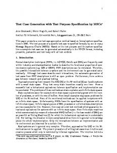
We will illuseate a new multiclock DIT scheme for the simplest case of two clocks shown in Fig. 1. In the standard (Huffman) model, a circuit is partitioned into its combinational logic block and storage elements. In our model the latter is further divided into two groups. The first group of flip-flops (FF’s) is clocked by and the second group of FF’s is clocked by q2. The two clocks are derived from the system clock (I$) by the simple selection logic shown in the figure. The clock select signals, S1 and S2, determine the mode in which the circuit would operate at any given time. The four possible modes of operation can be selected as shown in Table 1. In the normal mode the system clock controls all FF’s as in a singleclock synchronous circuit. The two test modes, clock-1 and clock-2, are symmetrical. When clock-1 test mode is on, the FF’s in the first group me allowed to change their states according to the values determined by the logic; the FF’s in the second group have their clocks disabled and they must hold their current states independent of the values on their data inputs. The situation is reversed in the clock-2 test mode. In the hold mode all the clocks are disabled and the circuit state cannot change. Table 1 - Two-clock operating modes 1 ~
s1 1 1
0 0
s2 1
0 1 0
I
Mode Normal Test, clock-1 Test, clock-2 Hold
I
In terms of the finite state machine theory, the grouping of FF’s in Fig. 1 decomposes the original state machine into two components, M1 and M2, as shown in Fig. 2. Each
d’ lp
COMBINATIONAI m I c
I I‘91~ .
?r” 1
the grouping of FF’s. The routing overhead here could be .. “edby a placement procedure that may take account of
.
the specific FF grouping. It is obvious from the figure that the scheme may not entail any time penalties.
Criterha for Partitioning FF’s. With reference to Fig. 2, the goal of partitioning should be that any desired circuit state (sl, s2) could be reached with minimum effort while using only the structural knowledge of the circuit. This is reasonable since most curzent ATF’G algorithms operate only on such information about a circuit. Before proceeding further with our discussion, we introduce a directed graph representation of a circuit and background information on definite machines.
11
I
($2)
A directed graph representation of a synchronous sequential circuit was introduced in [2]. A FF (or state variable) i in the circuit is represented by a vertex v i in the graph. A directed edge from vertex vi to vertex vi implies a combinational path from FF i to FF j in the circuit. Only the memory elements and dependencies between memory elements are explicitly represented in thii graph. If the circuit has FF’s other than the D-type,we would convert them to equivalent implementation in terms of D-FF’s before constructing the graph. A sequential machine M is called a definite machine of order p if p is the least integer, so that the present state of M can be determined uniquely from the knowledge of the last p input to M [5]. A definite machine of order p is often called a p-definite machine. Since the knowledge of any p past inputs is always sufficient to completely specify the present state of a p-definite machine, any such machine can always be realized as a cascade connection of p delay elements to store the last p input values and a combinational circuit that generates the specified output. Conversely, any circuit with n FF’s, whose graph contains no cycles, will be p-definite with pSn. From the defiition, a p-definite circuit can always be initialized by a sequence of length less than or equal to p.
Fig. 1: The twoclock DFT model. component machine can communicate its state information to the other component machine but only one component machine can change its state in a test mode. Since the state S 2 of M2 is held fixed in the clock-1 mode, we can regard the states of M1 as defining a partition of the states of the original machine. Each block of the partition is defied by a constant value of S2. Similarly, the states of M2 & f i e another partition of the states of the original machine. Each block of states in a partition defies a submachine, that is, if the test mode was held unchanged, all transitions between states are confiied to the states of the currently defied partition block. By switching test modes, however, it is possible to navigate to other states of the original machine.
A partitioning of the FF’s into multiple groups can be shown by node labels 1, 2, etc., in the graph representation. From the testability viewpoint. we claim that a good criterion for node labeling is that it should break as many directed cycles in the graph as possible, where, a cycle is considered broken if not all the nodes in the cycle are identically labeled. If all cycles can be broken, each component machine, controlled by its own independent clock (e.g. M1 and M2 in Fig. 2), can be run as a definite machine in a test mode.
Fig. 2: Machine decomposition with two clocks. Any DFT scheme introduces a certain area overhead and possibly a speed penalty. However, these are insignificant for our scheme as can be readily seen from Fig. 1. The area overhead has three components: clock select logic, clock distribution, and the two select inputs. The clock select logic is minimal. The clock distribution overhead comes from added constraints in routing the two clocks: the original clock distribution tree must be replaced by two subtrees determined by
Not all cycles can be broken, however, with a fixed number of clocks. For example, a common implementation of an n-stage synchronous binary counter involves only self-loops that cannot be broken by any number of clocks. Each stage of the counter is affected by the combined state of all the previous stages and the highest order stage requires O(2”) inputs to control its value. The goal of the multi-clock DFT in thii case would be to contain the combinatorial explosion of state space
113
3of6
by breaking long chains of identically clocked FF's. Let us assume that under the primary criterion, the available clocks have been used to break BS many cycles of length two or more as possible. We condense the resulting directed graph by identifying its strongly connected components (the nodes in each such component must be identically labeled) and collapsing them into singleton nodes. If a strongly connected component had k nodes, we associate a weight 2' to its corresponding collapsed node. All other nodes represent transparent FF's (unit delays) and are assigned a weight of 1. A secondary criterion for flipflop partitioning may now be stated as follows: minimize the weighted sum of any chain of identically labeled nodes in the graph. Thus, for the counter circuit, this criterion would require successive stages to be clocked differently. We illustrate the twoclock DFI' scheme by means of two examples.
Example I : Consider the state machine described by Table 2. It has a Synchronizing sequence of length 4,namely, 0.1,l.O. Miczo [l] uses this example to emphasize that the existence of a synchronizing sequence is not a sufficient condition for automatic test pattem generation; a proper state assignment (if one exists at all) is equally necessary [6]. In particular, for the above machine, he shows that the assignment of Table 3 is particularly bad. With this assignment, a gate-level test generation algorithm using three signal values (0,1, and X), will not be able to initialize the above machine into a known state.
lead the machine to the final state So. Further, the first three inputs in either case defme a partial synchronizing sequence that uniquely sets Y, to 1. No similar or shorter sequence exists in the normal mode to permit partial synchronization.
Exumpfe 2: Consider an n-stage synchronous counter circuit with a reset to the all-zero state. Let y o , yl, ..., yn-l represent the counter bits from the lowest to the highest order. The minimum number of clock cycles to toggle yi. starting from the reset state is obviously 2'. This means that the test length for the fault line y i s-a-0 will be exponential in i. The following lemma shows that this length can be considerably reduced by the two-clock scheme. Lemma I : An upper bound on the test length for the fault y i s-a-0 in a synchronous counter with two clocks is 1+'
L(i) = 2 and
- 1, i f i is even, i-1 L ( i ) = 3(2 ) - 1, if i is odd.
Y1
Table 2 - State table for Example 1 0
1 s2 s3
SO s2
Circuit graph
Table 3 - An improper state assignment
SO S1 s2
s3
Yz 0 1 1 0
Fig. 3: Example 1 circuit and its graph.
Y1 1 0 1 0
An implementation of the machine with the given state assignment is shown in Fig. 3 along with the corresponding graph. The graph contains self-loops on each node as well as a cycle of length 2 between the two nodes. We break the larger cycle by assigning Q 1 to FF-1 and 4i2 to FF-2. Now, the behavior of the circuit in the two modes can be deduced from the two state tables shown in Fig. 4. The corresponding synchronization tree appears in Fig. 5. In the tree, the edges are labeled as x i where x is the input value and i denotes the test mode (clock I$') used. There are two synchronizing sequences of length 4 O2,l2,ll,O2 and 11,12,11,02. Both
Proof: Partition the FF's in the counter stages into two group: {YO,Y~,... .yair ... I and (y1.y3, ... ,~2i+lr... 1. Let the first group be clocked by $, and the second group by Q 2 . Let C ( j ) represent the minimum number of clock cycles (of q 1 or Q 2 ) needed to toggle y j for j = 0, 1, ..., n-1. We know that C ( 0 ) is 1 since only one 9, cycle (with the data input 1) will toggle the least significant bit. Similarly, C(l) is 2; in this case we need to apply followed by Qz while holding the data input high. In general, we can write the following recursive relation between C( j ) and C ( j - 1 ): C ( j ) = C(j-1)
+
p$J
2
(1)
where, is the highest integer that is less than or equal to x. This is because just before yj-l toggles all preceding stages
I14
I 4 of 6
State Encoding:
state y2 y1 I
I
Mode State Table
SO
Q2 Mode State Table 0 1 Fig. 5: Test mode synchronizing tree for Example 1.
Fig. 4: Test mode state tables for Example 1 circuit. must be all-one. After it toggles. all preceding stages that are even-distance away from the (j-1)-stage change to 0 while those that are odd-distance away remain at 1. There are exactly p =
1 9 1
stages of the fmt kind and these are all
clocked identically, say, by clock Q k where k is either 1 or 2. By running 2’- 1 cyclcs of Q k while holding the data input high, we can tum all 0 stages to 1 (they would be incremented like a k-bit counter). Further, all stages that stored 1 originally, remain unchanged as their clocking is disabled. One more clock cycle after this will toggle yj. This justifies the recurrence in Eq. (1) from which the bound in the lemma follows immediately. 3. TEST GENERATION WITH TWO CLOCKS
In a synchronous clocked circuit, the primary input (PI) signals and flip-flops (FF’s) normally change once during a period of the clock. The combinational logic of the circuit receives its inputs from PI and FF’s and it feeds into the primary outputs and FF’s. In the interval between the instances when FF’s change their state, the circuit can be analyzed like combinational logic. Since all FF’s change only once in the clock period, it is only when the time advances to the next
clock period, that the FF must be updated. For test generation, the combinational logic can be duplicated for each clock period. Each duplicated block contains its PI and PO and FF signals flow between the blocks. With this model, it is possible to generate tests using a combinational test generation algorithm [7]. For generating tests with two clocks, we expand the combinational logic in two dimensions. This is shown in Fig. 6. Clock-1 periods are shown along the x-direction and Clock-2 periods are along the negative ydirection. Each block is a copy of the combinational logic. The block i , j is the circuit in the i -th period of Clock-1 and j - t h period of Clock-2. Each block contains PI and Po that are not shown in Fig. 6. All communication between the blocks is through two buses named Y, and Y2. The Y1 bus carries the signals of Clock-1 FF. These signals are shown exiting to the right and entering from the left. A block writes on the Y, bus on its right only if Clock-1 is activated. The writing, however, changes the state of the bus only for the future time. The state of the bus is applied to every block it feeds. The operation of Y, buses, that run from left to right and cany the states of the Clock-2 FF, is similar. For test generation, the target fault is introduced in all modules. We begin at the fault site in the block 0’0. Only one clock is activated at a time in the test mode. A test may consist of several contiguous Clock-1 periods, followed by several Clock-2 periods, then again Clock-1, and so on. All state variables, entering from the top and left, are in the unknown (X) state in the beginning. Line justification follows
115
5 of 6
no monochromatic directed cycle in G.
-1
0
1
2 Clock-1 I
)
The problem of clock minimization manslates into finding a minimum proper coloring of a given directed graph G. If G is acyclic then one color suffices. Otherwise, two or more colors are necessary. The worst case occurs for complete directed graphs. It is easily seen that Qm requires n colors for a proper coloring. The problem of finding minimum proper vertex coloring as defined here is similar, though not identical, to the standard vertex coloring problem that is known to be NP-complete. We conjecture that this problem is also NP-complete. To the best of our knowledge, no results have been reported in the graph theory literature on proper coloring as defied above. In Fig. 7 we show three digraphs requiring one, two and four colors, respectively. Here, we follow the convention that vertices of graphs are identified by capital letters and colors by integers. The color assigned to a vertex is shown within parentheses next to its name. A(l)w
Y, bus
A
(
l
~
Fig. 6: Two-clock test generation model. D(2) E(1) (a) A directed acyclic graph (b) A directed graph with 3 cycles
the normal backtrace to the PI of this block or to the Y,,Y 2 inputs. In the latter case, assuming a Clock-1 mode, the test generator will move to the block -1.0 to justify the states of Y, FF’s. Once these states are justified. the fault effect is propagated toward PO. If necessary, blocks 1,0 and 2.0 will be used. However, Clock-1 mode may end leaving the fault effect in a Y, FF or with some Y, FF requiring initialization. At this point, the test generator will switch to Clock-2 mode. Again, if this mode produces no test, Clock-1 mode follows.
(3)
D(4) (c) A complete directed graph Q 4
Since the circuit has a d e j i i e memory depth with respect to any of the two clocks, operating one clock at a time restricts the length of each mode. In general, the two modes can alternate any number of times. Thus a test follows a manhattun path in the array of Fig. 6. The normal operation of the circuit, with both simultaneous clocks, follows the diagonal.
Fig. 7: Three examples of proper coloring. Observation: It may be observed that a directed cycle requires at least two colors for a proper coloring and in any two-coloring of a three cycle, two vertices must be assigned the same color.
4. RELATED GRAPH PROBLEMS
The smallest digraph that requires 3 colors is Q 3 . If directed two cycles are not allowed, the smallest digraph that is not 2-colorable is of order seven. This is a consequence of the following theorem.
The graph theoretic notations used in this section can be found in any standard text [8]. The FF-partitioning problem in the multi-clock DFT is closely related to a coloring problem in directed graphs. We assume that n clocks are available for breaking the cycles in a circuit graph f?ee of self-loops. The goal is then to “ize n consistent with the objective of breaking aN the cycles. Let G = ( V , E ) be a directed graph without loops and multiple edges. An edge < a . b > ~ Eis assumed to be incident from a and to b, that is. directed from a to b. By Qn we denote the complete directed graph on n vertices with all n(n - 1) edges.
Theorem: Let G be a digraph of order six or less, such that G contains no directed two-cycles. Then G is 2-colorable. A proof appears elsewhere [9].
5. IMPLEMENTATION AND PRELIMINARY RESULTS We have implemented a graph-labeling algorithm [9] that assigns two labels (clocks) according to the criteria stated in Section 2 and are in the early stages of implementing a t e s t generator based on the multi-dimensional time-frame
Definition: A vertex coloring of G is proper if there is
116
I 6 of 6
expansion discussed in Section 3. In order to prove the validity of the basic approach, however, we used an available sequential test generator, Contest [lo], even though it does not use the time-hme expansion method for test generation. Contest is a concurrent fault-simulation based test generator that fmds a test sequence through cost reduction by single-bit changes in vectors. The reader is referred to the original paper for details [lo]. In order to do twoclock test generation using Contest, we added an extra primary input and a small amount of logic to select the clock-1 or clock-2 modes for test generation. The extra primary input is added as the last PI so that Contest would try all other input changes in the current mode before trying to switch the test mode. Normal mode test generation was carried out by omitting the extra PI and the associated logic. The results for the binary synchronous counter are summarized in Table 4. Table 4
in progress. When two clocks do not break all cycles, our algorithm minimizes cycles. A generalization of this algorithm will allow more than two clocks to break all cycles. A tradeoff between the number of clocks and the number of remaining cycles is then possible. For a fixed number of clocks, the remaining cycles can also be eliminated by using partial scan [2,11]. Our method, that provides additional controllability for sequential circuits, may also be used to complement purely observability enhancing techniques, such as CrossCheck [12]. We hope the ideas in the paper will lead to further research and applications.
Acknowledgment - The authors are thankful to Dr.K-T Cheng for providing the Contest program and to Mr. V. Sivaramhishnan for assistance with experimental data.
REFERENCES
- Two-Clock vs. Normal-Mode Test Lengths
A. Micw, Digital Logic Testing and Simulation,Harper & Row, New York, 1986.
for a-bit Counters n 1 2 3 4
5 6 7
Normal Mode 1 2
Two-Clock
1 2
4
3
8 16 32
5
__
7 12 16
L(n-I) from Lemma 1
K. T. Cheng and V. D. Agrawal, “A Partial Scan Method for Circuits with Feedback,” IEEE Trans. C o w u t . , Vol. 39, p ~ 544-548, . April 1990. F. Hsq P. Solecky, and L. Zobniw, “Selective Controllability: A Proposal for Testing and Diagnosis,” Semiconductor Test Cog. Digest of Papers, pp. 170-175.
1 2 3 5 7 11 15
1978. F. P. M. Beenker et al, “Macro Testing: Unifying IC and Board Test,” IEEE Design & Test of Computers, Vol. 3, pp. 26-32. December 1986.
As seen in the table, Contest could not complete test generation beyond the 6-stage counter for the normal mode and beyond the 7-stage counter for the 2-clock mode. Further, the normal mode test length grows exponentially with the number of stages while the 2clock mode test length is very close to the values predicted by Lemma 1. We have also run Contest in a similar fashion on eight 1989 ISCAS benchmark circuits: s208, s298, s344, s386, s444,s526, ~526%and s1488. It was found that, with one exception (~344).the 2clock mode produces higher fault coverage with fewer vectors. In most cases, the two-clock mode required only half as many vectors for a comparable fault coverage and the run time of the test generator was also reduced to half or lower. These improvements are remarkable since they were obtained without any test-mode related guidance to the test generator. Contest treated the primary inputs defining the mode of the circuit just l i e other primary inputs. We expect even better results with the time-frame expansion type of test generator that is now being developed.
Z. Kohavi, Switching and Automata Theory, McGrawHill, New York, 1978.
K. T. Cheng and V. D.Agrawal, “State Assignment for Initialiazable Synthesis,” Proc. Int. Cog. CAD (ICCAD-89). pp. 212-215, November 1989. P. Muth, “A Nine-Valued Circuit Model for Test Generation,” IEEE Trans. Comput.. Vol. C-25, pp. 630636, June, 1976. F. Harary, Graph Theory. Addison-Wesley, Reading, MA, 1972.
V. D. Agrawal, S . C. Seth, and J. S . Deogun, “Design for Testability and Test Generation with Two Clocks,” Technical Report Series #102, Dept. of Computer Science, University of Nebraska, Lincoln, NE, February 1990. V. D. Agrawal, K. T. Cheng, and P. Agrawal, “A Directed Search Method for Test Generation Using a Concurrent Simulator,” IEEE Trans. CAD, Vol. 8, pp. 131-138. February 1989.
6. CONCLUSION
R. Gupta, R. Gupta, and M. A. Breuer, “A Ballast Methodology for Structured Partial Scan Design,” IEEE Trans. Comput., Vol. 39, pp. 538-544, April 1990.
We have presented a simple method of modifying finite-state machines for improved testability. The multi-clock method is more economical than the methods like scan. In an ideal case, each clock controls a definite machine. Our work on the two-clock sequential circuit test generator is currently
T. Gheewala, “CrossCheck: A Cell Based VLSI Testability Solution,” Proc. 26th ACMIIEEE Design. Autom. Cog., pp. 706-709, June 1989.
117