Design of a High Speed, Low Power Synchronously Clocked NOR-based JK Flip-Flop using Modified GDI Technique in 45nm Technology Krishnendu Dhar Department of Electronics and Telecommunication Engineering Jadavpur University Kolkata, India
[email protected]
Abstract-The
current
paper
aims
to
put
forward
the
arrangement of a new high speed, low power synchronously clocked Diffusion
NOR-based Input
JK
(GDI)
flip-flop
embracing
procedure
in 45nm
modified technology.
Gate The
propounded design on comparison with a synchronously clocked NOR-based
JK
transistors,
transmission
Transistor Logic
flip-flop
employing gates
and
the
traditional
Complementary
CMOS Pass
K
(CPL), respectively showed a considerable
amount of reduction in delay time, average power consumption (Pavg) along with Power Delay Product (PDP). Delay time is found
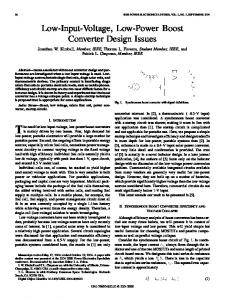
Figure I: Logic diagram of a JK flip-flop from RS flip-flop
to be as low as 2.42nano second while Pavg is as low as 1l.19,..W
14
thereby giving a PDP as low as 2.71 x 10-
Joule for 0.9 volt
power supply. Furthermore there is a remarkable contraction in transistor count compared to conventional synchronously clocked NOR-based transmission
JK
flip-flop
gates
and
comprising CPL,
CMOS
transistors,
accordingly
suggesting
minimization of area. The simulation of the proposed design has been carried out in Tanner SPICE and the layout has been designed in Microwind.
Keywords-Modified Gate Diffusion Input (GDI) procedure, low power, high speed, power delay product (PDP), transistor count, area 1.
INTRODUCTION
The realm of sequential logic systems deems a flip-flop as a crucial and vital component where the output at any instant of time relies on the prevailing input in adjunction with the precedent output. Thus, a flip-flop is also a memory element. Such a memory element composes of combinational logic gates such as NOT, OR, AND, NOR, NAND, CMOS latches, transmission gates, feedback and so on [1]. A JK flip-flop is one of the most important flip-flops as all the other flip-flops viz. RS, D and T can be derived from it. Hence, JK flip-flop is also called a Universal flip-flop. In addition to this, a JK flip flop eliminates the problem of not-allowed input combination which is pronounced in case of a RS flip-flop i.e. the RS flip flop possesses a dilemma with R=S=1 input state by delivering erratic outputs. The JK flip-flop incorporates two feedback lines between the outputs together with the inputs as displayed in fig 1 with the purpose of overcoming the aforesaid predicament. The JK flip-flop holds its present state whilst the clock remaining inactive [2].
978-1-4799-3080-7114/$31.00 ©2014 IEEE
Moreover, a JK flip-flop is used as a counter in sequential circuits and is also utilized in data processors [3]. In topical era, applications are targeted at battery operated appliances so that power dissipation becomes one of the chief design constraints [2]. Earlier processor speed, circuit speed, area, performance, cost and reliability were of crucial significance. Power consumption was of inferior apprehension. However, in modern years power consumption is being given equal attention along with high throughput [2]. The reason for such a changing trend is accredited probably due to the swift escalation in portable with wireless devices which would dissipate lesser power but operate at a towering speed while being adept to calculate complicated functions efficiently. To boot to this, high performance processors consume rigorous power which in turn augments the wrapping and refrigerating cost. Eventually there is an ascent in the power density of VLSI chips thereby agitating the reliability [2], [4]-[10]. It has been ascertained that every 100 levitation in operating temperature nearly doubles the failure rate of constituents made up of Silicon because of varied Silicon breakdown methods for instance thermal runaway, electrical parameter shift , junction diffusion, electromigration diffusion, package related failure as well as Silicon interconnect failure [11]. From the environment point of view, the fewer the power dissipation of electronic components, fewer will be the heat dissipated in rooms which in turn will have an affirmative influence on the global environment. Also, less electricity will be consumed. Accordingly for further optimization of execution of a JK flip-flop in requisites of dissipation of power, delay time and Power Delay Product (PDP), a unique low power, high speed synchronously clocked NOR-based JK flip-flop is being
600
proposed using modified Gate Diffusion Input (GDI) practice. Modified GDI logic is a novel scheme for designing digital circuits consuming low power in scaled technology offering high speed performance and reduced transistor count and hence diminished area. On comparison with a synchronously clocked NOR-based JK flip-flop constructed using the usual CMOS transistors, transmission gates and Complementary Pass-Transistor Logic (CPL) in 45nm process technology, the recommended JK flip-flop exhibited a reduction of 46.73%, 68.74% and 80.46%, respectively in terms of surface area. The prevalent paper is structured as: Section II delivers a brief account of Gate Diffusion Input (GDI) technique whereas section III conveys a short account of Modified Gate Diffusion Input (GDI) approach. Section IV exudes some of the logic gates that can be spawned using modified GDI technique along with a succinct analysis. Section V reveals the JK flip flop that is contemplated for proposition while Section VI imparts the simulation as well as performance study of the insinuated JK flip-flop. The paper culminates in Section VII.
the GDI design more compliant than the proverbial CMOS design. Fig. 3 shows the transient response of a basic GDI cell which is relatively analogous to that of a standard CMOS inverter [14], [15]. This analysis is based on the Shockley model where drain current 10 is represented as depicted below [12]:
gs IDo (�) e (qV lkT) (Vgs � Vth: subthreshold region) k {(Vgs- VtI,) Vds- �) V�s} (Vds Vgs- Vth: linear region) �) k(Vgs- VtJ2 (Vds:::O: Vgs- �h: saturation region)
(2)