Available online at www.sciencedirect.com
ScienceDirect Procedia Technology 17 (2014) 107 – 113
Conference on Electronics, Telecommunications and Computers – CETC 2013
Design of a Power Line Communications Transceiver based on OFDM Edward Mitacc Mezaa*, Jorge Benavides Aspiazua a
Facultad de Ciencias e Ingeniería, Pontificia Universidad Católica del Perú, Av. Universitaria 1801, San Miguel, Lima, LIMA32, Peru
Abstract Power Line Communications (PLC) is a technology that takes advantage of the existing electrical infrastructure to deploy communication networks. This paper proposes an architecture for the physical layer (PHY) of a PLC transceiver based on Orthogonal Frequency Division Multiplexing (OFDM) and inspired in the IEEE 1901 standard for Broadband PLC. The designed system is synthesized on a Xilinx Spartan-6 FPGA device, and supports data rates up to 107 Mbps. © ©2014 2014The TheAuthors. Authors.Published Publishedby byElsevier ElsevierLtd. Ltd.This is an open access article under the CC BY-NC-ND license (http://creativecommons.org/licenses/by-nc-nd/3.0/). Selection and peer-review under responsibility of ISEL – Instituto Superior de Engenharia de Lisboa. Peer-review under responsibility of ISEL – Instituto Superior de Engenharia de Lisboa, Lisbon, PORTUGAL. Keywords: Power Line Communications; Transceiver; OFDM; VHDL; FPGA
1. Introduction In the last decades, the demand for broadband multimedia services has increased substantially, and continues to grow at a rapid pace. This has motivated the development of a wide variety of broadband access technologies. Among them, the PLC technology attracts large attention due to the wide availability of power distribution lines [1] [2], as well as its low deployment cost. However, the major factor that has limited the widespread use of this technology was, before the year 2010, the absence of a global standard accepted by the PLC industry. That year, an important step towards establishing a unique standard for PLC was made with the publication of the IEEE 1901 standard, which is today widely supported
* Corresponding author. Tel.: 51-1-626-2000 ext 4684. E-mail address:
[email protected]
2212-0173 © 2014 The Authors. Published by Elsevier Ltd. This is an open access article under the CC BY-NC-ND license (http://creativecommons.org/licenses/by-nc-nd/3.0/). Peer-review under responsibility of ISEL – Instituto Superior de Engenharia de Lisboa, Lisbon, PORTUGAL. doi:10.1016/j.protcy.2014.10.200
108
Edward Mitacc Meza and Jorge Benavides Aspiazu / Procedia Technology 17 (2014) 107 – 113
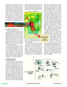
within the industry, mainly because it assures and enhances reliability, security and high-speed in communications over power lines [3][4]. The purpose of this work is to show the design of the physical layer of a PLC transceiver based on the OFDM modulation scheme and inspired in the IEEE 1901 standard. The designed system is fully described using VHDL and synthesized on a Xilinx Spartan-6 FPGA device [5]. In order to verify its performance, the response of the transceiver to power line channel noise models is simulated and analyzed. The rest of the present paper is organized as follows: Section 2 describes the architecture designed, Section 3 shows the synthesis results and the simulations carried out, and finally Section 4 presents the conclusions and future works. 2. PLC transceiver architecture A general block diagram of the proposed PLC transceiver is shown in Fig. 1. This design is based on the processing chain specified on the IEEE 1901 FFT PHY layer model [3] for payload data transmission. At the transmitter, the input data is first scrambled by a pseudo-noise (PN) sequence, in order to avoid long strings of repetitive bits. Next, a rate 1/2 linear convolutional encoder introduces redundant bits, which are used to provide error detection and correction capability. Then, the encoded data is interleaved by a block interleaver to minimize burst errors probability. This is followed by a Quadrature Phase Shift Keying (QPSK) constellation mapping, in which the interleaved data is mapped to QPSK symbols. The serial stream is then converted to a parallel stream that is modulated by means of a 4096-point Inverse Fast Fourier Transform (IFFT) block. The modulated data is converted back to a serial stream, and a cyclic prefix (CP) of 1252 samples is inserted at the beginning of the symbol, in order to avoid inter-symbol interference (ISI) in the case of any delay at the receiver. Finally, the extended symbol is sent to an analog front end (AFE) module which couples the signal to the power line medium. The receiver performs the reverse process carried out at the transmitter. First, the samples corresponding to the cyclic prefix are removed, and then a 4096-point Fast Fourier Transform (FFT) module performs the OFDM demodulation. Next, the data is demapped and de-interleaved, by means of a QPSK demapper module and a block de-interleaver, respectively. This is followed by a convolutional decoding process, which is carried out by a harddecision Viterbi Decoder. This module employs the Viterbi algorithm to determine the most likely transmitted sequence given the received sequence. Finally, the decoded data is de-scrambled by the same PN sequence used at the transmitter.
Fig. 1. Proposed PLC transceiver block diagram.
109
Edward Mitacc Meza and Jorge Benavides Aspiazu / Procedia Technology 17 (2014) 107 – 113
3. Subsystems implementation 3.1. Scrambler The data scrambler block provides the input data a random distribution. Its purpose is to avoid long strings of 1’s and 0’s, which can produce difficulties for synchronization and clock recovery. The input binary stream is scrambled by performing a modulo-2 addition (xor operation) with a pseudo-noise (PN) sequence, which is generated by a linear feedback shift register (LFSR) defined by the following characteristic polynomial:
S ( x) x10 x 3 1
(1)
Fig. 2 shows the implemented data scrambler. The 10-bit LFSR is initialized to all ones at the beginning of each frame.
Fig. 2. Data scrambler.
3.2. Convolutional Encoder The convolutional encoder and Viterbi decoder blocks are used together to provide error correction capability over a noisy channel. The implemented convolutional encoder has a native rate of 1/2, and a constraint length equal to K = 3, as it is shown in Fig. 3a. The corresponding Trellis diagram is illustrated in Fig. 3b, where solid lines denote the state transition driven by input bit 0 and dashed lines denote the transition driven by input bit 1. Annotated on each arrow are the outputs (outputs 1 and 0, respectively) generated by the input given the encoder state. From the figure it can be seen that, after three transitions from the initial state 000, the encoder reaches the steady state, in which the state transition pattern repeats at each time instance.
Fig. 3. (a) Convolutional encoder; (b) Trellis diagram of convolutional encoder.
110
Edward Mitacc Meza and Jorge Benavides Aspiazu / Procedia Technology 17 (2014) 107 – 113
3.3. Interleaver The interleaver block rearranges input data such that consecutive data are spaced apart, and thus minimizes burst errors probability. The implemented block interleaver employs two buffers organized as 1024x4 matrices, which are used to store information bits (output bit 0 in encoder) and parity bits (output bit 1 in encoder). Each buffer is divided into 4 equal sub-blocks of 1024 bits. The interleaving procedure is performed in two steps. First, the two input bits are written into their respective buffers column-wise. The first 1024 information and parity bits are stored in their respective first sub-block, the next 1024 information and parity bits in their respective second sub-block, and so on. This is illustrated in Fig. 4. Then, data is read out of the matrix row-wise, two bits at a time, starting from row one. The first two bits are read out of the row one of the first two sub-blocks, the next two bits are read out of the row one of the next two sub-blocks, and so on.
Fig. 4. Data interleaver.
3.4. QPSK Mapper The QPSK mapper block takes the interleaved data in groups of two bits, and maps them to appropriate QPSK symbols. Table 1 shows how the bits are mapped to in-phase (I) and quadrature (Q) components of a symbol. The implemented mapper consists of a ROM containing the I and Q values, and two multiplexers which select the corresponding output values. Table 1. QPSK symbol mapping Input bits
Mapped values
b1
b2
I
Q
0
0
-1
-1
0
1
-1
+1
1
0
+1
-1
1
1
+1
+1
Edward Mitacc Meza and Jorge Benavides Aspiazu / Procedia Technology 17 (2014) 107 – 113
111
3.5. IFFT/FFT module The 4096-point IFFT module is used to generate the OFDM symbol in the time domain, while the 4096-point FFT module converts the symbol back to the frequency domain. The Xilinx FFT v8.0 LogiCORE IP processor [6] is employed to perform both the IFFT and FFT operations. The pipelined streaming I/O architecture, which implements the Cooley-Tukey radix-2 decimation-in-frequency (DIF) FFT algorithm, is chosen in order to allow continuous data processing of input data. Both IFFT and FFT modules accept 32-bit fixed-point complex data vectors as inputs, and outputs data vectors of the same length in natural order. Phase factor width is configured to 16 bits, and convergent rounding is chosen for the rounding method. 3.6. Cyclic prefix insertion/removal In order to minimize inter-symbol interference (ISI), a cyclic prefix (CP) of 1252 samples is appended at the beginning of the OFDM symbol, before it is sent to the analog front end (AFE) module. At the receiver, these samples corresponding to the CP are discarded before the FFT is computed. 3.7. Viterbi Decoder The Viterbi decoder block generates one bit for each two bits of input. It employs the Viterbi algorithm [7] to find the path in the Trellis diagram whose sequence of output symbols is the closest match to the received data sequence. This block consists of five functional units: branch metric calculation (BMC) units, add-compare select (ACS) units, memory banks, trace-back units (TBUs) and display memories. Fig. 5 illustrates the architecture of the implemented Viterbi decoder. The BMC units calculate the Hamming distance (metric) between the received inputs and the possible ideal inputs at each state transition in the Trellis diagram. The ACS modules compute the accumulated metric associated with each state transition, and select the lowest one as the new metric for each state. The selected state transitions are written in four 16x8 memory banks in round robin manner. Then, TBUs traverse back in the Trellis mesh and identify the decoded outputs. Two parallel working TBUs are used in the design, and thus decoded data is available after tracing back two memory banks. Display memories are employed to store temporarily the decoded outputs.
Fig. 5. Viterbi decoder.
112
Edward Mitacc Meza and Jorge Benavides Aspiazu / Procedia Technology 17 (2014) 107 – 113
4. Synthesis and simulation results The designed system was described using VHDL and synthesized on the Xilinx Spartan-6 XC6SLX45 FPGA device using the Xilinx ISE 14.4 software. Table 2 shows the FPGA logical resources employed. Table 2. Spartan-6 XC6SLX45 logical resources utilization Resources
Transmitter
Receiver
Transceiver
Number of slice registers
6832 (12%)
6495 (11%)
13357 (24%)
Number of slice LUTs
4790 (17%)
4790 (17%)
9576 (35%)
Total number of slices
1778 (26%)
1834 (26%)
3586 (52%)
Maximum operating frequency
122.46 MHz
124.83 MHz
107.68 MHz
The transceiver operates at a maximum frequency of 107.68 MHz, and thus supports data rates up to 107 Mbps. As it is shown, the complete system utilizes 52% of the resources of the FPGA. The most demanding blocks are the IFFT/FFT modules, due to its high hardware complexity. In order to evaluate the bit error rate (BER) performance of the designed transceiver over a noisy channel, the periodic synchronous and periodic asynchronous impulsive noise models presented in [8] are employed, and the receiver response is simulated in each case. The resulting BER plots are shown in Fig. 6.
Fig. 6. (a) BER vs SNR plot for OFDM signal with periodic synchronous impulsive noise; (b) BER vs SNR plot for OFDM signal with periodic asynchronous impulsive noise.
5. Conclusion and Future Works In this paper, an architecture for the physical layer (PHY) of a PLC transceiver based on OFDM was presented. The system, synthesized on a Xilinx Spartan 6 FPGA device, supports data rates up to 107 Mbps. The simulation results verified the correct operation and performance of the transceiver. The system is being completed with the integration of time and frequency synchronization blocks at the receiver, in order to ensure correct frame detection. The design could also be complemented with other works to complete the architecture of a PLC transceiver fully compliant with the IEEE 1901 standard.
Edward Mitacc Meza and Jorge Benavides Aspiazu / Procedia Technology 17 (2014) 107 – 113
References [1] Hendrik C. Ferreira, Lutz Lampe, John Newbury, Theo G. Swart. Power Line Communications: Theory and Applications for Narrowband and Broadband Communications over Power Lines, Wiley, 2010. [2] Medium Access Control for Power Line Communications: An Overview of the IEEE 1901 and ITU-T G.hn Standards, IEEE Communications Magazine, pp. 183-191, June 2011. [3] IEEE Standard for Broadband over Power Line Networks: Medium Access Control and Physical Layer Specifications, IEEE Std 1901-2010. [4] IEEE 1901 Access System: An Overview of Its Uniqueness and Motivation, IEEE Communications Magazine, pp. 150-157, October 2010. [5] Xilinx. Xilinx DS160 Spartan-6 FPGA Family Data Sheet, Xilinx Corporation, 2011. [6] Xilinx. Xilinx LogiCORE IP Fast Fourier Transform v8.0 Data sheet, Xilinx Corporation, 2012. [7] A. J. Viterbi, J. K. Omura. Principles of Digital Communication and Coding. McGraw-Hill, 1979, pp. 258-261. [8] Working Group on Power Line Communications, Communications Engineering Department, University of Málaga. Online: [cit. 2013-11-15].
113