and the design of all-digital I&Q demodulators is cov- .... sign. The restriction on fs to be a minimum of twice the Nyquist frequency arises in order to avoid overlap ...
16th European Signal Processing Conference (EUSIPCO 2008), Lausanne, Switzerland, August 25-29, 2008, copyright by EURASIP
DIGITAL I&Q DEMODULATION IN ARRAY PROCESSING: THEORY AND IMPLEMENTATION David Bernal, Pau Closas, Juan A. Fern´andez–Rubio Dept. of Signal Theory and Communications, Universitat Polit`ecnica de Catalunya (UPC) Jordi Girona 1-3, Campus Nord, 08034 Barcelona, Spain. e-mail: {bernal,closas,juan}@gps.tsc.upc.edu http://gps-tsc.upc.es/comm
ABSTRACT Following the IF sampling strategy, a receiver is able to overcome inherent limitations of conventional I&Q demodulators, performing this operation in a completely digital manner. In this paper, IF sampling is analyzed both from theoretical and implementation points of view for the case of an antenna array based receiver. Both analysis are complementary and provide useful guidelines for the design of Software-Defined Radio receivers. The foundations of IF sampling strategy are presented and the design of all-digital I&Q demodulators is covered. Finally, an application to the design of a S-DMB receiver is also presented and FPGA implementation issues discussed. 1. INTRODUCTION In communication systems, a signal is baseband modulated in its in–phase (I) and quadrature (Q) components, which are transmitted to the Radio Frequency (RF) spectrum. Receivers are in charge of demodulating the I&Q components of the received signal. A conventional I&Q demodulator is shown in Figure 1. Basically, it consists in splitting the received signal and multiplying each arm by a local oscillator (LO) and its 90o shifted version. This procedure provides I&Q components after lowpass filtering and quantization. A number of errors may appear when considering the conventional approach shown in Figure 1, mainly caused because the two arms must be closely matched for correct demodulation, e.g. gain balance, quadrature-phase balance or DC offsets. New trends following the Software-Defined Radio (SDR) philosophy emerged [1, 2], mainly thanks to recent advances in high-speed analog-to-digital converters (ADC), that allow IF sampling strategies to be envisaged and the I&Q demodulator to be implemented digitally, overcoming some of the aforementioned errors [3]. Certainly, the analog components of the RF/IF chain have to be still carefully designed. However, a direct downconversion might be unaffordable in highspeed applications [4]. This paper presents both theoretical and implementation aspects of IF sampling, focusing on the demodulation of I&Q components in a completely digital fashion. Section 2 provides a detailed overview of IF sampling strategies and the signal processing involved. Although This work has been financed by the Spanish/Catalan Science and Technology Commissions and FEDER funds from the European Commission: TEC2006-06481/TCM, TEC2004-04526, TIC2003-05482 and 2005SGR-00639.
Figure 1: Conventional I&Q demodulator. this is an increasingly used technique in SDR receivers [5], this paper presents useful design guidelines. In addition, the case of an antenna array receiver is addressed, where the use of Matched Filters may not be possible due to area constraints in the digital platform. The latter introduces a spurious interference, whose impact is discussed from an array processing point of view. Section 3 is devoted to the implementation concerns of digital I&Q demodulation. Finally, Section 4 presents an application to the design of a S-DMB receiver [6] in the S-band. The resulting design has been programmed in VHDL code and implemented in an FPGA device, some results are discussed. 2. DIGITAL I&Q DEMODULATION: THEORY A complex baseband signal b(t), that has a bandwidth of B Hz, is transmitted at RF. We define bI (t) and bQ (t) as the in-phase and quadrature components of b(t). After downconversion to an Intermediate Frequency, fIF , the signal is bandpass filtered at the receiver to avoid aliasing and to remove high-frequency components. Thus, at the output of the RF chain, the received real signal consists of the desired IF signal corrupted by noise: xIF (t) = a V (t) cos (2πfIF t + Θ(t)) + ν(t)
(1)
where a is the amplitude of the signal and ν(t) is additive noise. V (t) and Θ(t) are the envelope and the phase of b(t) = bI (t) + jbQ (t), respectively. The IF signal feds an ADC which samples signal at a sampling rate of fs = 1/Ts with nb bits of quantization. Hence, the sampled version of the IF signal can be expressed as: xIF [n] = a V [n] cos (2πfIF nTs + Θ[n]) + ν[n]
(2)
16th European Signal Processing Conference (EUSIPCO 2008), Lausanne, Switzerland, August 25-29, 2008, copyright by EURASIP
The idea behind digital IF sampling is to undersample IF signal in order to obtain a replica of the signal at baseband, without requiring an additional downconversion. This can be accomplished by properly choosing fIF and fs . In general, the following relations fIF fs
= kfs ± ≥ 4B
fs 4
¯ , ∀k ∈ Z ¯ k ≥ 1 (3)
ensure that a non-overlapped alias will appear centered at fs /4. Then, one of the replicas at ±fs /4 can be downconverted to baseband using the frequency-shifting property of the Fourier transform of a signal, i.e., Z(f ± F fo ) ↔ z[n]e∓j2πfo nTs . With fo = fs /4, it results that π we have to multiply the IF signal by e−j 2 n to shift the spectrum to the left. Actually, this is a straightforward π operation since the sequence of cyclic values of e−j 2 n 2 are {1, −j, −1, j}, where j = −1. As shown in Figure 2, this provides the I and Q components of the desired signal.
Figure 3: Up-down: spectral densities of xIF (t), xIF [n] π and x[n] = xIF [n] · e−j 2 n . along the array as much smaller than its inverse bandwidth, a phase shift can be used to describe the propagation from one antenna to another. Hence, it can be assumed that the signal waveform is identical in each element of the antenna array for a given instant. For the i–th antenna element, the single snapshot signal model for an arbitrary antenna array geometry is given by
Figure 2: After frequency-shift, I&Q components are obtained. Figure 3 shows the spectra of the signals involved in the process. SIF (f ) is the spectral density of the received IF signal in equation (1). Setting fIF = 3fs /4, i.e. k = 1, and sampling xIF (t) according to equation (3), we can observe in Figure 3 that aliasing appears adc without overlapping in its spectrum SIF (f ) - recalling that we have assumed a band-limited signal V [n]. After frequency-shift, we obtain a baseband replica of the adc desired signal in S(f ) = SIF (f − fs /4). adc Notice that the spectral density SIF (f ) shown in Figure 3 is obtained for any chosen k in (3). Thus, the selection of k is related to implementation issues, i.e., to select a suitable fIF for the application under design. The restriction on fs to be a minimum of twice the Nyquist frequency arises in order to avoid overlapadc ping in SIF (f ). After lowpass filtering S(f ) one can decimate the signal up to a factor that depends on the chosen sampling frequency. Now we consider the case of an antenna array based receiver and provide a detailed analysis of the digital signal processing involved in the digital I&Q demodulation procedure. In an N element antenna array, each antenna element receives a different replica of signal in (1), with a different gain and phase depending on the array geometry and the Directions Of Arrival (DOA) [7, 8]. Assuming the narrowband array assumption, consisting of taking the time required for the signal to propagate
xiIF [n] = gi a V [n] cos (2πfIF nTs + Θ[n] − γi ) + ν i [n] (4) where gi and γi are the gain and phase of the i–th antenna element respectively. ν i [n] is the additive noise contribution to xiIF [n]. Setting hereafter fIF = 3fs /4 for the sake of clarity, we can express the snapshot model as: µ ¶ 3π xiIF [n] = gi a V [n] cos n + Θi [n] + ν i [n] (5) 2 where Θi [n] , Θ[n] − γi . The cosine can be expanded as µ ¶ 3π n + Θi [n] = (6) cos 2 µ ¶ µ ¶ ¡ ¢ ¡ ¢ 3π 3π cos n cos Θi [n] − sin n sin Θi [n] , 2 2 with the sequences of cyclic values with n: µ ¶ 3π 1 n cos n = j (1 + (−1)n ) ∈ {1, 0, −1, 0} (7) 2 2 µ ¶ 3π 1 sin n = − j n+1 (1 − (−1)n ) ∈ {0, −1, 0, 1} 2 2 When multiplying xiIF [n] by the complex exponenπ tial e−j 2 n we obtain that the I&Q components of the resulting signal are: ¡ ¢ a xiI [n] = gi V [n] cos Θi [n] (1 + (−1)n ) + ν˜Ii [n] 2 ¡ ¢ a i xiQ [n] = gi V [n] sin Θi [n] (1 − (−1)n ) + ν˜Q [n] (8) 2
16th European Signal Processing Conference (EUSIPCO 2008), Lausanne, Switzerland, August 25-29, 2008, copyright by EURASIP
being ν˜Ii [n] and ν˜Ii [n] the I&Q components of the reπ sulting noise, ν˜i [n] = ν i [n] · e−j 2 n . Then, the complex baseband signal can be expressed, for each antenna element, as
Apart from avoiding the above cited inherent errors of conventional approaches, some particularities of an all-digital I&Q demodulator are of interest when addressing its implementation. Comparing the diagrams of a conventional and an xi [n] = xiI [n] + jxiQ [n] (9) all-digital I&Q demodulator, Figures 1 and 4 respech i i tively, it arises that the number of input pins to the digi a = gi V [n] ejΘ [n] + (−1)n e−jΘ [n] + ν˜i [n] ital platform has been reduced to a half since only the 2 sampled real IF signal is required - considering that the a a = b[n] gi e−jγi + b∗ [n] (−1)n gi ejγi + ν˜i [n] digital platform is located after ADCs in both schemes. 2 2 Thus, for an N element array where the ADC samples at fs and quantizes with nb bits in parallel we would Arranging signals from elements in row vectors, baserequire N · nb inputs to perform digital I&Q demodulaband signal in (9) can be expressed as tion, instead of the 2·N ·nb delivered in the conventional a a ∗ approach. n ∗ x[n] = b[n] sd + b [n] (−1) sd + n[n] (10) 2 2 where £ ¤T • x[n] = x1 [n], . . . , xN [n] ∈ CN ×1 is the signal vector whose rows corresponds to each antenna IFsampled output. £ ¤T • sd = g1 e−jγ1 , . . . , gN e−jγN ∈ CN ×1 is the steering vector of the signal, i.e., a row vector containing the response of the elements to the direction of the signal. £ ¤T • n(t) = ν˜1 [n], . . . , ν˜N [n] ∈ CN ×1 represents additive noise and all other disturbing terms. The spectral contribution of the two signal terms in equation (10) can be observed in Figure 3, for the case of a single antenna sd = 1. The first term corresponds to the desired baseband signal, b[n]. The second term, b∗ [n](−1)n , corresponds to replicas centered at ±fs /2, being uncorrelated with b[n]. As shown in Figure 3, x[n] can be low-pass filtered with two Matched Filters (I&Q) in order to recover b[n] reducing the contribution of b∗ [n](−1)n . However, when considering an antenna array, it could happen that the use of 2 · N Matched Filters in parallel requires an unaffordable computational cost and that matched filtering must be performed at the output of the antenna array, after beamforming. In that case, it is seen from equation (10) that, in addition to the desired signal, an interference is caused by b∗ [n](−1)n being its steering vector the complex conjugate of sd . Particularizing for the case of a planar array, it is straightforward to observe that the conjugate of sd corresponds to the steering vector of the specular multipath of b(t). Thus, if beamforming is performed, the computed weights according to any optimal criteria will attempt to null the direction where the fictitious specular replica appears. For the case of a conformal array, it is not apparent that s∗d represents an actual steering vector.
Figure 4: Digital IF sampling with I&Q demodulation. As could be devised from Figure 2, the implemenπ tation of xIF [n] · ej 2 n is straightforward in an FPGA. This process only requires to split into two arms even and odd samples and then, multiply each arm with a cyclic sequence of ±1 values. The latter operation is performed at fs /2, since null-values in-between do not need to be multiplied. The proposed architecture is shown in Figure 5, along with the operating function at each point. Actually, the product by ±1 does not requires a multiplier, as only the two’s complement is performed when multiplying by −1 and a bypass for the case of 1, saving computational resources. Additionally, one can decimate each arm in order to remove the null-values. This decimation will reduce the operating frequency of the FPGA to fs /2, since the block in Figure 5 is located immediately after signal has been delivered to the FPGA. This can be performed at the expenses of more laborious designs. This is of interest in high-frequency applications, where FPGAs do not operate efficiently, reducing the operating frequency.
3. DIGITAL I&Q DEMODULATION: FPGA IMPLEMENTATION Due to the inherent nature of the parallel processing in an antenna array receiver, it is apparent that an FPGA device is a proper platform. In addition, this platform provides high degrees of reconfigurability, following the SDR philosophy.
π
Figure 5: Implementation of the e−j 2 n product at the i-th array element.
16th European Signal Processing Conference (EUSIPCO 2008), Lausanne, Switzerland, August 25-29, 2008, copyright by EURASIP
4. APPLICATION TO THE S-DMB STANDARD The general concepts presented along Sections 2 and 3 have been applied to the design of an antenna array based S-DMB receiver under the SDR paradigm for Sband operation. S-DMB is designed to provide satellite and complementary terrestrial on–channel repeater services for high–quality audio and multimedia data for vehicular, portable and fixed reception [6]. The main characteristics of the system are now presented (those which are of interest for the design of the digital I&Q demodulator). A satellite transmits 30 channels multiplexed using CDMA on QPSK modulation at fRF = 2642.5 MHz. The chip rate is rc = 16.384 MHz, the processing gain 64 and the transmitted signal is filtered by a square–root raised cosine with a roll-off factor ρ = 0.22. Due to acquisition and tracking issues it is desirable to have at least 4 samples per chip, for this reason it has been set fs = 4rc = 65.536 MHz, nb = 8 bits and, according to equation (3) with k = 1, fIF = 49.152 MHz. Notice that with this design we ensure the condition in equation (3), B = (1 + ρ) r2c ≤ 4fs . An antenna array receiver (N = 40) has been designed, being the digital platform programmed in VHDL code and synthesized into a Xilinx FPGA device. Beamforming with antenna arrays consists of several antennas, whose outputs are controlled in phase and gain, i.e., multiplied by complex weights, in order to achieve a gain pattern that can be manipulated electronically. Then, all the weighted signals are combined to obtain a single output y[n]. These mentioned weights can be stacked in T a complex–valued vector w ∈ CN ×1 = [w0 , · · · , wN −1 ] , and the output signal of the beamformer can be computed as y[n] = wH x[n]. Weight vector w can be designed following several criteria, usually exploiting the spatial filtering provided by antenna arrays. Since the aim of the present paper is to study digital I&Q demodulation, we now emphasize on this subsystem of the whole receiver presented in [9]. For the sake of clarity, Figure 6 presents the block diagram of the Digital Beamforming receiver and the location of the digital I&Q demodulation block in it, which consists in a bank of N I&Q demodulators in parallel, similar to that shown in Figure 5. Notice that, for this application, the IF sampling strategy results especially helpful as it reduces the number of signal input pins to the FPGA from 640 to 320, apart from avoiding errors of conventional I&Q demodulators. The schematic description of the digital I&Q demodulator is shown in Figure 7. Other attempts to implement digital I&Q demodulators can be found in the literature [5, 10, 11, 12] for other communication systems. Nevertheless, the schematic in Figure 7 has been designed taking into account the S-DMB specifications. Therefore, there are some remarkable particularities w.r.t. the generic block presented in Figure 5. Since we have considered 4 samples per chip, the implemented block for the S-DMB receiver is composed of four parallel blocks, corresponding to each sample. Hence, we have replaced the multiplexer and the two multipliers in Figure 5 by 4 different blocks, being two arms created for each component, one for those samples multiplied
Figure 6: Digital Beamforming receiver with digital I&Q demodulation.
Figure 7: Schematic of the implemented digital I&Q demodulator. by −1 and another for those bypassed, operating at a frequency of fs /4. In general, one can increase the granularity of the design in order to decrease the operating frequency (ff pga ) at the expenses of increasing the consumed area (Af pga ) in the FPGA, since more blocks are required. As a rule of thumb, it is considered that the following holds ff pga · Af pga = κ, where κ is a constant, i.e. the product defines an hyperbolic behavior. Table 1 shows Af pga and ff pga synthesis results of schematic in Figure 7 for a number of Xilinx FPGA devices. It is remarkable that not only the number of inputs are reduced, but also little computational cost is introduced by the digital I&Q demodulator w.r.t. direct downconversion strategies. Technology XC5VLX220 XC4VLX200 XC3S1600E XC3S4000L
Af pga (Slices) 48 of 138240 37 of 89088 37 of 14752 37 of 27648
ff pga (MHz) 603.136 522.193 295.513 223.364
Table 1: Synthesis results of the I&Q demodulation block into different Xilinx F P GA technologies.
16th European Signal Processing Conference (EUSIPCO 2008), Lausanne, Switzerland, August 25-29, 2008, copyright by EURASIP
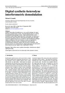
ital signal processing device and allows high degrees of downconversion configurations. A generic block diagram has been presented, which is a straightforward implementation of the digital I&Q demodulator. As an example, it has been presented an application of those concepts to the design of a S-DMB antenna array receiver, which has been programmed in VHDL code and implemented on an FPGA device, validating the above discussions. REFERENCES Figure 8: Correlator output without Matched Filtering after digital I&Q demodulation.
Figure 9: Radiation Pattern after Digital Beamforming: desired signal at 0o and a jammer at 9o . Finally, to assess the correct operation of the tested digital demodulation block, some results of the overall SDMB receiver [9] are presented. In particular: synchronism acquisition via code correlation and pattern computation. On the one hand, Figure 8 shows the correlator output when no matched filtering is applied to the digitally demodulated I&Q components. Notice that the interference in equation (10) does not significantly affect the performance since the factor (−1)n uncorrelates this signal with the generated local CDMA code. On the other hand, the Digital Beamforming technique, namely the Temporal Reference Beamforming beamformer [8], has been implemented after digital I&Q demodulation. Basically, it uses the well-known waveform structure of a transmitted pilot signal to point the beam of the antenna array. Figure 9 shows the computed beampattern for a S-DMB signal at 0o and a jammer at 9o . It is readily seen that the Digital Beamforming module is correctly operating, being the jammer nulled and the desired signal pointed. 5. CONCLUSIONS IF sampling has emerged as a feasible and appealing strategy for SDR receivers. In this paper, a theoretical analysis has been provided along with design guidelines and the digital I&Q demodulator studied for a general antenna array receiver. In addition FPGA implementation issues were discussed, concluding that digital I&Q demodulation reduces the number of inputs to a dig-
[1] J. Mitola, Software Radio Architecture: ObjectOriented Approaches to Wireless Systems Engineering, Wiley Interscience, 2000. [2] Jeffrey H. Reed, Software Radio: A Modern Approach to Radio Engineering, Prentice Hall, 2002. [3] J. Tsui, Digital Techniques for Wideband Receivers, Artech House, Norwood, 2 edition, 2001. [4] R. H. Walden, “Analog-to-Digital Converter Survey and Analysis,” IEEE J. Select. Areas Commun., vol. 17, no. 4, pp. 539–550, April 1999. [5] H. Samueli and B. C. Wong, “A VLSI Architecture for a High–Speed All-Digital Quadrature Modulator and Demodulator for Digital Radio Application,” IEEE J. Select. Areas Commun., vol. 53, no. 8, pp. 1512–1519, October 1990. [6] “ITU-R BO.1130-4: Systems for digital satellite broadcasting to vehicular, portable and fixed receivers in the bands allocated to BSS (sound) in the frequency range 1 400–2700 MHz,” Tech. Rep., International Telecommunications Union - Radiocommunications (ITU-R), 2001. [7] Robert A. Monzingo and Thomas W. Miller, Introduction to Adaptive Arrays, John Wiley & Sons, 1980. [8] Harry L. Van Trees, Optimum Array Processing. Detection, Estimation and Modulation Theory, Part IV, Wiley Interscience, 2002. [9] O. L¨ ucke, A. Pellon, P. Closas, and J. A. Fern´andezRubio, “Cost-optimised active receive array antenna for mobile satellite terminals,” in IST Mobile Communications Summit 2007, Budapest, Hungary, July 2007. [10] B.E. Priyanto, C.L. Law, and Y.L. Guan, “Design & implementation of all digital I-Q modulator and demodulator for high speed WLAN in FPGA,” in Proceedings of the IEEE Pacific Rim Conference on Communications, Computers and signal Processing, PACRIM 2003, August 2003, vol. 2, pp. 659–662. [11] C.C. Jong, Y.Y.H. Lam, and L.S. Ng, “FPGA implementation of a digital IQ demodulator using VHDL,” in Proceedings of the 7th International Workshop on Field-Programmable Logic and Applications, FPL 1997, pp. 410–417. [12] S.S Abeysekera and C. Charoensak, “FPGA implementation of a Σ − ∆ architecture based digital IF stage for software radio,” in Proceedings of the 15th Annual IEEE International, ASIC/SOC Conference, 2002, September 2002, pp. 341–345.