Mailing Address: PO Box 11400 ⢠Tucson, AZ 85734 ⢠Street Address: 6730 S. ... Aux Amp. Out. 12. High-Pass. Out. Band-Pass. Out. Low-Pass. Out. Notch .... right of TI covering or relating to any combination, machine, or process in which such.
APPLICATION BULLETIN
®
Mailing Address: PO Box 11400 • Tucson, AZ 85734 • Street Address: 6730 S. Tucson Blvd. • Tucson, AZ 85706 Tel: (602) 746-1111 • Twx: 910-952-111 • Telex: 066-6491 • FAX (602) 889-1510 • Immediate Product Info: (800) 548-6132
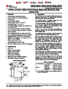
DIGITALLY PROGRAMMABLE, TIME-CONTINUOUS ACTIVE FILTER by Johnnie Molina, (602) 746-7592
Programmable active filters have increased in popularity over the past decade. With the advent of switched capacitor topologies, filter parameters such as the natural frequency and filter Q can be changed simply by varying the clock frequency. But switched capacitor filters are sampled data systems and are subject to anomalies such as clock feedthrough noise and aliasing errors.
Digital Word In
The circuit in Figure 1 shows how an analog, digitally programmable filter can be built using a UAF42. This monolithic, state-variable active filter chip provides a two pole filter building block with low sensitivity to external component variations. It eliminates aliasing errors and clock feedthrough noise common to switched capacitor filters. Lowpass, highpass, bandpass and notch (band reject) outputs are available simultaneously.
D1 - D12
Pins 4
Pins 15
18
4
15
18
OPA627 17
OPA627 17
1
DAC7541A 2
1
DAC7541A 2
RF1 13kΩ
RF2 13kΩ
10kΩ RQ 35.4kΩ
10kΩ 13
8
7
14
5
50kΩ
RG 49.9kΩ
UAF42
C1
C2
1000pF
1000pF
50kΩ
10kΩ
1
In 12
Aux Amp Out 6
50kΩ
50kΩ
(NC) 2
3
(13)
9 V–
High-Pass Out
10
(7)
11
(1)
4
V+
Band-Pass Out
Low-Pass Out
Notch Out
FIGURE 1. Digitally Programmable Analog Filter.
©
SBFA005
1994 Burr-Brown Corporation
AB-062
Printed in U.S.A. February, 1994
The circuit uses the UAF42 state-variable filter IC, two op amps, a few resistors and two common MDACs. Capacitors aren’t required because the UAF42 has on chip 1000pF, 0.5% precision capacitors. The MDACs function as voltage attenuators which influence the unity-gain bandwidth of the integrators on board the UAF42. The filter’s natural frequency, fO, is described by the following relationships:
f O = DAC GAIN • f OMAX DAC GAIN =
f OMAX =
HIGHPASS OUT 3
0
(1) Gain (dB)
Where:
The highpass, bandpass and lowpass outputs yield the responses shown in Figure 3.
X 2n
1 2 • π •10 –9 • R F
R F = R F1 = R F2
–3
–6
and, –9
X = digital word at DAC inputs D1 – D12
1
10
100
1000
f–3dB = 60Hz
n = number DAC bits BUILD A NOTCH FILTER For example, to program a 60Hz notch filter with the circuit shown in Figure 1, the digital word to the MDAC is given using Equation 1,
LOWPASS OUT 3
X = 6.28 • 10–9 • RF • fO • 2n
0 Gain (dB)
Given that, fO = 60 RF = 13kΩ n = 12
–3
then, X = 20.1
–6
The 12-bit digital word to the DAC should be 20 or 000000010100. The rounding error introduced is 0.3% (fNOTCH = 59.8Hz). Note that the natural frequency, fO, is equal to fNOTCH.
–9 1
10
100
1000
f–3dB = 60Hz
Figure 2 shows the response seen at the band reject or “Notch Out” node. BANDPASS OUT 0
NOTCH OUT 0 –3
Gain (dB)
Gain (dB)
–10
–20
–30
–6
–9
–40 –12 1
–50 1
10
100
10
100
1000
fCENTER = 60Hz
1000
fNOTCH = 60Hz
FIGURE 2. 60Hz Notch Response.
FIGURE 3. Highpass, Lowpass and Bandpass fO = 60Hz Response. 2
fO accuracy can decrease as the DAC gain decreases in an attempt to program low natural frequencies. For example, for a 12-bit DAC and maximum fO set to 20kHz, the resolution giving one LSB change is,
The filter in Figure 1 is set for a Q of 0.707. This can be adjusted using Equation 2 where, RQ = 50kΩ • Q
(2)
Setting the filter to a Q of 0.707 produces second-order Butterworth responses. The Q is not affected by the natural frequency programmed by the DACs. Note that for Butterworth filters, the natural frequency is also the –3dB (half power point) for lowpass and highpass responses. It also is the center frequency for bandpass filters and the notch frequency for band reject responses. The passband gain is unity for all response types except the bandpass. For the bandpass output, the gain at fCENTER is equal to the filter Q.
Resolution =
1 1 • f OMAX = • 20kHz = 4. 9Hz 4096 212
When trying to program low natural frequencies like 12Hz, the digital word to the DAC would be 2. So,
fO =
LIMITATIONS The maximum fO in Figure 1 is set for 12.25kHz. This can be adjusted using Equation 1. Set the DAC gain term equal to (2n – 1)/2n, fO = desired maximum natural frequency and solve for RF.
2 2 • f OMAX = • 20kHz = 9.8Hz 4096 4096
This is an 18% error. Resolution can be increased by reducing fOMAX or using a higher order DAC. RF resistor tolerance should be kept below 1% to maintain fO error to within ±1%.
For example, to extend the maximum fO to 20kHz,
The OPA627 op amps are chosen for their low offset voltage, low noise, low input bias current (FET input), and high unity gain bandwidth (GBW = 16MHz) to maintain stability.
4095 4096 RF = = 7. 96kΩ 2 • π •10 –9 • 20kHz The maximum natural frequency obtainable for the UAF42 is 100kHz.
The information provided herein is believed to be reliable; however, BURR-BROWN assumes no responsibility for inaccuracies or omissions. BURR-BROWN assumes no responsibility for the use of this information, and all use of such information shall be entirely at the user’s own risk. Prices and specifications are subject to change without notice. No patent rights or licenses to any of the circuits described herein are implied or granted to any third party. BURR-BROWN does not authorize or warrant any BURR-BROWN product for use in life support devices and/or systems.
3
IMPORTANT NOTICE Texas Instruments and its subsidiaries (TI) reserve the right to make changes to their products or to discontinue any product or service without notice, and advise customers to obtain the latest version of relevant information to verify, before placing orders, that information being relied on is current and complete. All products are sold subject to the terms and conditions of sale supplied at the time of order acknowledgment, including those pertaining to warranty, patent infringement, and limitation of liability. TI warrants performance of its semiconductor products to the specifications applicable at the time of sale in accordance with TI’s standard warranty. Testing and other quality control techniques are utilized to the extent TI deems necessary to support this warranty. Specific testing of all parameters of each device is not necessarily performed, except those mandated by government requirements. Customers are responsible for their applications using TI components. In order to minimize risks associated with the customer’s applications, adequate design and operating safeguards must be provided by the customer to minimize inherent or procedural hazards. TI assumes no liability for applications assistance or customer product design. TI does not warrant or represent that any license, either express or implied, is granted under any patent right, copyright, mask work right, or other intellectual property right of TI covering or relating to any combination, machine, or process in which such semiconductor products or services might be or are used. TI’s publication of information regarding any third party’s products or services does not constitute TI’s approval, warranty or endorsement thereof.
Copyright 2000, Texas Instruments Incorporated