PHYSICAL REVIEW B 78, 033202 共2008兲
Divacancy clustering in neutron-irradiated and annealed n-type germanium K. Kuitunen,* F. Tuomisto, and J. Slotte Department of Engineering Physics, Helsinki University of Technology, P.O. Box 1100, FI-02015 HUT, Finland
I. Capan Rudjer Boskovic Institute, Zagreb 10 000, Croatia 共Received 12 March 2008; published 8 July 2008兲 We have studied the annealing of vacancy defects in neutron-irradiated germanium. After irradiation, the Sb-doped samples 关共Sb兲 = 1.5⫻ 1015 cm−3兴 were annealed at 473, 673, and 773 K for 30 min. The positron lifetime was measured as a function of temperature 共30–295 K兲. A lifetime component of 330 ps with no temperature dependence is observed in as-irradiated samples, identified as the positron lifetime in a neutral divacancy and indicating that the divacancy is stable at room temperature 共RT兲. Annealing at 673 K resulted in an increase in the average positron lifetime, and in addition, the annealed samples further showed a larger lifetime component of 430 ps at RT, which is due to larger vacancy clusters. The average positron lifetime in the samples annealed at 473 K has a definite temperature dependence, suggesting that the divacancies become negative as the crystal recovers and the Fermi level moves upwards in the band gap. Annealing at 673 K, reduces the average lifetime and intensity of the defect component 2 at RT, indicating that the vacancy clusters have started to anneal. Negative divacancies are still present in the samples after this anneal. Annealing at 773 K is enough to remove all observable vacancy defects. DOI: 10.1103/PhysRevB.78.033202
PACS number共s兲: 78.70.Bj, 61.72.J⫺
I. INTRODUCTION
Germanium as an elemental semiconductor has been shadowed by silicon, when it comes to the use of semiconductor materials in integrated circuits and devices. The supreme properties of silicon include a larger band gap, a stable oxide, and an extremely low surface-state density.1,2 However, electron and hole mobilities are much higher in germanium than in silicon, which has lead to the use of strained Si1−xGex heterostructures to increase mobility in modern transistors.3–5 Even higher charge carrier mobilities could be pursued if transistors were built out of germanium, which is something that is attempted by many groups.6 Even though the history of germanium as a material for semiconductor devices is over 50 years old, very little is known about its material properties, e.g., very few irradiation-induced defects such as vacancies and vacancy impurity complexes have been identified in germanium. Gaining knowledge on the formation, migration, and annealing properties of vacancy defects in germanium is therefore of utmost importance. The apparent low formation energies of vacancy defects in germanium make them suitable agents for, e.g., self-diffusion and diffusion of impurities.7 Also knowledge of the annealing behavior of different defects is very much needed. The investigations of irradiation-induced defects in Ge have been carried out using different techniques, e.g., deeplevel transient spectroscopy 共DLTS兲, Hall measurements, and infrared absorption spectroscopy. Fage–Pedersen et al.8 reported on energy levels of several majority and one minority carrier traps in irradiated Ge. Vanmeerbeek et al.9,10 have used local vibrational mode spectroscopy to study oxygenrelated defects in irradiated and annealed Ge. Computational studies on vacancy defects in germanium have recently been carried out by Coutinho et al.,11 who studied deep carrier traps in a divacancy, and by Janke et al.,12 who made calcu1098-0121/2008/78共3兲/033202共4兲
lations concerning the thermal stability of the divacancy in germanium. The calculations by Janke et al. suggest that most divacancies anneal by migration to trapping centers. Peaker et al.13 have used multiple experimental techniques to study ion-implanted Ge. They propose that the vacancy and interstitial clustering are important mechanisms in implanted germanium. Positron annihilation spectroscopy 共PAS兲 has been established as a versatile tool for studying open volume defects in semiconductors.14 However, as with other techniques, very little work has been published on germanium. Early work from the 1960s on single-crystal Ge include pioneering works by Fabri et al.15 and Fieschi et al.16 However, it is difficult to relate to these studies due to the poor time resolution available in the early days of PAS, which makes comparison between lifetime components questionable. Among the first annealing studies on 共neutron兲 irradiated Ge were Yeh et al.17 and Arifov and Arutyunov.18 It seems that the as-grown samples used in both studies contain native defects, since the average lifetime calculated from the reported annihilation rates 共 = 4.17⫻ 109 s−1兲 is around 240 ps, i.e., approximately 15–20 ps above the bulk lifetime in Refs. 14 and 19 and in the present study. Yeh et al. observed that the trapping rate in as-irradiated samples saturate at 3.32⫻ 109 s−1 after an irradiation fluence of 7 ⫻ 1015 cm−2, corresponding to a lifetime of 301 ps. Similar results were observed by Arifov and Arutyunov after a 2 ⫻ 1018 cm−2 irradiation. Both studies17,18 report that the annealing of the irradiation-induced defects is divided into two steps. The first one at around 573 K apparently results in the formation of larger vacancy clusters. Open volume defects of monovacancy size, with positron lifetimes varying from 278–292 ps have been reported by Moser et al.,20 Corbel et al.21 and Wurschum et al.19 More recently, Polity et al.22 have studied the formation and annealing of Frenkel pairs and vacancyoxygen pairs in electron-irradiated Ge with positrons. Va-
033202-1
©2008 The American Physical Society
PHYSICAL REVIEW B 78, 033202 共2008兲
BRIEF REPORTS
cancy clustering and the annealing of these clusters have been studied by Krause–Rehberg et al.23 Similar results in self- and Si-implanted Ge have been reported by Peaker et al.13 Recrystallization of ion-implanted amorphous Ge have been studied with PAS by Slotte et al.24 In this Brief Report, we have studied neutron-irradiated Ge samples doped with Sb with positron lifetime spectroscopy. We show that irradiation generates vacancy defects that tentatively are identified as divacancies. At the annealing temperature of 473 K, the majority of the vacancy defects turns mobile and form bigger vacancy clusters. However, temperature dependence in the defect lifetime component shows that some defects of divacancy size that are in a negative charge state are stable after annealing at 473 K. Annealing at 673 K removes most of the clusters and also a considerable fraction of negatively charged vacancy defects of divacancy size. An annealing temperature of 773 K is required to remove these defects.
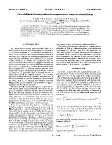
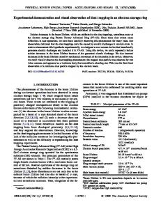
80
a)
I2 (%)
60 40 20
480
b)
No annealing Ann. at 473 K Ann. at 673 K Ann. at 773 K
τ2 (ps)
440 400 360 320
II. EXPERIMENTAL DETAILS
III. RESULTS
We have carried out positron lifetime experiments as a function of temperature and the results for the as-irradiated and annealed samples are shown in Fig. 1.
340
c)
τave (ps)
320 300 280 260 240 220 300 280
d)
260 τ1 (ps)
The measured samples were n-type Ge 共110兲 bulk crystals, in which the dopant Sb concentration was 1.5⫻ 1015 cm−3. The samples were irradiated with fast neutrons up to a fluence of approximately 1016 cm−2 and annealed in 473, 673, and 773 K. We used a conventional fast-fast coincidence system with a resolution of 260 ps and a 20 Ci 22NaCl source to measure positron lifetime spectra. The reference 共bulk兲 lifetime in the measurements was B = 224 ps. Prior to the analysis, the positron annihilations in the source material and in the Al foil covering the source, as well as positronium annihilations as positronium and in the reference sample, were subtracted from the lifetime spectra. The sample temperature during the measurements was controlled by a closed-cycle He cryostat with resistive heating. The lifetime spectra n共t兲 = 兺iIi exp共−t / i兲 were analyzed in terms of exponential decay components convoluted with the Gaussian resolution function of the spectrometer. The indexes i correspond to the different lifetime components in the spectra with individual lifetimes i and intensities Ii. The increase of the average positron lifetime ave = 兺iIii above the bulk lifetime is a signal of vacancy defects being present in the material. This parameter also corresponds to the center of mass of the lifetime spectrum and is insensitive to the decomposition process. In the case of one type of the vacancy defect with a specific lifetime of V, the decomposition of the lifetime components is straightforward to interpret. In this simple case, the higher lifetime component 2 = V and the lower lifetime component 1 = 共B−1 + −1兲−1 ⬍ B. The separation of two lifetime components is typically possible, only if the ratio of the annihilation rates is 1 / 2 ⬎ 1.5, where the annihilation rate i is defined as i = 1 / i 共Ref. 14兲.
240 220 200 180 160
50
100
150
200
250
300
Temperature (K)
FIG. 1. 共a兲 The intensity of the higher lifetime component I2, 共b兲 the higher lifetime component 2, 共c兲 the average positron lifetime ave, and 共d兲 the lower lifetime component 1.
The average positron lifetime in the samples is shown in Fig. 1共c兲. In the as-irradiated sample, ave = 293 ps is clearly above the bulk lifetime, proving that vacancy defects are present in the samples after the neutron irradiation. It can be noted that this is approximately 10 ps less than in the studies by Arifov and Arutyunov,18 who used a 100 times larger neutron fluence. In the annealing at 473 K, the average positron lifetime increases to 345 ps. In the sample annealed at 473 K, the average positron lifetime decreases with decreasing temperature, unlike in the unannealed sample. After annealing at 673 K, ave has decreased to 238 ps at room temperature 共RT兲 indicating that the defects have started to
033202-2
PHYSICAL REVIEW B 78, 033202 共2008兲
BRIEF REPORTS
anneal. The annealing at 773 K removes all the remaining vacancy defects from the samples. The higher lifetime component 2 is shown in Fig. 1共b兲 and its intensity in Fig. 1共a兲. Prior to the annealings, 2 is ⬃330 ps with an intensity of 68%. This lifetime value is similar to the calculated value for a divacancy 共V2兲 of 316 ps in Ge 共Ref. 25兲 and clearly above the calculated value of 265 ps for a monovacancy25 and the experimental values of 290, 292, and 278 ps.19–21 Annealing at 473 K increases 2 to a value of ⬃410 ps at RT, while the intensity remains the same. A positron lifetime of ⬃400 ps in a semiconductor indicates a vacancy cluster of ⬃10 missing atoms in size.26–28 This indicates that the smaller irradiation-induced defects form bigger clusters during the annealing. The intensity of the higher lifetime component drops during the annealing at 673 K, suggesting that most of the cluster defects start to anneal. The temperature dependences of 2 after the annealings at 473 and 673 K are similar. In both cases, the higher lifetime decreases with decreasing temperature. The lower lifetime component 1 is shown in Fig. 1共d兲. In the unannealed sample and the sample after 473 K, 1 is larger than the bulk lifetime of 224 ps, which indicates that the two trap model used to fit to the lifetime data does not describe the data accurately enough. An explanation could be that there also exists a lifetime component, with a value in between the divacancy lifetime of ⬃330 ps and the bulk lifetime. This defect of monovacancy size would give a lifetime that in these two fits 共473 K and 673 K annealings兲 becomes mixed with the lifetime 1. It is however, very difficult to separate this smaller lifetime component from the lifetime spectrum, since the concentration of the defects having this positron lifetime component is small compared to the concentrations of the observed clusters or the divacancies. IV. DISCUSSION
As mentioned, the samples are of n-type with an Sb concentration of 1.5⫻ 1015 cm−3, prior to irradiation and annealing. The dominant vacancy defect after irradiation is expected to be the divacancy,29 which is also supported by the 2 value of 330 ps found in the as-irradiated sample. Taking into account the approximately 100 ps wider resolution of Yeh et al. compared to this study, it can also be speculated that the saturated trapping rate of 3.32⫻ 109 s−1 observed in this old neutron fluence-dependence study is due to a divacancy. Neither ave nor the defect component 2 shows any temperature dependence. This is a clear indication that the dominant positron trap after irradiation is in a neutral charge state. It has previously been established that the divacancy has an acceptor level of 0.29 eV below the conduction band,8 recent calculations have also indicated the presence of a donor state close to the valence band.11 In order for the divacancy to be neutral after irradiation, the samples thus have to be p type or the Fermi level has to be very close to midgap. After annealing at 473 K both ave and 2 at RT have increased, indicating the formation of larger vacancy clusters. In order for this agglomeration of divacancies to be possible, the agglomerating divacancies have to be neutrally
charged at the annealing temperature. However, as the measurement temperature decreases, both parameters ave and 2 also decrease, indicating that two competing positron traps are present in the samples and that the smaller one is negatively charged. It can be estimated that the lifetime component of the defect with a smaller open volume is 280–320 ps, i.e., most likely a negatively charged divacancy. Hence, we conclude that as the crystal recovers from the irradiation and neutral divacancies agglomerate into larger clusters, the samples gradually become more n-type and at least part of the divacancies change charge state into a more negative one. At the annealing temperature of 473 K, the thermal movement of the Fermi level towards midgap works against the movement upwards, due to the recovery of the crystal. Calculations by Janke et al.12 indicate that the negatively charged divacancy is more stable than the neutral one, i.e., a possible explanation for the presence of the negative divacancies after the 473 anneal is that, as the divacancies change charge state into a more negative one, they also become immobile and no longer contribute to the vacancy cluster formation. As the samples are annealed at 673 K, the decrease in the average lifetime at RT shows that the vacancy clusters have started to anneal. The thermal budget has, however, not been enough to dissociate all clusters, indicated by high value of 2 at RT. Interestingly there is still negatively charged smaller vacancy defects of divacancy size left in these samples, even though the annealing temperature is higher than the reported annealing temperature for divacancies.30 Even though these defects seem more stable than divacancies, they are still most likely divacancies formed during the cooling of the crystal from dissociated vacancy clusters. These divacancies are negatively charged, indicated by the increase in ave with decreasing temperature. The increase in ave is due to the fact that the smaller negative positron traps of divacancy size trap positrons better at low temperatures compared to neutral vacancy clusters. This effect can also be seen in the intensity I2 after the annealing at 673 K, where the intensity increases from ⬃10% at RT to approximately 45% at 40 K. Similar behavior in the defect component intensity 关共Fig. 1共a兲兲兴 is not seen in the sample annealed at 473 K, since the intensity from the vacancy clusters is too high to make the weaker divacancy signal observable in the intensity. However, as mentioned above the influence of the divacancies is observed in the defect component 2 and in the average positron lifetime ave. It should be noted that a small fraction of the signal from the negatively charged defects of divacancy size in the annealed samples could be coming from V2 − Sb complexes. The concentration of these complexes cannot be higher than the Sb concentration of 1.5⫻ 1015 cm−3, which is very close to the detection limit of PAS for point defects in semiconductors.31 Thus, the V2 − Sb complexes can only explain a small fraction of the 60 ps increase in ave with decreasing measurement temperature in the sample annealed at 673 K. From the results for the as-irradiated sample, where the defect concentration is of the order of 1 ⫻ 1017 cm−3, it is however clear that the neutral divacancy is not mobile at RT.
033202-3
PHYSICAL REVIEW B 78, 033202 共2008兲
BRIEF REPORTS V. CONCLUSIONS
To conclude, we have used positron annihilation spectroscopy to study the neutron-irradiation-induced vacancy defects in Ge. The irradiation was found to produce vacancy defects with a neutral charge state and a characteristic lifetime of 330 ps, which is identified as the positron lifetime of a neutral divacancy in germanium. The concentration of divacancies in the as-irradiated samples is of the order 1 ⫻ 1017 cm−3 and we hence conclude that the divacancy is stable at RT. These divacancies form clusters of the size of ⬃10 missing atoms after annealing at 473 K. Measurements at temperatures lower than RT reveal that some smaller de-
*Corresponding author: Fax: ⫹358 9 451 3116;
[email protected]
E. Haller, Mater. Sci. Semicond. Process. 9, 408 共2006兲. 2 J. Vanhellemont and E. Simoen, J. Electrochem. Soc. 154, H572 共2007兲. 3 S. Verdonckt–Vandebroek, E. F. Crabbe, B. S. Meyerson, D. L. Harame, P. J. Restle, J. M. C. Stork, and J. B. Johnson, IEEE Trans. Electron Devices 41, 90 共1994兲. 4 S. E. Thompson et al., IEEE Electron Device Lett. 25, 191 共2004兲. 5 F. Schaffler, Semicond. Sci. Technol. 12, 1515 共1997兲. 6 M. L. Lee, E. A. Fitzgerald, M. T. Bulsara, M. T. Currie, and A. Lochtefeld, J. Appl. Phys. 97, 011101 共2005兲. 7 H. Bracht and S. Brotzmann, Mater. Sci. Semicond. Process. 9, 471 共2006兲. 8 J. Fage–Pedersen, A. Nylandsted Larsen, and A. Mesli, Phys. Rev. B 62, 10116 共2000兲. 9 P. Vanmeerbeek and P. Clauws, Phys. Rev. B 64, 245201 共2001兲. 10 P. Vanmeerbeek, P. Clauws, H. Vrielinck, B. Pajot, L. Van Hoorebeke, and A. Nylandsted Larsen, Phys. Rev. B 70, 035203 共2004兲. 11 J. Coutinho, V. J. B. Torres, R. Jones, A. Carvalho, S. Oberg, and P. R. Briddon, Appl. Phys. Lett. 88, 091919 共2006兲. 12 C. Janke, R. Jones, S. Oberg, and P. R. Briddon, Phys. Rev. B 75, 195208 共2007兲. 13 A. R. Peaker, V. P. Markevich, J. Slotte, M. Rummukainen, I. Capan, B. Pivac, R. Gwillam, C. Jeynes, and L. Dobaczewski, ECS Trans. 3, 67 共2006兲. 14 K. Saarinen, P. Hautojärvi, and C. Corbel, in Identification of Defects in Semiconductors, edited by M. Stavola 共Academic, New York, 1998兲. 15 G. Fabri, G. Poletti, and G. Randone, Phys. Rev. 151, 356 共1966兲. 1 E.
fects that are in a negative charge state remain after annealing at 473 K. These defects are most likely negatively charged divacancies, who have changed charge state as the crystal has recovered, and the Fermi level has moved toward the conduction band. Moreover, these negative defects are still present after annealing at 673 K, even though this temperature is enough to anneal most of the vacancy clusters. The origin of the negative divacancies after the 673 K anneal is most likely vacancies or divacancies, who have dissociated from the annealing vacancy clusters and been quenched as the crystal has cooled. All remaining defects have annealed after annealing at 773 K.
16 R.
Fieschi, A. Gainotti, C. Ghezzi, and M. Manfredi, Phys. Rev. 175, 383 共1968兲. 17 C. K. Yeh, H. C. Meng, Y. H. Lee, and L. J. Cheng, Radiat. Eff. 24, 95 共1974兲. 18 P. U. Arifov and N. Y. Arutyunov, Sov. Phys. Semicond. 14, 159 共1980兲. 19 R. Wurschum, W. Bauer, K. Maier, A. Seeger, and H.-E. Schaefer, J. Phys.: Condens. Matter 1, SA33 共1989兲. 20 P. Moser, J. L. Pautrat, C. Corbel, and P. Hautojärvi, in Positron Annihilation, edited by P. C. Jain, M. Singru, and K. P. Gopinathan 共World Scientific, Singapore, 1985兲. 21 C. Corbel, P. Moser, and M. Stucky, Ann. Chim. 共Paris兲 10, 733 共1985兲. 22 A. Polity and F. Rudolf, Phys. Rev. B 59, 10025 共1999兲. 23 R. Krause–Rehberg, M. Brohl, H. S. Leipner, T. Drost, A. Polity, U. Beyer, and H. Alexander, Phys. Rev. B 47, 13266 共1993兲. 24 J. Slotte, M. Rummukainen, F. Tuomisto, A. R. Peaker, V. P. Markevich, C. Jeynes, and R. M. Gwilliam 共unpublished兲. 25 M. J. Puska, in Positron Annihilation, edited by L. Dorikens– Vanpraet, M. Dorikens, and D. Segers 共World Scientific, Singapore, 1989兲. 26 M. J. Puska and R. M. Nieminen, J. Phys. F: Met. Phys. 13, 333 共1983兲. 27 M. J. Puska and C. Corbel, Phys. Rev. B 38, 9874 共1988兲. 28 M. Saito and A. Oshiyama, Phys. Rev. B 53, 7810 共1996兲. 29 A. R. Peaker, V. P. Markevich, J. Slotte, K. Kuitunen, F. Tuomisto, A. Satta, E. Simoen, I. Capan, B. Pivac, and R. Jacimovic, Solid State Phenom. 131-133, 125 共2008兲. 30 V. P. Markevich, Mater. Sci. Semicond. Process. 9, 589 共2006兲. 31 K. Saarinen, P. Hautojärvi, and C. Corbel, in Identification of Defects in Semiconductors, edited by M. Stavola 共Academic, New York, 1998兲.
033202-4