Design Note 503. Ding Li. Introduction .... of frequent and large load stepsâan important design consideration. Test r
Dual DC/DC Controller for DDR Power with Differential VDDQ Sensing and ±50mA VT T Reference Design Note 503 Ding Li Introduction The LTC ®3876 is a complete DDR power solution, compatible with DDR1, DDR2, DDR3 and DDR4 lower voltage standards. The IC includes VDDQ and V TT DC/ DC controllers and a precision linear V TT reference. A differential output sense amplifier and precision internal reference combine to offer an accurate VDDQ supply. The V TT controller tracks the precision VTTR linear reference with less than 20mV total error. The precision VTTR reference maintains 1.2% regulation accuracy, tracking one-half VDDQ over temperature for a ±50mA reference load.
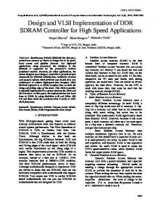
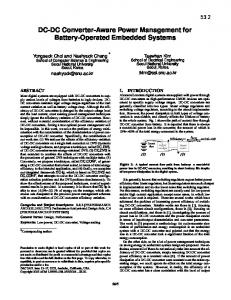
High Efficiency, 4.5V to 14V Input, Dual Output DDR Power Supply Figure 1 shows a DDR3 power supply that operates from a 4.5V to 14V input. Figure 2 shows efficiency curves for discontinuous and forced continuous modes of operation. Load-Release Transient Detection As output voltages drop, a major challenge for switching regulators is to limit the overshoot in VOUT during a load-release transient. The LTC3876 uses the DTR pin to monitor the first derivative of the ITH voltage to detect load release transients. Figure 3 shows how this pin is used for transient detection.
The LTC3876 features controlled on-time, valley current mode control, allowing it to accept a wide 4.5V to 38V input range, while supporting VDDQ outputs from 1.0V to 2.5V, and V TT and VTTR outputs from 0.5V to 1.25V. Its phase-locked loop (PLL) can be synchronized to an external clock between 200kHz and 2MHz. It also features voltage-tracking soft-start, PGOOD and fault protection. VIN 4.5V TO 14V
SENSE1+
15k
BOOST1
MT1
DB1
1μF
BOOST2
TG1
TG2
SW1
SW2
MT2
4.7μF
VOUTSENSE1+ VOUTSENSE1– PGOOD 0.1μF 15k
1000pF 100k
PGOOD TRACK/SS1
MB2 COUT4 330μF
BG2
SGND
70 65
VIN = 12V, DCM VIN = 12V, CCM VIN = 5V, DCM VIN = 5V, CCM 0
VTTR 2.2μF 1000pF
VTTR ±50mA
15k
ITH2 dn503 F01
Figure 1. 1.5V VDDQ/20A 0.75V VTT/10A DDR3 Power Supply 06/12/503
80 75
55
VTTSNS
RUN
COUT3 100μF
85
60
1μF
VTTRVCC
ITH1 RT
VTT 0.75V ±10A
DRVCC2
PGND
20k
100k
90
L2, 0.47μH
INTVCC BG1
95
3.57k
DB2 DRVCC1
MB1
15k
0.1μF
L1, 0.47μH
COUT2 330μF w2 30.1k
0.1μF
SENSE2+
0.1μF
EFFICIENCY (%)
0.1μF
3.57k
COUT1 100μF
L, LT, LTC, LTM, Linear Technology, the Linear logo and OPTI-LOOP are registered trademarks of Linear Technology Corporation. All other trademarks are the property of their respective owners.
VIN LTC3876 SENSE2– SENSE1–
CIN1 180μF w2
1.5V, 20A VDDQ
The two RITH resistors establish a voltage divider from INTVCC to SGND, and bias the DC voltage on the DTR pin (at steady-state load or ITH voltage) slightly above half of INTVCC. For a given CITH1, this divider does not
2
4
6 8 10 12 14 16 18 20 OUTPUT CURRENT (A)
dn503 F02
Figure 2. Efficiency of Circuit in Figure 1 (VDDQ = 1.5V, fSW = 400kHz, L = 470nH)
LOAD CURRENT 10A/DIV
INTVCC
1/2 INTVCC
ITH
+
LOAD RELEASE DETECTION TO LOGIC CONTROL
–
DTR
VOUT 100mV/DIV SW 5V/DIV
INTVCC CITH1
CITH2
VIN = 12V, VDDQ = 1.5V, IO = 0A TO 15A
dn503 F04a
VOVS = 127.5mV
RITH2
dn503 F03
a. LTC3876 DTR Disabled
RITH1
LOAD CURRENT 10A/DIV
Figure 3. Functional Diagram of DTR Connection for Load Transient Detection
change compensation performance as long as RITH1/ RITH2 equals RITH that would normally be used in conventional single-resistor OPTI-LOOP® compensation. The divider sets the RC time constant needed for the DTR duration. The DTR sensitivity can be adjusted by the DC bias voltage difference between DTR and half INTVCC. This difference could be set as low as 100mV, as long as the ITH ripple voltage with DC load current does not trigger the DTR. If the load transient is fast enough that the DTR voltage drops below half of INTVCC, a load release event is detected. The bottom gate (BG) is turned off, so that the inductor current flows through the body diode in the bottom MOSFET. Note that the DTR feature causes additional losses on the bottom MOSFET, due to its body diode conduction. The bottom FET temperature may be higher with a load of frequent and large load steps—an important design consideration. Test results show a 20°C increase when a continuous 100%-to-50% load step pulse chain with 50% duty cycle and 100kHz frequency is applied to the output. VTT Reference (VTTR) The linear V TT reference, VTTR, is specifically designed for large DDR memory systems by providing superior accuracy and load regulation for up to ±50mA output load. VTTR is the buffered output of the V TT differential reference resistor divider. VTTR is a high output linear reference, which tracks the V TT differential reference resistor divider and equals half of the remote-sense VDDQ voltage. Connect VTTR directly to the DDR memory VREF input. Both input and output supply decoupling are important to performance and accuracy. A 2.2μF output capaciData Sheet Download
www.linear.com
VIN = 12V, VDDQ = 1.5V, IO = 0A TO 15A
VOUT 100mV/DIV SW 5V/DIV
VOVS = 115mV
dn503 F04b
b. LTC3876 DTR Enabled
Figure 4. Load Release Comparison
tor is recommended for most typical applications. It is suggested to use no less than 1μF and no more than 47μF on the VTTR output. The VTTR power comes from the VTTRVCC pin. The typical recommended input VTTRVCC RC decoupling filter is 2.2μF and 1Ω. When VDDQSNS is tied to INTVCC, the VTTR linear reference output is 3-stated and VTTR becomes a reference input pin, with voltage from another LTC3876 in a multiphase application. VTT Supply The V TT supply reference is connected internally to the output of the VTTR V TT reference output. The V TT supply operates in forced continuous mode and tracks VDDQ in start-up and in normal operation regardless of the MODE/PLLIN settings. In start-up, the V TT supply is enabled coincident with the VDDQ supply. Operating the V TT supply in forced continuous mode allows accurate tracking in start-up and under all operating conditions. Conclusion The LTC3876 is a complete high efficiency and high accuracy solution for DDR memory power supplies. The unique controlled on-time architecture allows extremely low step-down ratios while maintaining a fast, constant switching frequency. The wide input voltage range of 4.5V–38V and programmable, synchronizable switching frequency from 200kHz to 2MHz gives designers the flexibility needed to optimize their systems. For applications help, call (408) 432-1900, Ext. 3598
Linear Technology Corporation
dn503f LT/AP 0612 196K • PRINTED IN THE USA
FAX: (408) 434-0507 ● www.linear.com
© LINEAR TECHNOLOGY CORPORATION 2012
1630 McCarthy Blvd., Milpitas, CA 95035-7417 (408) 432-1900
●