VLSI DESIGN 2001, Vol. 12, No. 3, pp. 349-363 Reprints available directly from the publisher Photocopying permitted by license only
(C) 2001 OPA (Overseas Publishers Association) N.V. Published by license under the Gordon and Breach Science Publishers imprint, member of the Taylor & Francis Group.
Exploiting Data-dependencies in Ultra Low-power DSP Arithmetic* V. A. BARTLETTa’t and E. GRASS b’ University
of Westminster, London, Englanc# blHP-GmbH, Frankfurt (Oder), Germany (Received 20 June 2000; In final form 3 August 2000)
Strategies for the design of ultra low power multipliers and multiplier-accumulators are reported. These are optimized for asynchronous applications being able to take advantage of data-dependent computation times. Nevertheless, the low power consumption can be obtained in both synchronous and asynchronous environments. Central to the energy efficiency is a dynamic-logic technique termed Conditional Evaluation which is able to exploit redundancies within the carry-save array and deliver energy consumption which is also heavily data-dependent. Energy efficient adaptations for handling two’s complement operands are introduced. Area overheads of the proposed designs are estimated and transistor level simulation results of signed and unsigned multipliers as well as a signed multiplier-accumulator are
given. Normalized comparisons with other designs show our approach to use less energy than other published multipliers. Keywords: Low-power; Array multiplier; DSP; Asynchronous systems; Data-dependent computation
1. INTRODUCTION
consumption. Such techniques span the design hierarchy from the algorithmic level down to process technology [1]. This paper addresses power minimization at the logic and circuit levels through reductions in circuit activity and switched capacitance. Asynchronous circuits have also been the subject of a growing body of research. Amongst
In many recently emerging portable applications of DSP circuits, maximizing battery life can be of paramount importance. In recent years, this has resulted in considerable research effort being directed at the development of VLSI design techniques for circuits with reduced power
* This work was supported by a grant from the U.K. Engineering and Physical Sciences Research Council, EPSRC. Address for correspondence: Dept. of Electronic Systems, University of Westminster, 115 New Cavendish Street, London W lW 6UW, UK. Tel.: +44 (0) 20 7911 5146, Fax: +44 (0) 20 7580 4319, e-mail:
[email protected] Tel.: +49 335 5625 731, Fax: +49 335 5625 671, e-mail:
[email protected]
349
350
V. A. BARTLETT AND E. GRASS
their attractions is the potential to achieve lowattributable largely to the power operation absence of a global clock and economies of circuitry which become possible. Another of their properties, which has attracted much attention, is the potential to exploit data-dependent delays. This gives rise, in principle, to a computational throughput which is average-case limited rather than worst-case limited. Although relatively few asynchronous VLSI designs have been reported, in many cases datadependent delays have been realized at the expense of low-power due to the adoption of differential logic styles such as DCVSL [2]. Whilst such styles readily facilitate Completion-Detection (CD), they are known to offer poor energy efficiency [1]. This paper reports strategies for the design of the building blocks of DSP computation namely which multipliers and multiplier-accumulators simultaneously achieve both ultra low-power operation and data-dependent delays. This is achieved by a synergy of architecture and circuitlevel implementation, neither of which alone, is responsible for the low energy consumption of the circuits. The architecture adopted for the basic multiplication operation is based on the carry-save array (CSA) proposed in [3] which exploits datadependent delays. This architecture has the property that much of its logic becomes redundant in proportion to the number of zeros in the multiplier
In this paper we extend that work by demonstrating that the synergy of architecture and implementation can be equally well applied to the design of signed multipliers and multiplieraccumulators to similar advantage. It should be noted that whilst the datadependency in terms of propagation delay is best exploited within an asynchronous framework, the high energy-efficiency can be obtained in both synchronous and asynchronous applications. Section 2 describes background material underpinning the main design considerations. Section 3 describes the data-dependent carry-save architecture and its application to multiplier and Concurrent Multiplier-Accumulator (CMAC) designs. Section 4 deals with adaptations to allow operation with 2’s complement operands. Implementation and timing issues are central to obtaining the maximum energy savings of the proposed approach these are discussed in Section 5. Simulation results and comparisons with other designs are presented in Section 6. Finally, conclusions are presented in Section 7.
2. BACKGROUND
In this paper, the goal of ultra low-power multiplication and multiply-accumulation has been achieved by the application of a number of different techniques, which are discussed below.
operand.
An issue not investigated in [3], however, is the potential for power reduction offered by this redundancy which can be exploited by inhibiting circuit activity within the redundant logic, as a function of input data. An implementation based on a hybrid static/dynamic logic CMOS circuit style lends itself readily to such exploitation. The feasibility of such an implementation was demonstrated by the authors in the design of an unsigned multiplier [4] using a technique we term ’Conditional Evaluation’ illustrating both low-power operation as well as other benefits in terms of low device-count and high-regularity.
2.1. Carry-save Array Multiplication Traditional carry-save array (CSA) multipliers comprise, in principle, an array of gated fulladders cells. In any single row of such cells, the ’gates’ perform the AND of the multiplicand with a single bit of the multiplier creating a ’bitproduct’. The sum of all bit-products emerges from the last row of the array as Sum and Carry vectors which must be added to produce the final result an operation involving full carry-propagation. This is carried out in a ’vector-merging’ or Carry-Resolution Adder (CRA).
DATA-DEPENDENT COMPUTATION
The terminology used in this paper is as follows. An n-bit multiplicand, MD, whose MSB is MDn-1 is multiplied by an m-bit multiplier, MR, whose MSB is MRm_ 1. The product of one bit of MR with MD produces a bit-product of nbits. The kth row of the array adds the incoming partial product to its bit-product thereby producing the kth partial product. The simple carry-save array is one of several approaches commonly used in multipliers to perform the summation of bit-products. Also widely used are tree structures, including those using 4:2 counters, and modified-Booth encoding which is applicable to both carry-save arrays and tree structures. Such strategies are known to offer improved worst-case latency over the simple carrysave array. However, as well as having less regularity, which complicates VLSI implementation, their architectures make the application of the energy saving conditional-evaluation technique more complex and less advantageous. Their use here, particularly in view of the attendant overheads, is not clearly justified since the primary design goal is low power. 2.2. Concurrent Multiply-Accumulation
In DSP algorithms, multiplication is very often followed by accumulation and time to perform a multiply-accumulate operation is often quoted as a performance measure of DSP hardware. Most commonly, multiply and addition operations are carried out separately in two cascaded hardware structures. Considerable benefits can, however, be obtained by carrying out the multiply and addition functions concurrently in the same structure, making use of the unused inputs around the periphery of a non-minimized CSA. An implementation of such a Concurrent Multiply-Accumulate (CMAC) structure was described in [5]. Since this approach exploits the otherwise unused inputs at the periphery of the CSA, the overall gate cost is considerably less than would be required to implement the addition separately. In comparison with conventional multiply-accumulate structures
351
a reduction in area of 20% has been reported [5]. Furthermore a reduction in latency of 50% (in a synchronous environment) was obtained.
2.3. Dynamic Logic
Use of dynamic logic for low-power operation inherently offers some advantages. In particular since each output can undergo, at most, one transition per evaluation, spurious transitions, which in static logic multipliers can account for as much as 50% of the energy consumption [6], are eliminated. Although spurious transitions can be addressed by other static-logic methods such as delay balancing [7], dynamic logic has the additional advantage of considerably reduced input capacitances due to the absence of a complementary logic tree. On the other hand, in comparison with static logic, dynamic CMOS circuits have two drawbacks which tend to offset the energy advantages. The first of these is the need to charge and discharge the precharge/evaluate lines. This normally takes place once per cycle although with the conditional-evaluation technique reported in this paper, on average it happens less frequently. The second is the increased probability of output activity which results from the fact that the precharge voltage precedes each valid output voltage. Whilst for some combinational functions this puts dynamic logic at a significant disadvantage [1], for others the increase in activity is small. In the implementations reported here the energy benefits considerably outweigh the drawbacks. Indeed, the fact that evaluation of dynamic logic can be inhibited by a single input recommends it naturally to activity reducing schemes. To avoid the race problem, dynamic-logic carrysave arrays usually employ differential circuitry [2, 3] despite its relatively poor energy efficiency [1]. Alternatively, the power benefits of single-ended logic can be obtained by using self-timing to avoid the race [8] and this was the approach adopted here. According to our own investigations, the technique has the additional advantage that
352
V. A. BARTLETT AND E. GRASS
charge-sharing problems, which with conventional dynamic logic can lead to increased transistor count, are eliminated. 2.4. Low-power Through Data-dependent Activity Reduction
Several techniques have been proposed for achieving low power by inhibiting circuit activity in combinational logic as a function of input data [6, 9, 10]. In general, these methods involve insertion of additional logic in the critical path, incurring some energy and delay penalty. The approach reported here differs from these methods. For example, the transformation of the standard carry-save-array architecture into that proposed in [3] entails the production of several additional outputs. Also, inhibition of activity in the redundant logic can be achieved with no delay penalty. 3. DATA-DEPENDENT ARCHITECTURES
3.1. Data-dependent Carry-save Array Multiplier Architecture
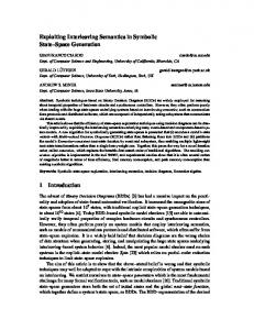
In the CSA multiplier architecture of [3] the array of AND gates normally used for bit-product generation is not needed. Instead, each cell in the array is fitted with a pair of multiplexers (MUXs) which, when a row’s bit-product is zero, pass on unaltered, the Partial-Product (PP) and Carry-In (CI) inputs from the row above, to the row below. For rows whose bit-product is non-zero, the MUXs select the adder outputs to feed to the row below. Since the propagation delay through the bypass path is less than that through the adders, values of MR which are heavily populated with zeros produce less delay through the array than those heavily populated with ones. An additional advantage of this architecture is its good testability due to the easy internal access provided by the MUXs. A comparison of the standard and data-dependent architectures is shown in Figure 1.
3.2. Concurrent Multiply-Accumulate Structure
As outlined above, the CMAC structure allows the CSA’s multiplication function to be augmented by accumulation and it offers a number of advantages over an implementation in which the two functions are carried out in separate hardware blocks. The reduction in gate count as well as the increase in regularity (which reduces interconnect capacitances) both have a beneficial impact on energy consumption. For synchronous applications, a pipelined implementation of the two separated functions can deliver some increase in throughput albeit at the cost of latency, energy and area. In asynchronous applications, however, pipelining has the effect of pushing average-case performance closer to the worst-case due to starvation and blocking effects [11]. The argument in favor of using the CMAC structure in low-power applications, is therefore valid for both synchronous and asynchronous circuits, but particularly so in the latter case. The general architecture of an 8+4 4-bit unsigned CMAC structure, based on the datadependent CSA, is shown in Figure 2. In order to accommodate growth in wordlength it is common to provide guard-bits in the accumulator. These can be included by extending the most significant end of the CRA. As with the multiplier discussed above, the aim here is to produce an asynchronous CMAC with reduced propagation delays and energy consumption by utilizing the data-dependency of the operation.
3.3. Carry-resolution Adder Conventional unsigned CSA multipliers require an n-bit adder for carry resolution. However, with the data-dependent CSA, the number of bits in the CRA is greater than n, requiring additional bits at the least significant end. This is because carries into the LSB of a row of the array can, if the row is in bypass mode, emerge from the array unresolved. In a stand-alone multiplier the first two rows of the CSA cannot produce (non-zero)
DATA-DEPENDENT COMPUTATION MD
PP
353
CI
MD
CI
MR(k) CRo|
%.
CRi
aR(k)
D
P
M
/
P coCI
PP
CRo
c,
PP
Carry-save array (CSA) architectures: standard (left) and data-dependent (right).
FIGURE
D7
CI
D6
D5
D4
D3
D2
DI
DO
MR0
MR1 MD3
MR2 MD3
MD2
MR3
e8
P7
P6
P5
P4
(n+m-3) bit adder
P3
P2
P1
P0
Shaded components for CMAC only
FIGURE 2 Unsigned Concurrent Multiply-Accumulate (CMAC) structure using data-dependent CSA.
unresolved carries and the number of bits required in the CRA is n-t-m-3 as shown in Figure 2. In the CMAC, (and in certain 2’s complement modifications to the multiplier described later) an additional CRA bit is required at the most significant end. Also, with the CMAC, since all rows except the first can produce unresolved
carries, one further adder-bit is needed at the least significant end. These additional bits are shown shaded in the CRA of Figure 2. The CRA used is a ripple-carry adder, chosen because of its minimal power dissipation. It is fitted with completion-detection circuitry and therefore the increase in average latency, due to
354
V. A. BARTLETT AND E. GRASS
the extra bits, is small. The Activity-Monitoring Completion-Detection (AMCD) method [12] is used. AMCD has certain advantages over other completion-detection methods. In particular, its silicon and energy overhead is small in comparison with other techniques especially when applied to domino CMOS [13]. A brief explanation of AMCD is given in Section 5. 4. HANDLING SIGNED OPERANDS
The structure of Figure 2 performs multiplication and multiply-accumulation on unsigned numbers. In many applications, however, the 2’s complement data representation is used. The following section presents a method of adapting the above architecture to handle such operands. 4.1. Two’s Complement Multiplier, MR
Array multipliers commonly use a simple modification to accommodate a 2’s complement representation of MR: since the MSB of a 2’s complement number carries a negative weight, instead of performing an addition of the bit-product to the partial-product in the mth (last) row of the array, a subtraction is carried out. The subtraction is often implemented by adding the l’s complement of MD together with a in its LSB position. The same algorithm can be implemented with the data-dependent CSA albeit with some alternative method of adding the extra 1. Since there are no unused inputs to the CRA at the appropriate position, the addition of the is carried out in the last row of the array by tying the unused input of the LSB’s carry-bypass MUX to a logic 1. The is therefore only selected when the row is performing an evaluation, as required.
product. In a row of the data-dependent array, the most significant carry-out represents the sign of the carry vector, only if the row evaluates in bypass mode the carry vector’s sign is represented by the row’s most significant carry-in. Therefore, sign extension can be implemented using an additional MUX to select the appropriate bit to extend. The sign-bit of the sum vector extends as normal. This method implies an increase in the fanout of the two extended signals, thereby adding delays to the critical path and increasing energy consumption. Furthermore, use of the PP input to the MSB cell for sign extension, precludes its use in the CMAC structure. For these reasons, this method was not used. An alternative which incurs no such penalties uses an arithmetic transform to convert each negative vector into a positive vector plus a (negative) correction term and has some similarities to the algorithm described in [14]. It is illustrated below by means of an example. For any single binary digit, d, the Boolean identity: d- 1- or more usefully -dcan be used to transform the negatively weighted MSB of each bit-product into its positivelyweighted complement minus 1. Hence the summation of bit-products in the carry save array can be transformed into the representation shown in Figure 3. Here, a row of 5 dots represents a 5 bit, bit-product and an overbar represents the complecorrection term). ment of a bit (shown with its By elimination of all negatively weighted bits
-
within the array, addition of the sum and carry vectors from each row can take place without signextension, the MSB of the partial product being simply the most-significant Carry-out of the row.
4.2. Two’s Complement Multiplicand, MD
In order to accommodate a 2’s complement representation of MD, several strategies can be adopted. The simplest involves sign extension of the MSBs of the two vectors representing a partial
FIGURE 3 Addition of transformed bit-products and correction term.
DATA-DEPENDENT COMPUTATION
The correction term is dealt with at the periphery of the array. This algorithm can be implemented in the datadependent CSA multiplier provided that care is taken with rows in bypass mode. Inversion of its sign-bit results in a bit-product which can take one of two possible values: MD4, MD3, MD2, MD1, MDo and 0 0 0 0 in evaluate and bypass mode respectively. Since the latter case corresponds to no computation in the row, the non-zero bit must be entered through one of the bypass MUXs. Two methods of achieving this were investigated. One uses a reconfiguration of the inputs to each row’s MSB cell as shown for the kth row in Figure 4(a) whilst the other requires some modification to the MSB cell itself, shown in Figure 4(b). Since both MD4 and MRk are available in both logic polarities anyway, neither method involves any increase in gate count. The circuit of Figure 4(a) has the advantage of using the unmodified cell at the cost of a slightly increased switched capacitance on MRs. The circuit of Figure 4(b), although modified, has no such associated energy cost and was chosen for that reason. Although the logic of both these circuits can be minimized, their structure is retained here for clarity. Whilst these solutions are adequate for a stand-alone multiplier, it should be noted that both preclude the combining of multiply and addition functions in the CMAC structure. The -1 -1 -1 -1 ’correction term’ can be dealt with most efficiently by Booth encoding it
355
into the equivalent form: -1 /0 /0 /0 /1 whose LSB, has a weight of 2"-1 (the same as the MSB of the multiplicand). Therefore this bit’s addition can most simply be performed in the most significant cell of the CSA’s first row, by tying its Carry-in to a logic 1. By doing so, however, a Carry-out can be produced which, in a stand-alone multiplier, would require extra circuitry down the left-hand side of the array. To avoid this, instead of applying the with weight 2 1, a string of s can be injected with weights 2 n-2 through 2 2 inclusive (thereby avoiding the most significant cell), together with a of weight 2 2 via the unused Carry-in input to the CRA. In other words the correction term is applied as:
-1 0 0 0 0 +1 +1 0 0
+1 The negatively weighted MSB of the correction term can be dealt with in the CRA by tying one of its MSB inputs to 1, ignoring any Carry thereby produced i.e., a modulo-two addition.
-
4.3. Two’s Complement Multiplicand in the CMAC
For reasons outlined above, simple sign-extension is undesirable. The arithmetic transform method can be applied to the CMAC structure with some modification to the implementation. The transformation of the bit-products into those with inverted
MR k
pp*
MD4
MD 4
CRo*
CRi
CRo*
MR k PPO
normally zero
(a)
PPO
CRi
MRk
CO
(b)
FIGURE 4 MSB cells for bit-product sign-bit inversion (a) unmodified (b) modified.
V. A. BARTLETT AND E. GRASS
356
MD 4
D
CI
CRo
CRi
o/
J MRk PPO
CO
FIGURE 5 MSB cell in row of CMAC for partial-product sign-bit inversion.
sign-bits cannot be carried out as in the case of the multiplier because the unused adder inputs are now required for summand, D. Therefore, bitproduct sign-bit inversion is carried out by replacing each row’s most significant cell with that shown in Figure 5. Here, the required to be injected at the MSB position when the row is in bypass-mode is combined with another input (here chosen to be the D input since the increase in capacitive load is placed off the critical path). By doing so, the injected becomes a two bit binary number of value (0 1) when D is zero and (1 0) when D is 1; in other words, of value: (D, D). Unlike the multiplier, the CMAC structure must anyway have circuitry (i.e., a MUX) to deal with the Carry-out from the most significant full-adder of each row. Consequently, addition of the positive bit of the correction term can be done more simply with the CMAC structure than with the multiplier, merely requiring that the top row’s most significant Cin input be tied to a logic 1. The negative bit of the correction term is dealt with, as before, in the MSB of the CRA.
5. IMPLEMENTATION AND TIMING 5.1. Interface to the Environment
The multiplier and CMAC circuits fit into the asynchronous framework for dynamic logic proposed in [15] i.e., the leading and trailing edges of
the START input, initiate the evaluation and precharge phases respectively. Similarly, the leading edge of the DONE signal indicates validity of the output data and its trailing edge indicates completion of the precharge phase. Such a protocol requires that the input operands are stable before the leading edge of the START signal and remain so throughout the computation. To ensure low-power operation, the circuits should not be left in the evaluation phase for longer than the dynamic storage time, otherwise charge leakage from dynamic storage nodes could cause short-circuit power dissipation in the domino inverters. This requirement is easily met in both synchronous and asynchronous applications, a handshake circuit suitable for the latter being described in [15].
5.2. Carry Save Array Using Conditional Evaluation
In the implementation of [4] significant energy savings derive from using a CSA comprising a combination of static logic for the MUXs and dynamic logic for the adders. The inclusion of static MUXs allows a row to function correctly in bypass mode with no transition on the precharge/ these remain in precharge mode evaluate lines until addition is called for. Assuming equal probabilities of ones and zeros in the bits of MR, on average only 50% of the precharge/evaluate lines will be driven for each multiplication, yielding a corresponding reduction in energy consumption. This, strategy, termed Conditional-Evaluation in [4], was shown to be an important mechanism for power reduction a row in bypass mode typically using less than one quarter of the energy of a row in which addition is performed. The structure of the CSA cell is shown in Figure 6(a). The inverters provide buffering to prevent excessive rise/fall times through the MUXs, (particularly important in bypass-mode). As outlined above, to maximize energy savings, single ended dynamic-logic was employed unlike the differential implementation of [3]. The
DATA-DEPENDENT COMPUTATION PP
MD
357
Cl
CarryEval
CRo