The digital signal is then passed to the channel simulator. The channel ..... for physical layer wireless network emulation," Vehicular Technology. Conference ...
FPGA-Based Channel Simulator for a Wireless Network Emulator Kevin C. Borries, Glenn Judd, Daniel D. Stancil, Peter Steenkiste Carnegie Mellon University Pittsburgh, PA Abstract— Wireless channel emulators are important tools for testing radio devices, especially in mobile environments. Wireless network emulators give the same accuracy and control for testing radio network systems that traditional channel emulators give to point to point radio links. Network emulators require many more independent channels than traditional channel emulators. This problem is particularly challenging for the real time channel simulator in the emulator. The challenges of designing a wireless network channel simulator are discussed and a design is presented on a Xilinx Virtex-II Pro FPGA. This channel simulator can model 210 independent channels between 15 nodes with a bandwidth of 90MHz. The performance of the design was verified by measuring transport-layer throughput between 802.11b radios transmitting through the channel simulator. Keywords- (channel simulator, emulator, wireless newtork, FPGA)
I.
INTRODUCTION
Wireless channel emulators have become a foundational tool for testing and verifying radio performance. The radio antenna ports are directly connected to the emulator testbed and the channel is simulated in real time with hardware. The emulator replicates the distortion from the wireless channel on the physical signals from the radios. The emulator channel properties can be updated through software so the simulated environments can be easily controlled. Emulators are much more realistic than computer simulations because real radio hardware is used to transmit and receive the radio frequency (RF) signals. Emulators also provide much more control and flexibility than real world wireless testbeds. The key to the channel emulator is the hardware channel simulator. The channel simulator must be fast to operate in real time, flexible to simulate many different environments and accurate to ensure that the radio signals are not distorted. There are a number of wireless emulators commercially available [1], [2] and developed in academia [3], [4] that provide both the bandwidth and channel flexibility for many applications. These emulators, however, do not provide the hundreds of independent channels required to support wireless networks with a reasonable number of nodes. A different emulator architecture is needed to provide a realistic, flexible and controllable testbed for wireless networks. This paper presents a channel simulator for a 15 node wireless emulator. Section II details the network emulator architecture. The tapped delay line (TDL) channel model and
Emulation Controller RF Front End Signal Conversion
RF Front End Signal Conversion RF Front End Signal Conversion
FPGA-based Channel Simulator
RF Front End Signal Conversion
Figure 1. Wireless network emulator system block diagram [5].
the design issues with implementing it on an FPGA are given in section III. The design is verified and performance results are given in section IV. II.
EMULATOR ARCHITECTURE
The general structure for a wireless network emulator was presented and verified with three nodes in [5]. A block diagram of the system is shown in Fig. 1. Laptops with wireless cards are placed in metal enclosures with an RF front end and signal conversion board. The RF signals from the laptops are downconverted by the RF front end and sampled by an analog to digital converter (ADC) on the signal conversion module. The digital signal is then passed to the channel simulator. The channel simulator attenuates, filters and combines all of the incoming signals to replicate a wireless environment. The configuration of the channel simulator is controlled by the emulator controller computer. The output of the channel simulator is converted to an analog signal by a digital to analog converter (DAC) on the signal conversion boards. The analog signal is then mixed up to RF by the RF front end. The current RF front end is designed for the 2.4GHz ISM band. The emulator can work in different bands but requires a new RF front end. The design of the RF front end for the emulator system was studied in [6]. The downconverted signal is sampled at 180MHz by an AD9430 12 bit ADC so the entire 80MHz of the 802.11b/g band can be emulated. A Virtex-4 FPGA on the signal conversion card synchronizes the sampled signal with the other cards and sends it to the channel simulator over a VHDCI
978-1-4244-2517-4/09/$20.00 ©2009 IEEE
Scale
…
Scale
Input 1
Output 1 Delay Pipe Scale
Input 2
Output 2
Delay Pipe
Scale Input 3
… Scale
… Scale
Delay Pipe
Scale Output 3
Figure 3. Tapped delay line channel model. The channel from input 3 to output 2 is multipath [5].
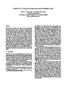
Figure 2. The FPGA channel simulator board.
cable. The Virtex-4 also receives signals from the channels simulator and synchronizes them with an AD9736 14 bit DAC. The channel simulator is a Virtex-II Pro FPGA on a very dense 18 layer board. A picture of the channel simulator board is shown in Fig. 2. The board has connections for 16 VHDCI ports of which 15 are connected to the signal conversion boards of each node. The remaining VHDCI port receives channel updates from the emulator controller.
have little impact on the performance of a wireless network. The phase shifts for non-resolvable multipaths, when τj is smaller than the symbol period, will produce fading which can be simulated by varying the magnitude of the paths. For time resolvable multipaths, τj is larger than the symbol period, the phase difference between paths will not dramatically impact the performance of a radio with good equalization.
The entire system is managed by the emulator controller computer. The controller first sets up an experiment with radio locations and environment settings, e.g. log scale path loss, multipath, fading K-factor. With the experiment data, the controller computes the channel losses and delays in real time and sends those channel settings to the channel simulator.
The structure of the tapped delay line for a three node network is shown in Fig. 3. The path delays τj are realized by the delay line and the scales represent the path scalar values, ai,j,k. The architecture in Fig. 3 is equivalent to the mathematical model, but the hardware realization of the TDL will deviate slightly from that model.
III.
NETWORK CHANNEL SIMULATOR DESIGN
A. Channel Model The channel for a wireless network in the ISM band can be accurately described by the tapped delay line (TDL) model [7]:
y k (t ) = ∑∑ ai , j ,k xi (t − τ j ) , i≠k
(1)
j
where yk is the signal received at destination node k and xi is the signal transmitted by node i. The received signal is the sum of scaled and shifted versions of the transmitted signals. The coefficient ai,j,k will be referred to as a path scalar because it defines a the gain of path j from the source i to the destination k. Similarly τj will be referred to as path delay. The sum of all the paths between two sources is defined as a channel. The signals in (1) are the actual RF signals, but in the emulator they must be mixed down to a lower frequency. Many channel simulators convert the signals to complex baseband to accurately simulate phase shifts in the channel. The channel phase is important in experiments with antenna arrays. However with single antenna radios, channel phase shifts will
B. Hardware Network Channel Simulator The embedded features of the Virtex-II Pro allow for a fast and expansive channel simulator. Two key components are the embedded block RAM, for the path delay, and the embedded multipliers, for the path scalar. One multiplier and block RAM pair create a single path in the TDL model. A single hardware path of the TDL model is shown in Fig. 4. The Virtex-II p50 has 232 multipliers each tied closely to a block of RAM. With a 15 node system and a single path per channel, 210 separate paths are required. Therefore, this FPGA can only create a few multipath channels while maintaining at least a single path between all the nodes. A more robust channel simulator can be created with very high end FPGAs, like the Virtex-5 SXT, that have over 1000 multipliers. 1) Scale Operation The path scale operation for the TDL is realized with an embedded multiplier followed by a bit shift operation. The two processes can be thought of as fine and coarse attenuation controls. The fine control of the multiplier allows for small resolution in the path attenuation, while the coarse control of the bit shifter produces a wide path dynamic range. Choosing the correct number of bits for each operation is crucial in the design of an accurate and efficient channel simulator.
From 12 Source ADC 8
7
Block RAM Delay
Embedded Multiplier
8
From Ethernet Controller
30
6
30
Bit Shift
Truncate
Scale Value
5
14 Shift Value
4
14 From Other Paths
Σ 14
Resolution (dB)
Delay Value
4 bit scale and 4 bit shift 8 bit scale and no shift R'
12
14 To Destination DAC
Figure 4. Path scale architecture
4
3
2
We assume for mathematical convenience that the incoming signal from the ADC will be multiplied by an integer value, n, between 1 and 2b, where b is the number of bits in the scalar multiplier. We also assume that the bit shift is to the right and is represented by the integer S which ranges from 0 to s. Therefore, for any general path the total path scalar is:
a = 2S n .
(2)
The subscripts in (2) have been removed for brevity. If there is no shift, the path step size, or resolution R (dB) at an integer value is defined as:
⎛ n + 1⎞ R = 20 log10 ⎜ ⎟. ⎝ n ⎠
(3)
Thus the path resolution decreases as n increases. The dynamic range D from n to 2b is:
D = 20b log10 (2 ) − 20 log10 (n ) .
0
0
10
20
30
40
50
Path Scale Value (dB)
Figure 5. Results of the latency test. The full latency system latency is 450ns
Fig. 5 shows that the resolution of the shifted values is at most the resolution at n = 2b-1. This resolution will be defined as:
⎛ 2 b−1 + 1 ⎞ R ′ = 20 log10 ⎜⎜ b−1 ⎟⎟ . ⎠ ⎝ 2
(6)
If Rmax≤R´ then the dynamic range with resolution finer than Rmax is the same with and without bit shifting, i.e. bit shifting does not extend the useful dynamic range. When Rmax>R´ the resolution of the shifted values satisfies the resolution requirement and the valid dynamic range is extended. The dynamic range for scalar values with bit shifting is:
(4)
For a given max channel resolution Rmax the smallest value of n that gives that has a resolution less than Rmax can be found from (3). By substituting this value of n into (4) the dynamic range can be found where the channel resolution is less than Rmax:
⎛ Rmax ⎞ D = 20b log10 (2 ) + 20 log10 ⎜⎜10 20 − 1⎟⎟ . ⎝ ⎠
1
(5)
From (5) the number of bits b required to represent a with a specified resolution and dynamic range can be found. For example, if Rmax = 0.1 dB and D = 30 dB then b = 11.4. Thus, 12 bits are needed to create a path with resolution less than 0.1 dB across a 30 dB dynamic range. Adding the shift operation dramatically increases the dynamic range but does not reduce the resolution. The bit shift operation expands the set of possible scale values. With a 2 bit shift the possible scalar values are not only 1 to 2b in integer steps (S = 0), but also included are the sets 2b + 2 to 2b+1 in steps of two (S = 1) and 2b+1+4 to 2b+2 in steps of four (S = 2).
⎡ ⎛ Rmax ⎞ ⎢20(b + s )log10 (2) + 20 log10 ⎜⎜10 20 − 1⎟⎟ Rmax > R′ . (7) ⎝ ⎠ D=⎢ max ⎢ ⎛ R20 ⎞ ⎢ 20b log10 (2) + 20 log10 ⎜10 − 1⎟ Rmax ≤ R′ ⎜ ⎟ ⎢⎣ ⎝ ⎠ Equation (7) shows that when Rmax>R´ the dynamic range for an 8 bit scalar value with no shift is equivalent to a 4 bit scalar value with a 4 bit maximum shift. This property is shown in Fig. 5. The following procedure can be used to find b and s. First compute b from (6) so that Rmax >R´. Then find s from (7) that satisfies the desired dynamic range. The scalar resolution has a direct impact on the accuracy and dynamic range of the channel simulator. The embedded multipliers can perform 18x18 multiplications at the system clock speed of 180MHz. To achieve a resolution of 0.1dB only 8 bits are needed. With an 8 bit scalar the embedded multiplier can run at twice the clock speed, 360MHz, allowing for two paths per physical multiplier.
TABLE I RESOURCES REQUIRED ON FPGA
Latency 0 ns
Resource
Used/Available
%Used
Slices LUTs Flip Flops BRAM Multipliers
16214/23616 22918/47232 15751/23616 24/232 226/232
68 52 33 10 97
Input Signal
Output Signal
The DAC has 14 bits of resolution so the output of the channel simulator must be truncated to 14 bits (Fig. 4). Truncation is done after the bit shift and before summing all of the paths together to reduce complexity in the path adder and minimize the overall system latency. On the other hand, truncation of the signal before the summation limits the dynamic range of the channel. With truncation there is a possibility of overflow after the scaling and shifting operations. Therefore, the path gain must be held below a maximum value. If the maximum path gain without overflow, amax, is less than 2b then the dynamic range is:
(8)
where the bit shifts are now to the left. With amax=4, a 14 bit shifter with Rmax = 0.1dB has a dynamic range of 57dB. The inputs and output to the adder are all 14 bits, so care must be taken to ensure that the adder does not overrun. The inputs to the path scalars are 12 bits so any path gain above 4 will cause an overrun. Also, if the sum of all the path gains is above 4, then there is a possibility of an overrun. The emulator controller can limit the simulation scenarios to not allow an overrun to occur. A path gain of 4 translates to a full system path loss of about 55dB, which is reasonably high for many practical indoor scenarios. The full path loss goes up to 55+57=117dB with a 0.1dB resolution, which will cause a loss of connection for most WLAN devices. 2) Delay Operation As mentioned before, the delays in the TDL are implemented by block RAM. The resolution of the delays is limited to the ADC sample rate of 180MHz, so the delay increment is ~5.56ns. The delay step size is much less than the sample time of most common radio devices that operate in the 2.4GHz ISM band. Therefore, time resolvable multipath can be simulated down to one sample period. The maximum delay depends on the amount of memory available per path. With 18 kbits per path of block RAM and 12 bits per sample, each path can delay the input signal up to ~8.53μs, which is a sufficiently large path loss even for outdoor environments.
125 ns
Central FPGA
SCM1 FPGA
ADC
250 ns
450 ns
The current design implements a 14 bit maximum shift which gives a dynamic range of about 94dB with Rmax = 0.1dB. However, the full dynamic range is not used because of the limitations on the path summation and the bit resolution of the DAC.
⎛ ⎛ Rmax ⎞⎞ D = 20 log10 ⎜ 2 s a max ⎜⎜10 20 − 1⎟⎟ ⎟ , ⎟ ⎜ ⎝ ⎠⎠ ⎝
78 ns
215 ns
SCM2 FPGA
DAC
Channel Simulator
Virtex II – Pro
Figure 6. Results of the latency test. The full latency system latency is 450ns
Like the embedded multipliers with 8 bit scalar resolution, the block RAM can run at 360MHz. By multiplexing the multipliers and the RAM the number of paths in each channel can be doubled. However, this feature is not implemented on the current design. 3) Channel Updates One of the key features of the emulator system is the ability to simulate mobility. In mobile experiments the path scaling values and delays must be updated regularly due to fading. As described in section II the path scale and delay values are generated on the emulator controller PC and sent to the channel simulator. The data is sent over a 100Mbps Ethernet line to an auxiliary FPGA that converts the Ethernet packet to messages for the channel simulator. In the current design all of the path and delay values can be updated at a rate of about 1ms. With this update rate, accurate fading can be generated for mobiles with speeds up to 60m/s (216km/hr). 4) Current Design The current design uses 226 paths: 202 channels with a single path and 8 channels with 3 paths. For channels with a single path, the block RAM delay is not implemented to save space in routing. The full realization of the channel simulator is able to fit on the Virtex-II p50. The resource usage is given in Table I. IV.
VERIFICATION
The performance of the emulator was tested by measuring the system latency, observing the spectrum of the output RF signal and comparing emulator generated throughput tests with throughput tests in a physical environment. Each of these tests showed that the emulator produced an accurate simulation of the wireless channel. The time a signal takes to go through the emulator, the system latency, is much slower than the propagation time of a typical wireless signal. The 802.11b/g standard limits the maximum propagation time to 1μs. Thus as long as the system latency is below 1μs, 802.11b/g radios will function normally. The latency of the emulator was measured directly by inputting a pulsed RF signal, probing the power at different points on the boards and measuring the time difference in the pulses with a 100MHz oscilloscope. The full system latency is shown in Fig. 6. The latency from the RF front end is not included because it is very short and close to the measurement
error. A large percentage of the system latency is due to the DAC. The AD9736 DAC was chosen for this design because of the wide bandwidth and low output noise. The DAC also has some sophisticated clock recovery and data synchronization features. However, these features add significant latency to the DAC. Even with the additional delays from the DAC the full system latency is still well below the 1μs threshold. The multipath channel was verified by measuring the spectrum of the RF output with and without multipath. The results are shown in Fig. 7. The multipath channel has 3 taps with fixed power and relative delays: tap1: 60dB, 0ns, tap2: 66dB, 278ns, tap3: 63dB, 456ns. The input signal was an 802.11b packet. Without multipath in the channel the spectrum is a clean 802.11b envelope. With multipath the spectrum is distorted by the transfer function of the channel. Fig. 7 shows a close agreement with the theoretical output spectrum with the spectrum that was observed. The main goal of the emulator is to reproduce a wireless channel in a controlled environment, i.e. radios connected to the emulator testbed should perform the same as if they were in a real wireless environment. The realism of the emulator was tested by measuring the throughput between two 802.11b radios connected to the emulator and comparing the results with the same test in a controlled physical environment. The 802.11b radios ran a TCP throughput test with the iperf command. The throughput tests were also performed with the radios connected through a coax cable with a step attenuator. The results of the tests are shown in Fig. 8. The 2dB difference in signal strength is within the error of the step attenuator. The results show that the emulator produces a physical channel similar to the natural wireless environment with minimum unwanted distortion to the physical signal.
-55
V.
CONCLUSION
A wireless network channel emulator demands many more channels from the channel simulator hardware than a point-topoint emulator. An FPGA design for the channel simulator was presented to satisfy the demands of a network emulator. The design utilized embedded multipliers and embedded block RAM on the FGPA. The accuracy of the channel simulator was analyzed mathematically and also verified through hardware measurements. The full emulator system accurately reproduced transport–layer experiments run in a physical environment. REFERENCES [1] [2] [3]
[4] [5] [6]
[7]
http://www.elektrobit.com/file.php?113 http://www.smartsim.at/folder/A0100437.3.web_v310804.pdf Sylvie Picol; Gheorghe Zaharia; Dominique Houzet; Ghais el Zein, "Hardware simulator for MIMO radio channels: design and features of the digital block," Vehicular Technology Conference, 2008. VTC2008Fall. IEEE 68th , Sept. 2008 M. Kahrs and C. Zimmer, “Digital signal processing in a real-time propagation simulator,” IEEE Trans. Instrum. Meas., vol. 55, no. 1, pp. 197-205, Feb. 2006. G. Judd and P. Steenkiste. Using Emulation to understand and improve wireless networks and applications. Proceedings of NSDI 2005, May 2005. Judd, G.; Steenkiste, P., "Design and implementation of an RF front end for physical layer wireless network emulation," Vehicular Technology Conference, 2007. VTC2007-Spring. IEEE 65th , vol., no., pp.974-979, 22-25 April 2007 Turin, G.L.; Clapp, F.D.; Johnston, T.L.; Fine, S.B.; Lavry, D., "A statistical model of urban multipath propagation," Vehicular Technology, IEEE Transactions on , vol.21, no.1, pp. 1-9, Feb 1972
Multipath On Multipath Off Theoretical Multipath
Controlled Attenuation Through Emulator
6
-60
Througput (Mbps)
Amplitude (dBm)
5 -65
-70
-75
3
2
-80
-85 2.4
4
1
0 2.405
2.41
2.415 2.42 Frequency (Hz)
2.425
2.43 9
x 10
Figure 7. Spectrum of a 802.11b signal on channel 2 after going through the emulator with and without multipath enabled. The theoretical multipath is the original envelope multiplied with the transfer function of
85
90
95
100 105 110 115 Channel Loss (dB)
120
125
130
Figure 8. Throughput of data over a controlled attenuation cable compared with that of the emulator system. Test was run on channel 6 with 802.11b radios.