hardware platforms that provide the technology for realizing the rapidly expanding digital wireless communication infrastructure. Many sophisticated signal ...
(IJACSA) International Journal of Advanced Computer Science and Applications, Vol. 2, No. 5, 2011
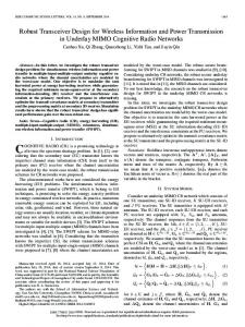
FPGA-Based Design of High-Speed CIC Decimator for Wireless Applications Rajesh Mehra
Rashmi Arora
ECE Department, National Institute of Technical Teachers„ Training & Research Chandigarh, India
M.E. Student, ECE Department, National Institute of Technical Teachers„ Training & Research Chandigarh, India
Abstract— In this paper an efficient multiplier-less technique is presented to design and implement a high speed CIC decimator for wireless applications like SDR and GSM. The Cascaded Integrator Comb is a commonly used decimation filter which performs sample rate conversion (SRC) using only additions/subtractions. The implementation is based on efficient utilization of embedded LUTs of the target device to enhance the speed of proposed design. It is an efficient method used to design and implement CIC decimator because the use of embedded LUTs not only increases the speed but also saves the resources on the target device. The fully pipelined CIC decimator is designed with Matlab, simulated with Xilinx AccelDSP, synthesized with Xilinx Synthesis Tool (XST), and implemented on Virtex-II based XC2VP50-6 target FPGA device. The proposed design can operate at an estimated frequency of 276.6 MHz by consuming considerably less resources on target device to provide cost effective solution for SDR based wireless applications.
performed in SDR, including advanced compression algorithms, power control, channel estimation, equalization, forward error control, adaptive antennas, rake processing in a WCDMA (wideband code division multiple access) system and protocol management.
Keywords- CIC; FPGA; FPGA; GSM; LUT; SDR.
On one hand, high development costs and time-to-market factors associated with ASICs can be prohibitive for certain applications while, on the other hand, programmable DSP processors can be unable to meet desired performance due to their sequential-execution architecture [6]. In this context, embedded FPGAs offer a very attractive solution that balance high flexibility, time-to-market, cost and performance.
I. INTRODUCTION The widespread use of digital representation of signals for transmission and storage has created challenges in the area of digital signal processing [1]. The applications of digital FIR filter and up/down sampling techniques are found everywhere in modem electronic products. For every electronic product, lower circuit complexity is always an important design target since it reduces the cost [2]. There are many applications where the sampling rate must be changed. Interpolators and decimators are utilized to increase or decrease the sampling rate. This rate conversion requirement leads to production of undesired signals associated with aliasing and imaging errors. So some kind of filter should be placed to attenuate these errors [3]. Recently, there is increasingly strong interest on implementing multi-mode terminals, which are able to process different types of signals, e.g. WCDMA, GPRS, WLAN and Bluetooth. These versatile mobile terminals favor simple receiver architectures because otherwise they‟d be too costly and bulky for practical applications [4]. The answer to the diverse range of requirements is the software defined radio. Software defined radios (SDR) are highly configurable hardware platforms that provide the technology for realizing the rapidly expanding digital wireless communication infrastructure. Many sophisticated signal processing tasks are
Today‟s consumer electronics such as cellular phones and other multi-media and wireless devices often require digital signal processing (DSP) algorithms for several crucial operations[5] in order to increase speed, reduce area and power consumption. Due to a growing demand for such complex DSP applications, high performance, low-cost Soc implementations of DSP algorithms are receiving increased attention among researchers and design engineers. Although ASICs and DSP chips have been the traditional solution for high performance applications, now the technology and the market demands are looking for changes.
The digital signal processing application by using variable sampling rates can improve the flexibility of a software defined radio. It reduces the need for expensive anti-aliasing analog filters and enables processing of different types of signals with different sampling rates. It allows partitioning of the highspeed processing into parallel multiple lower speed processing tasks which can lead to a significant saving in computational power and cost. Wideband receivers take advantage of multirate signal processing for efficient channelization and offers flexibility for symbol synchronization. II. CIC DECIMATORS First, confirm that you have the correct template for your paper size. This template has been tailored for output on the US-letter paper size. If you are using A4-sized paper, please close this file and download the file for “MSW A4 format”. The Cascaded Integrator Comb (CIC), first introduced by Hogenauer, presents a simple but effective platform for implementation of decimations. It is a commonly used 59 | P a g e
www.ijacsa.thesai.org
(IJACSA) International Journal of Advanced Computer Science and Applications, Vol. 2, No. 5, 2011
decimation filter which performs sample rate conversion (SRC) using only additions/subtractions. It then has experienced some modifications toward improvements in power consumption and frequency response [7]-[8]. It consists of two main sections: an integrator and a comb, separated by a down-sampler [9]-[10]. An integrator is simply a single-pole IIR filter with a unity feedback coefficient:
y[n] y[n 1] x[n]
When we build a CIC filter, we cascade, or chain output to input, N integrator sections together with N comb sections. This filter would be fine, but we can simplify it by combining it with the rate changer. Using a technique for multi-rate analysis of LTI systems from [13], we can “push" the comb sections through the rate changer, and have them become at the slower sampling rate fs/R.
y[n] x[n] x[n M ]
(1)
The transfer function for a CIC filter at fs is
This system is also known as an accumulator. The transfer function for an integrator on the z-plane is
H I ( z)
1 1 z 1
H ( z ) H IN ( z ) H CN ( z ) RM 1 (1 z RM ) N H ( z) ( z k ) N 1 N (1 z ) k 0
(2)
The power response of integrator is basically a low-pass filter with a -20 dB per decade (-6 dB per octave) rolloff, but with infinite gain at DC [11]. This is due to the single pole at z = 1; the output can grow without bound for a bounded input. In other words, a single integrator by itself is unstable and shown in Figure 1
(5)
(6)
This equation shows that even though a CIC has integrators in it, which by themselves have an infinite impulse response, a CIC filter is equivalent to N FIR filters, each having a rectangular impulse response. The CIC filter has a high passband droop and a low stop-band attenuation, which can be improved by increasing the number of the cascaded CIC filters [14]. Sharpening based methods generally improve both the pass-band and the stop-band characteristic of the CIC filter at an expense of the increased complexity [15]. Since all of the coefficients of these FIR filters are unity, and therefore symmetric, a CIC filter also has a linear phase response and constant group delay [16]. The magnitude response at the output of the filter can be shown to be: N
Figure 1. Basic Integrator
H( f )
A comb filter running at the high sampling rate, fs, for a rate change of R is an odd symmetric FIR filter described by
y[n] x[n] x[n RM ]
(3)
Where M is a design parameter and is called the differential delay. M can be any positive integer, but it is usually limited to 1 or 2. The corresponding transfer at fs
H c ( z) 1 z RM
(4)
When R = 1 and M = 1, the power response is a high-pass function with 20 dB per decade (6 dB per octave) gain (after all, it is the inverse of an integrator). When RM ≠ 1; the power response takes on the familiar raised cosine form, with RM cycles from 0 to 2π. The basic comb is shown in Figure 2.
SinMF f Sin R
(7)
By using the relation sin x x for small x and some algebra, we can approximate this function for large R as
SinMF 1 (8) for 0 f MF M We can notice a few things about the response. One is that the output spectrum has nulls at multiples of f = 1/M. In addition, the region around the null is where aliasing/imaging occurs. If we define fc to be the cutoff of the usable passband, then the aliasing/imaging regions are at N
H ( f ) RM
for
(i f c ) f (i f c ) 1 M f and i = 1, 2,……[R/2]. If f c 2 2
(9) ,
then the maximum of these will occur at the lower edge of the first band, 1-fc. The system designer must take this into consideration, and adjust R, M, and N as needed. Another thing we can notice is that the passband attenuation is a function of the number of stages. As a result, while increasing the number Figure 2. Basic Comb
60 | P a g e www.ijacsa.thesai.org
(IJACSA) International Journal of Advanced Computer Science and Applications, Vol. 2, No. 5, 2011
of stages improves the imaging/alias rejection, it also increases the passband “droop."
as shown in Figure 5 The complete Matlab to AccelDSP design flow is shown in Fig6.
III. PROPOSED CIC DECIMATOR DESIGN & SIMULATION In this proposed work fully pipelined 3-stage CIC decimator is designed using Matlab and Xilinx AccelDSP by taking filter R as 8 and M as 2. Figure 5. CIC Decimator
Figure 6. AccelDSP Design Flow
Figure 3. Floating Point Output of CIC Decimator
The Matlab based floating point output of proposed design is shown in Fig 3. Then the equivalent fixed point file is generated and verified by AccelDSP whose output is shown in Fig4. The red wave shows the input sequence, green wave shows the ideal response and blue plot is the output from CIC decimator.
The proposed design shows an efficient realization of CIC decimator by using embedded LUTs of target FPGA to provide high speed operation. The multiplier less LUT based technique consist of input registers, 4-input LUT unit and shifter/accumulator unit as shown in Fig7.
Figure 7. LUT based Multiplier Less Implementation
IV. FPGA IMPLEMENTATION RESULTS To observe the speed and resource utilization, RTL is generated, verified and synthesized. The proposed CIC decimator filter is implemented on Virtex-II Pro based XC2VP50-6 target device using fully pipelined LUT based multiplier less technique. The resource utilization of proposed implementation is shown in table I.
Figure 4. Fixed Point Output of CIC Decimator
The 3 stage CIC decimator is designed to accomplish three things here. First, we have slowed down half of the filter and therefore increased efficiency. Second, we have reduced the number of delay elements needed in the comb sections. Third, and most important, the integrator and comb structure are now independent of the rate change. This means we can design a CIC filter with a programmable rate change and keep the same filtering structure. A CIC decimator would have N cascaded integrator stages clocked at fs, followed by a rate change by a factor R, followed by N cascaded comb stages running at fs/R
TABLE I.
VIRTEX-II PRO BASED RESOURCE UTILIZATION
61 | P a g e www.ijacsa.thesai.org
(IJACSA) International Journal of Advanced Computer Science and Applications, Vol. 2, No. 5, 2011 TABLE II.
TRANSPOSED FORM PERFORMANCE EVALUATION
[7]
[8]
[9] TABLE III.
LOGIC UTILIZATION COMPARISON ON VIRTEX-II PRO BASED XC2VP50-6 FPGA
[10]
[11] [12]
[13]
[14]
As shown in table III, the proposed LUT based design can work at an estimated frequency of 276.6 MHz as compared to 156 MHz in case of [3] by using considerable less resources of target FPGA. The speed performance of proposed design is shown in table II. V.
[15]
[16]
CONCLUSION
In this paper, a Xilinx AccelDSP based approach is presented for a CIC Decimator to minimize the time to market factor. The proposed fully pipelined CIC decimator filter is designed by using embedded LUTs of target device. The results show enhanced performance in terms of speed and area utilization. The proposed transposed design can operate at an estimated frequency of 276.6 MHz by consuming considerably less resources available on target device to provide cost effective solution for SDR based wireless communication applications.
[17]
[18]
[19]
[20]
REFERENCES [1]
[2]
[3]
[4]
[5]
[6]
Vijay Sundararajan, Keshab K. Parhi, “Synthesis of Minimum-Area Folded Architectures for Rectangular Multidimensional”,IEEE Transactions on Signal Processing, pp. 1954-1965, Vol. 51, No.7, July 2003. ShyhJye Jou, Kai-Yuan Jheng*, Hsiao-Yun Chen and An-Yeu Wu, “Multiplierless Multirate Decimator I Interpolator Module Generator”, IEEE Asia-Pacific Conference on Advanced System Integrated Circuits, pp. 58-61, Aug-2004. Amir Beygi, Ali Mohammadi, Adib Abrishamifar. “AN FPGA-BASED IRRATIONAL DECIMATOR FOR DIGITAL RECEIVERS”, in 9th IEEE International Symposium on Signal Processing and its Applications, pp. 1-4, ISSPA-2007. K. B. Huang, Y. H. Chew, and P. S. Chin “A Novel DS-CDMA Rake Receiver: Architecture and Performance”,IEEE International Conference on Communications, pp-2904-2908, ICC-2004. D.J. Allred, H. Yoo, V. Krishnan, W. Huang, and D. Anderson, “A Novel High Performance Distributed Arithmetic Adaptive Filter Implementation on an FPGA”, in Proc. IEEE Int. Conference on Acoustics, Speech, and Signal Processing (ICASSP‟04), Vol. 5, pp. 161164, 2004. Patrick Longa and Ali Miri “Area-Efficient FIR Filter Design on FPGAs using Distributed Arithmetic”, IEEE International Symposium on Signal Processing and Information Technology, Vol. 4, pp.248-252, 2006.
[21]
F.J.A. de Aquino, C.A.F. da Rocha, and L.S. Resende, “Design of CIC filters for software radio system”, IEEE International Conference on Acoustics, Speech, Signal Processing, May 2006. E. B. Hogenauer, “An economical class of digital filters for decimation and interpolation”, IEEE Transactions on Acoustics,Speech, Signal Processing, Vol. ASSP-29, pp. 155-162, April 1981. R. Uusikartano, and J. Takala, “Power-efficient CIC decimator architecture for fs/4-downconverting digital receivers”, IEEE International Midwest Symposium on Circuits and Systems, Dec. 2004. G. Jovanovic Dolecek, S.K. Mitra, “ Efficient Comb-Rotated Sinc (RS) Decimator With Sharpened Magnitude Response”, IEEE International Midwest Symposium on Circuits and Systems,2004. Matthew P. Donadio, “CIC Filter Introduction”, IEEE International Symposium on Communications , July 2000. W.A. Abu-Al-Saud, and G.L. Stuber, “Modified CIC filter for sample rate conversion in software radio systems”, IEEE Signal Processing Letters, Vol. 10, Issue: 5, pp. 152-154, May 2003. G.J. Dolecek, and J.D. Carmona, “A new cascaded modified CIC-cosine decimation filter”, IEEE International Symposium on Circuits and Systems, May 2005. M. Becker; N. Lotze et al; “Implementation of a Power Optimized Decimator for Cascaded Sigma-Delta A/D Converters”, in ICSES, pp. 83-86, 2004. Quan Liu; Jun Gao; “On Design of Efficient Comb Decimator with Improved Response for Sigma-Delta Analog-to-Digital Converters”, International Conference on image and signal processing, pp. 1-5, 2009. G. Jovanovic Dolecek; S.K. Mitra; “Two-stage CIC-based decimator with improved characteristics”, in IET Signal Process., Vol. 4, pp. 22– 29, Oct 2010. Alfonso Fernandez-Vazquez, Gordana Jovanovic Dolecek, “Passband and Stopband CIC Improvement Based on Efficient IIR Filter Structure”, IEEE Transactions on Circuits and Systems, Vol. 52, No. 7, July 2005. H. Aboushady; Y. Dumonteix; M. Louerat; and H. Mehrez; “Efficient polyphase decomposition comb decimation filters in sigma–delta analog–digital converter”, IEEE Trans. Circuits Syst. II, Analog Digit.Signal Process., Vol. 48, No. 10, pp. 898–903, Oct. 2001. Gordana Jovanovic-Dolecek, Sanjit K. Mitra, “A New Two-Stage Sharpened Comb Decimator”, IEEE Transactions on Circuits and Systems, Vol. 52, No. 7, July 2005. Y. Gao; L. Jia, J. Isoaha; and H. Tenhunen; “A comparison design of comb decimators for sigma–delta analog-to-digital converters”, Analog Integr. Circuits Signal Process., Vol. 22, No. 1, pp. 51–60, Jan. 2000. Chakraborty, R. (2011). FPGA Based Cipher Design & Implementation of Recursive Oriented Block Arithmetic and Substitution Technique ( ROBAST ). International Journal of Advanced Computer Science and Applications - IJACSA, 2(4), 54-59. AUTHORS PROFILE Mr. Rajesh Mehra is currently Assistant Professor at National Institute of Technical Teachers‟ Training & Research, Chandigarh, India. He is pursuing his PhD from Panjab University, Chandigarh, India. He has completed his M.E. from NITTTR, Chandigarh, India and B.Tech. from NIT, Jalandhar, India. Mr. Mehra has 15 years of academic experience. He has authored more than 15 research papers in reputed International Journals and 35 research papers in National and International conferences. Mr. Mehra‟s interest areas include VLSI Design, Embedded System Design, Advanced Digital Signal Processing, Wireless & Mobile Communication and Digital System Design. Ms Rashmi Arora received her B.E. Degree with Honors in Electronics & Communication engineering from M.J.P. Rohilkhand University, Bareilly, U.P., India, in 2002. She is currently pursuing her M.E. degree from NITTTR, Chandigarh, India. She has 7 years of academic experience. Her interest areas are Signal Processing, Embedded Systems and VLSI Design.
62 | P a g e www.ijacsa.thesai.org