Open Eng. 2016; 6:174–184
Research Article
Open Access
Kennedy Adinbo Aganah* and Olorunfemi Ojo
Generalized Carrier-Based PWM Method for a 12-Switch Converter DOI 10.1515/eng-2016-0022 Received May 29, 2015; accepted Jun 23, 2016
Abstract: This paper proposes a generalized carrier-based pulse-width modulation (CBPWM) method for a 12-switch converter feeding three independent loads. The converter topology is part of the (3N + 3)-switch converter family where N is the number of outputs (N = 3 for this special case). Its more famous sibling is the 9-switch converter which is gaining considerable interest from researchers because of its reduced-switch count architecture. The structure and limitations of the converter are elaborated; its modulation method applicable to both equal and different frequency (and/or amplitude) operations is formulated. The generalized neutral voltages for the converter is derived for the first time and used as the offset voltages required by this type of topology to decouple its three outputs. The proposed algorithm is validated by both theoretical simulations and experimental results. Keywords: reduced-switch-count; nine-switch inverter; carrier-based pwm; ac drive; twelve-switch inverter
1 Introduction In most modern industrial processes, high-performance control of AC machines is achieved using voltage source converters (VSCs). A typical process may require independent control of several AC machines. Usually, this function is implemented using a separate converter per machine. However, in medium to high power applications, the cost of power electronics becomes an important design constraint. An increasingly accepted alternative to full-switch count VSCs is to use reduced-switch count VSC topolo-
*Corresponding Author: Kennedy Adinbo Aganah: Department of Electrical Engineering, College of Engineering, Tuskegee University, Tuskegee, AL 36088, U.S.A.; Email:
[email protected] Olorunfemi Ojo: Department of Electrical and Computer Engineering/CESR, Tennessee Technological University, Cookeville, TN 38505, U.S.A.; Email:
[email protected]
gies [1–14]. The 5−leg inverter [1, 2]; 4-leg inverter [3, 4]; 6and 3-switch converters [5]; 4-switch inverter [6]; 9-switch inverter [10–14]; and multilevel converters [8, 9] are but a few examples. Most of the reduced-switch count topologies can be categorized into three main types; in the first category, reduction in switch count is achieved by replacing a switched-leg with a split-capacitor-leg and sharing this split-capacitor-leg between two outputs (or phases) [5, 6]. The drawback of this topology is the appearance of unbalance capacitor voltages and the associated uneven stress on the devices. An improved topology replaces the capacitor-leg with a switched-leg. These are the so-called (2n + 1)−leg converters [7] and the 5−leg converter is special case of this type [1, 2]. A third type of reduced-switch count VSCs which has gained prominence lately, is implemented by sharing a row of switches between neighboring outputs (or phases). The 9-switch converter [10–14] is an example of this type. In fact, the 9-switch converter can be considered as a special case of the generalized (3N + 3)switch converter introduced in [10] for N = 2 (N represents the number of independent three-phase outputs). The 6-switch converter [5] is a hybrid of the split-capacitorleg[5, 6] and the (3N + 3)-switch topologies [10–15]. The net gain from using reduced number of switching devices in VSCs may at first seem insignificant. For example, in the 5−leg topology [1, 2] there is a reduction of only two switching devices compared to the full-switch topology. However, the reduced-switch count is accompanied by elimination of accompanying complex gate driver and protection circuits. Thus, the overall system can be significantly less expensive, smaller size and lighter in weight. These gains, however, come with structural limitations. The sharing of legs or switches between outputs (or phases) inherently couples the sharing partners and imposes switching constraints on the converter that must be catered for by an appropriate switching algorithm. Since the 9-switch was first introduced [10–12], several researches have attempted to remedy its shortcomings and thereby increase its appeal. These efforts have resulted in applications such as uninterruptible power supplies (UPS) [12, 16], adjustable speed motor drive [13], sixphase motor drive [17], unified power quality conditioner
© 2016 K. A. Aganah and O. Ojo, published by De Gruyter Open. This work is licensed under the Creative Commons Attribution-NonCommercial-NoDerivs 3.0 License.
Unauthenticated Download Date | 7/8/16 4:05 PM
GCB-PWM Method for a 12-Switch Converter | 175
Qa 1 Vdc/2
Q b1 a1
Q a2
b1 Q b2
a2
c1 Qc2
b2 Q b3
a3
Vdc/2
Qa 4
Qc3
b3 Q b4
z1 M1
c2
o Q a3
2 Structure and Switching Limitations
Qc1
z2 M2
c3 Q c4
z3 M3
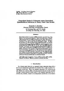
Figure 1: Structure of the 12-switch converter.
(UPQC) [18, 19], renewable energy integration system [20– 23], and hybrid/electic vehicles[24]. Kominami et al. [10] extended the concept of the 9switch converter to a generalized (3N +3)-switch converter for independently supplying N three-phase loads. However its limitations and modulation scheme has not been adequately addressed. As reported in [10–14, 25], the two outputs of the 9-switch converter are decoupled by injecting some DC voltage to the two modulating signals so that its the switching constraint is not violated. So far, however, there has been little discussion about how these ‘appropriate’ offsets are chosen. For example, whereas Kominami et al. inject one-fourth of the input DC voltage to upper reference and subtracts same from the lower reference, Gao et al. [25] inject the maximum and minimum of the phase voltages to the upper and lower references respectively. In this paper, a generalized Carrier-Based PulsedWidth Modulation (CBPWM) method for the 12-switch converter is proposed. It utilizes its neutral voltages similar to that derived in [15]. It can be shown that when the derived neutral voltages are injected into the reference voltage commands; its three outputs are decoupled and can be treated as three ‘independent’ VSCs. The validity of the proposed modulation strategy is verified by both simulations and experimental results. This paper is organized as follows: following the introduction, the structure of the converter is presented in Section 2. The proposed modulation strategy is developed and implemented in Section 3. Simulation and experimental results from a laboratory prototype are presented in Section 4 and finally, conclusions are drawn in Section 5.
Fig. 1 shows the structure of the (3N + 3)-switch converter supplying N independent three-phase induction machines (IMs). The switching devices are represented by Q ij where the subscript i ∈ [a, b, c] refer to the three phases and the second index, j ∈ [1, 2, . . . , N + 1], show the position of a switch in a phase-leg. The machines (or outputs) are represented by IMk , (or Invk) where k ∈ [1, 2, . . . , N] refer to the position of the machine (or output) in the N-machine (or N−output) system. In this paper, it is assumed that the neutral points, zk, of the machines are isolated from one another. A distinct feature of this topology is the sharing of row of switches between neighboring outputs. Except for the topmost and bottommost switch rows (i.e. k = 1 and k = N), which have a single neighboring switch each, all the inner switches have two neighbors each. The classical 6-switch, 9-switch [10–14], and the 12-switch converters [10] are special cases of the generalized (3N + 3)-switch converter for N = 1, 2, and 3, respectively. Like with most reducedswitch count topologies, the switch operations are constrained by the sharing of switches between outputs. For the (3N+3)-switch configuration, there are 2(3N+3) possible conduction states of all switches and can be represented by switching functions S ij ∈ [1, 0]. S ij = 1 if switch is conducting and S ij = 0 if not conducting. To ensure Kirchoffs’ current and voltages laws are obeyed and that there is current continuity, the relationship between the switching functions per phase-leg can be shown to be given by N+1 ∑︁
S ij = N;
i ∈ [a, b, c];
j ∈ [1, 2, 3, . . . , N + 1]. (1)
j=1
The pole voltages for (3N + 3)-switch topology can be derived from Fig. 1 and are, respectively given as ⎛ ⎞ k N+1 ∏︁ ∏︁ V iko = V ikz + V zko = 0.5V dc ⎝ S ij − S ij ⎠ ; j=1
k ∈ [1, 2, 3, . . . , N]
j=k+1
(2)
with V zko being the neutral (otherwise known as commonmode) voltages; V ikz refer to the phase-to-neutral voltages; z is the neutral point of the IM stator windings; V dc is the input DC voltage and o is its virtual midpoint. Fig. 1 shows the outputs share row(s) of switches with their neighbors and are therefore coupled. If independent control of the N IMs (variable frequency and/or amplitude) is desired, then
Unauthenticated Download Date | 7/8/16 4:05 PM
176 | K. A. Aganah and O. Ojo a modulation strategy to decouple the outputs should be developed. The proposed PWM strategy is discussed in the proceeding section.
3 Proposed PWM method The Pulse-Width Modulation (PWM) method developed in [15] for the two, three-phase loads using the 9-switch topology, can be extended to an arbitrary N-machine drive. Since the conventional Space Vector Pulse-Width Modulation (SVPWM) and carrier-based PWM schemes are equivalent and lead to the same output voltages, only the latter is discussed in detail in this paper. However, the authors make use of the former only to derive the neutral voltages, V zko which is injected into reference commands to extend the modulation index range in the linear modulation region. More importantly, the injection of V zko decouples the N outputs. The basic idea of the proposed modulation is to use only switching states that decouple the N outputs and then utilize standard PWM modulators.
3.1 Introduction to Space Vector for 12–switch Converter The SVPWM technique construct the desired sinusoidal three-phase voltages by selecting feasible switching states of the VSC and calculating their corresponding on-time durations. As N increases, the number of conducting states of an (3N + 3)-switch converter rises exponentially (i.e. 23N+3 ). However, by virtue of (1), it can be shown that the feasible conducting states reduce significantly to (N + 1)3 . Thus for 6−, 9−, 12−, 15−, and 18-switch (i.e. N = 1, 2, 3, 4, and 5) topologies; the feasible conducting states are , respectively 8, 27, 64, 125, and 216. The pole voltages given by (2) can be used to map each of the (N + 1)3 states into a voltage space-vector in the complex plane using Clarke’s transformation [26]. For the 12-switch converter, there are sixty-four (64) feasible switching states obtained using (1). The abc pole voltages can be calculated from (2) and the corresponding qd0 voltages are calculated using Clarke’s Transformation[26]. The space vector plot for all 64 states are shown in Fig. 2. The following inferences can be made from Fig. 2: – There are twenty-eight (28) zero sequences voltages for Inv1 and Inv3; sixteen (16) for Inv2. However, only four {i.e. 1, 22, 43, and 64} are common to all
three outputs. These are the decoupling zero states for this topology. – There are at least three active states at each vertex of the hexagon. – The active states {33, 41, 9, 11, 3, and 34}, form the vertices of the space vector hexagon and produce equal vectors for all three outputs. If equal frequency operation is desired, then these states may be used. – The active states {17, 21, 5, 6, 2, and 18}; {54, 62, 30, 32, 24 and 56}; and {48, 44, 60, 59, 63 and 47}, respectively form the vertices of the space vector hexagons of the three outputs. Since these active states produce zero states in the other two outputs, they can used to effectively decouple the three outputs. These states are the only active states (in addition to the 4 decoupling zero states) allowed in the proposed PWM scheme and are tabulated in Table 1.
3.2 Switching Sequences After decoupling the three outputs, each three-phase output can be viewed as an ‘independent’ VSC with its own space vector hexagon as shown in Fig. 3. There are many choices for the arrangement of the switching vectors to achieve the desired output voltages, but only the conventional switching sequence [26, 27], is adopted in this paper for simplicity, and without loss of generality. In the conventional SVPWM, two active vectors are applied between the two zero vectors for the case of the 6-switch converter (e.g. 0 − 1 − 2 − 7 or 7 − 2 − 1 − 0) [26, 27]. In this work, the zero states are represented by the code numbers 0j and the active states vectors by 1(k) and 2(k) where the bracketed superscript, k, represents the kth output. For example, the switching sequences for the 9-, and 12-switch converters are, respectively: 9-switch(N = 2) : 01 − 1(1) − 2(1) − 03 − 1(2) − 2(2) − 02 12-switch(N = 3) : 01 − 1(1) − 2(1) − 02 − 1(2) − 2(2) − 04 − 1(3) − 2(3) − 03 .
3.3 Generalized Neutral Voltages The CBPWM scheme of the (3N + 3)-switch converter is based on injecting DC voltages [10–14, 25] or neutral voltage(s) [15] into the reference modulating signals in order to decouple all N outputs. Using the decoupled space hexagons (see Fig. 3) and the switching sequence adopted above, the neutral voltages for the 12-switch converter can be found in terms of the active and zero vectors dwell
Unauthenticated Download Date | 7/8/16 4:05 PM
GCB-PWM Method for a 12-Switch Converter | 177
2 [21,25,29,37, 41,45,53,57,61]
[5,9,13] 1
[6,7,8,10,11, 12,14,15,16]
0 −1
[2,3,4]
−2 −1.5
−1
[1,22,23,24, 26,27,28,30, 31,32,38,39, 40,42,43,44, 46,47,48,54, 55,56,58,59, 60,62,63,64] −0.5
[17,33,49] q−axis d−axis
[18,19,20,34, 35,36,50,51,52]
×√3Vdc/6 0 (a)
×Vdc/6
0.5
1
1.5
2 1
[9,10,13,14, 25,26,29,30] [11,12,15,16, 27,28,31,32]
0 −1 −2 −1.5
[41,42,45,46, 57,58,61,62] [1,2,5,6, 17,18,21,22, 43,44,47,48, 59,60,63,64]
q−axis
×Vdc/6 [34,35,36,39, 40,51,52,55,56]
d−axis
[3,4,7,8,19, 20,23,24] −1
×√3Vdc/6 −0.5
[33,37,38,49, 50,53,54]
0
0.5
1
1.5
(b) 2 1
[9,10,12,25,26, 28,57,58,60] [11,27,59]
0 −1 −2 −1.5
[3,7,15,19,23, 31,51,55,63] −1
[41,42,44] [1,2,4,5, 6,8,13,14, 16,17,18,20, 21,22,24,29, 30,32,43,49, d−axis 50,52,53,54, 56,61,62,64] ×√3Vdc/6 −0.5
0
[33,36,37,38, 40,45,46,48] q−axis
×Vdc/6
[34,35,39,47] 0.5
1
1.5
(c)
Figure 2: 12-switch converter space vector diagram for (a) Inv1, (b) Inv2, and (c) Inv3
times. In the proposed PWM method, for generality, it is assumed that all 4(N + 1 = 4) zero states are used in synthesizing the reference voltages. The dwell time for the zero
states is shared among all 4 states according to distribu4 ∑︀ tion factors α j ∈ [1, 2, 3, 4]. Note that α j = 1 and 0 ≤
Unauthenticated Download Date | 7/8/16 4:05 PM
1
178 | K. A. Aganah and O. Ojo Table 1: Switching states for independent control of Inv1, Inv2, and Inv3.
Switching states Label No.code (1) V1 17 V2(1) 21 V3(1) 5 (1) V4 6 V5(1) 2 V6(1) 18 V1(2) 54 V2(2) 62 V3(2) 30 (2) V4 32 V5(2) 24 V6(2) 56 (3) V1 48 44 V2(3) 60 V3(3) 59 V4(3) 63 V5(3) 47 V6(3) V01 1 V02 22 V03 43 V04 64
*
V q1 2 1 −1 −2 −1 1 0 0 0 0 0 0 0 0 0 0 0 0 0 0 0 0
V d1 0 2 2 0 −2 −2 0 0 0 0 0 0 0 0 0 0 0 0 0 0 0 0 √︁ * Note : V qk , and V0k are multiples of 23 ×
V01 −1 1 −1 1 −1 1 3 3 3 3 3 3 3 3 3 3 3 3 −3 3 3 3 V dc 2
and that of V dk are multiples of
α j ≤ 1. For example, if the reference voltages are located in arbitrary sectors, (x(1) , x(2) , x(3) ); x ∈ [I, II, III, IV , V , VI] , the corresponding average neutral voltages over a switching period T s can be approximated as: ⟨V zko ⟩ =
3 (︁ ∑︁
)︁
(k) (k) (k) (k) V oa t a + V ob tb +
k = 1, 2, 3;
V oj t oj
j = 1, 2, 3, 4
(3)
(k) V ob
where and are the respective zero sequence voltages of the two nearest adjacent active vectors; V oj repre(k) sent the zero vectors; and t(k) a , t a , and t 0j are their corresponding dwell times. For simplicity and without loss of generality, assume that at some point in time, the 3 reference voltages are located in sectors (I (1) , II (2) , I (3) ) as shown in Fig. 3. The neutral voltages for the 12-switch topology, from (3) and Table 1 can be expressed as in (4)
V z1o
[︁
√ 2 2
×
V q1 0 0 0 0 0 0 0 0 0 0 0 0 2 1 −1 −2 −1 1 0 0 0 0
V d1 0 0 0 0 0 0 0 0 0 0 0 0 0 2 2 0 −2 −2 0 0 0 0
V01 −3 −3 −3 −3 −3 −3 −3 −3 −3 −3 −3 −3 −1 1 −1 1 −1 1 −3 −3 3 −3
V dc 2
[︁ (︁ )︁ (1) V z2o = Γ 3 (−t01 + t02 − t03 + t04 ) + 3 t(1 a + tb (︁ )︁ (︁ )︁]︁ (2) (3) + ξ −t(2) + 3 t(3) (4b) a + tb a + tb [︁ (︁ )︁ (1) V z3o = Γ 3 (−t01 − t02 + t03 − t04 ) + −3 t(1) a + tb (︁ )︁ (︁ )︁]︁ (2) (3) + −3 t(2) + ξ −t(3) (4c) a + tb a + tb
j=1
k=1
(k) V oa ,
4 ∑︁
Transformed pole voltages V q1 V d1 V01 0 0 −3 0 0 −3 0 0 −3 0 0 −3 0 0 −3 0 0 −3 2 0 −1 1 2 1 −1 2 −1 −2 0 1 −1 −2 −1 1 −2 1 0 0 3 0 0 3 0 0 3 0 0 3 0 0 3 0 0 3 0 0 −3 0 0 −3 0 0 3 0 0 3
(︁ )︁ (1 = Γ 3 (−t01 + t02 + t03 + t04 ) + ξ −t(1) + t b (a (︁ )︁ (︁ )︁]︁ (2) (2) (3) (3) +3 t a + t b + 3 t a + t b (4a)
where ξ √︁ = +1 for odd sectors, ξ = −1 for even sectors, V dc 2 and Γ = 3 × 2 . The neutral voltage expressions in (4) can be generalized for any sector combination by expressing the dwell times in terms of the maximum and minimum phase voltages in each combination [15], resulting in (5).In (5): q ∈ [2, 3, 4, . . . , N − 1] is the machine (output) position except the topmost or bottommost machines (outputs); v max,k = max (V akz , V bkz , V ckz ) and v min,k = min (V akz , V bkz , V ckz ) V z1o = 0.5V dc (1 − 2α1 ) − v max,1 + α1
Unauthenticated Download Date | 7/8/16 4:05 PM
3 ∑︁ (︀
v max,k − v min,k
)︀
k=1
(5a)
GCB-PWM Method for a 12-Switch Converter | 179
⎛
V 3(1)
V 2(1 )
II
⎞ α j ⎠ − v min,1 −
j=1
(1) (1) V qdb tb
I
III
V4(1)
V zqo = 0.5V dc ⎝1 − 2
q ∑︁
+
*(1) Vqd
αj
j=1
3 ∑︁ (︀
q
v max,k (5b)
k=1
v max,k − v min,k
)︀
(5c)
k=1
V1(1)
1 V qda t 1a
(1 ) V ook t ok
2 ∏︁
q ∑︁
V z3o = −0.5V dc (1 − 2α4 ) − v min,4 − α4
3 ∑︁ (︀
v max,k − v min,k
)︀
k=1
VI
IV
(5d)
V
3.4 Modulation Method
V 6(1)
V5(1)
d
(a)
V3( 2)
V 2( 2 )
*( 2 ) Vqd
II I
V4(2)
( 2) ( 2) Vqdb tb III
( 2) ( 2) Vqda ta
q
( 2) Vook t ok
IV
V1(2)
VI V
V 6( 2 )
V 5( 2 )
i ∈ [a, b, c];
d
(b)
V3( N )
V 2( N )
II (N ) (N ) Vqdb tb
V4( N )
In the classical two-level three-phase converter, the neutral voltages offer degrees of freedom that may be used to improve the DC bus utilization and lower output current ripple without appearing in either the line-to-line or phase voltages of the three-phase machines [7]. In the (3N + 3)switch topology, the neutral voltage(s) can be used to decouple all N outputs by modifying the reference modulation signals such that k th modulation signal is always greater than the (k+1)th modulation signal [10–14]. In general, modulation signals for the carrier-based modulator are given by[7]: )︁ )︁ 2 (︁ * 2 (︁ * V ikz + V zko = m ikz + m zko M ikz = V dc V dc
III
*( N ) V qd
V5( N )
V1( N )
(N ) (N ) V qda ta
( N) Vook tok
IV
I
q
VI V
d
V 6( N
)
(c) Figure 3: Decoupled space vector hexagons of 12-switch converter for (a) Inv1, (b) Inv2, and (c) Inv3.
k ∈ [1, 2, . . . , N]
(6)
where m zko represent the normalized neutral voltages (w.r.t. 0.5V dc ), and m*ikz are the normalized fundamental sinusoidal reference signals (also w.r.t. 0.5V dc ). The structure of the proposed carrier-based threephase modulator, including the neutral voltage injection, is shown in Fig. 4. The modulating signals are compared with a high-frequency carrier signal, and, as a result, gate signals are generated for each phase. In the 12-switch topology, there are 3 modulating signals per phase-leg and one high frequency carrier signal, v tri . To satisfy the switching function constraints (1), they are generated using the logic given in (7) and illustrated by Fig. 4. The injection of the neutral voltages allows the three modulation signals to be separated such that at any instant, the M ikz is always greater than M i(k+1)z , which is a requirement for this converter topology to satisfy the switching function constraint specified by (1). {︃ 1, if M i1z ≥ v tri S i1 = (7a) 0, if M i1z < v tri ′
S i2 =
{︃
1,
if M i2z ≥ v tri
0,
if M i1z < v tri
Unauthenticated Download Date | 7/8/16 4:05 PM
′
; S i2 = S i1 + S i2
(7b)
180 | K. A. Aganah and O. Ojo {︃
′
S i3 =
1,
if M i3z ≥ v tri
0,
if M i3z < v tri .
′
′
; S i3 = S i2 + S i3 ; S i4 = S i3
(7c)
gives the converter parameters used for both simulations and experimental setup.
′
where S ij is the logical NOT operator and S ij is as defined in Fig. 4a.
4 Simulation and experimental results Matlab/Simulink simulations and experiments were performed to validate the proposed PWM scheme. Table 2 Ma1z
mi*1z
Mb2z
m i*2 z
S i1
S i′2
Si2
4.1 Simulation Results In general, for the (3N + 3)-switch topology, there are N + 1 zero vectors with dwell time distribution factors, α j , whose values give rise to infinite PWM schemes. Fig. 5 illustrates the modulation signals for continuous and discontinuous CBPWM. In the continuous CBPWM, the dwell time for the zero vectors is evenly shared among the 4 zero vectors(i.e. α1 = α2 = α3 = α4 = 14 ), which correspond to the classical SVPWM for the two-level VSC when α1 = α2 = 0.5. This is shown in Fig. 5a. Infinite discontinuous PWM are possible just by defining the zero dwell times. For example, Fig. 5b, shows the zero vectors distribution defined by αj =
Mc3z
m i*3 z Neutral voltage calculation
S i′3
Si 3
v tri
(a)
1
v tri
Mi1z Mi2z
0
Mi3z −1 (b) Figure 4: 12-switch converter CBPWM modulator: (a) block diagram of switching logic, and (b) triangle intersection of N modulation signals. Table 2: Parameters of simulations and experimental setup.
Parameter Phase a1 V1 /V; f1 /Hz Phase a2 V2 /V; f2 /Hz Phase a3 V3 /V; f3 /Hz Switching frequency/kHz V dc /V R/Ω; L/mH
Value √ 0.5V dc / 3; 95 √ 0.3V dc / 3; 60 √ 0.2V dc / 3; 25 1.0 50.0 0.3; 1.05
k ∈ [1, 2, 3]; j ∈ [1, 2, 3, 4]
Si4
mzko
1 (1 + sgn(cos(3ω k t + δ k ))) 6
(8)
where sgn(X) is 1, 0 or −1 for X > 0, X = 0 and X < 0, respectively; ω k , is the fundamental frequency of the k th reference voltage. and δ k is the corresponding modulation angle. Observe that in Fig. 5b, even though the topmost and bottommost switches are clamped to the positive and negative DC rails, respectively for 60 deg of the switching period, the inner switches do not experience any DC clamping. Due to space limitations, the simulated current and voltage waveforms are shown for only the continuous CBPWM. In Fig. 5a, the reference (left) and derived (right) modulation signals are shown for the continuous CBPWM case. It can be observed that the injection of the neutral voltage ensure that at any instant, M ikz is always greater than M i(k+1)z . The corresponding phase a voltages, and phase abc load currents (and their harmonic spectra) are shown in Figs. 6a, 6b, and 6c, respectively. In Fig. 6a, the generated voltages are shown with the low frequency components and reference voltages overlaid on each other; the results validate the proposed algorithm. Fig. 6b show that the phase currents are less noisy with the spectra showing peaks at 95, 60, and 25 Hz, respectively. Finally, Fig. 6c show the input DC current and the corresponding harmonic spectrum. The spectrum of the DC current show three low frequency peaks at 0, 35, and 70 Hz. Since the input DC current is summation of the phase currents, the peaks at 30 and 70 Hz come about as a result of the different frequency operation.
Unauthenticated Download Date | 7/8/16 4:05 PM
GCB-PWM Method for a 12-Switch Converter |
1
1
Mi1z Mi2z
0.8
Mi1z Mi2z
0.8
M
0.4
0.4
0.2
0.2
0 −0.2
0 −0.2
−0.4
−0.4
−0.6
−0.6
−0.8
−0.8
−1
−1
0.03
0.04
0.05 0.06 Time [secs]
i3z
0.6
Mi1, Mi2, Mi4
Mi1, Mi2, Mi4
M
i3z
0.6
0.07
0.03
0.04
0.05 0.06 Time [secs]
0.07
(a)
1
1
Mi1z Mi2z
0.8
0.4 Mi1z, Mi2z, Mi3z
Mi1z, Mi2z, Mi3z
Mi3z
0.6
0.4 0.2 0 −0.2
0.2 0 −0.2
−0.4
−0.4
−0.6
−0.6
−0.8
−0.8
−1
−1
0.03
Mi2z
0.8
Mi3z
0.6
Mi1z
0.04
0.05 0.06 Time [secs]
0.07
0.03
0.04
0.05 0.06 Time [secs]
0.07
(b) Figure 5: 12-switch simulated phase a modulation signals: reference (left) and derived (right) for (a) continuous and (b) discontinuous CBPWM.
Unauthenticated Download Date | 7/8/16 4:05 PM
181
182 | K. A. Aganah and O. Ojo
Amplitude
Van [V]
50 0
10 5
−50
Vbn [V]
50
0.04
0.05 0.06 Time [secs] filtered
0
0.07
0 −50 0.04
Vcn [V]
50
0.05 0.06 Time [secs] switched
0 −50 0.03
reference 0.04
0.05 0.06 Time [secs]
200
400
600
800 1000 1200
0
200
400 600 800 1000 1200 Freq [Hz])
0
200
400 600 800 1000 1200 Freq [Hz])
6 4 2 0
0.07 Amplitude
0.03
0
8 Amplitude
0.03
4 2 0
0.07
(a)
4.2 Experimental Results 20 Amplitude
iabc1 [A]
50
0
−50 0.03 40
0.04
0.05
0.06
15 10 5 0
0.07
0
200
400 600 800 1000 1200 Freq [Hz])
0
200
400 600 800 1000 1200 Freq [Hz])
0
200
400 600 800 1000 1200 Freq [Hz])
20
Amplitude
iabc2 [A]
15 0 −20 −40 0.03
0.04
0.05
0.06
10 5 0
0.07
15 20
Amplitude
iabc3 [A]
Figure 7: photo of 12-switch converter prototype
0 −20 0.03
0.04
0.05 0.06 Time [secs]
10 5 0
0.07
(b) 18 100 16
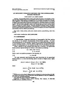
A laboratory prototype of the 12-switch (can be configured for 9-switch) converter was designed and built; its photograph is shown in Fig. 7. The gate PWM signals were generated using a dSPACE ds1104 real-time controller. The 12switch converter supplies three independent three-phase RL loads with the same nominal parameters as those used in the simulations. The switching frequency of the inverter is set to 1 kHz and the input DC is 50 V DC. The inverter dead time is approximately 8 µs. Illustrative waveforms of line voltage and phase voltages, phase and input DC currents are shown in Figs. 8a–8c. Even though the aforementioned experimental waveforms show some spikes especially that of Inv3 (25 Hz) in Fig. 8c, by and large, the waveforms show strong correspondence between simulations and experiments comparing the respective figures. The experiments thus validate the proposed method.
80 14 60 12 Amplitude
Idc [A]
40 20
5 Conclusions
10 8
0 6 −20 4 −40 2 −60 0.03
0.04
0.05 0.06 Time [secs]
0.07
0
0
200
400 600 800 1000 1200 Freq [Hz])
(c) Figure 6: 12-switch simulated waveforms for Inv1, Inv2 and Inv3: (a) phase a voltages (Inv1: top, Inv2: middle, and Inv3: bottom), (b) phase currents (Inv1: top, Inv2:middle, and Inv3: bottom), and (c) input DC current and its harmonic spectrum.
The CBPWM method for the 12-switch converter has been proposed. To the best of the authors knowledge, the generalized neutral voltages for the converter have been derived for the first time in this paper and used as the offset voltages required by this topology to decouple the converter’s three outputs. Additionally, the neutral voltages can be used to modify the modulation schemes for various drive applications just by specifying the null voltages dwell time distribution. The proposed algorithm has been validated by both theoretical simulation and experimental results. The results show that the desired voltages have been correctly synthesized.
Unauthenticated Download Date | 7/8/16 4:05 PM
GCB-PWM Method for a 12-Switch Converter |
(a)
183
(b)
(c) Note: All currents have been scaled down by a factor of 100. Figure 8: Experimental waveforms: line voltage (Ch1), phase voltage (Ch2), phase current (Ch3), and input DC current (Ch4) for (a) Inv1; 95 Hz, (b) Inv2; 60 Hz, and (c) Inv3; 25 Hz respectively.
References
[3]
[1]
[4]
[2]
Jones, M., Vukosavic, S., Dujic, D., Levi, E., Wright, P.: Five-leg inverter pwm technique for reduced switch count two-motor constant power applications. IET Electric Power Applications 2(5) (September 2008) 275–287 Lim, C.S., Rahim, N., Hew, W.P., Levi, E.: Model predictive control of a two-motor drive with five-leg-inverter supply. IEEE Transactions on Industrial Electronics 60(1) (Jan 2013) 54–65
[5]
Matsuse, K., Kezuka, N., Oka, K.: Characteristics of independent two induction motor drives fed by a four-leg inverter. IEEE Transactions on Industry Applications 47(5) (Sept 2011) 2125–2134 Fernandes, D., Costa, F., dos Santos, E.: Digital-scalar pwm approaches applied to four-leg voltage-source inverters. IEEE Transactions on Industrial Electronics 60(5) (May 2013) 2022– 2030 Heydari, M., Varjani, A., Mohamadian, M., Fatemi, A.: Threephase dual-output six-switch inverter. IET Power Electronics 5(9) (November 2012) 1634–1650
Unauthenticated Download Date | 7/8/16 4:05 PM
184 | K. A. Aganah and O. Ojo [6]
[7]
[8] [9]
[10]
[11]
[12]
[13]
[14]
[15]
[16]
Dasgupta, S., Mohan, S., Sahoo, S., Panda, S.: Application of four-switch-based three-phase grid-connected inverter to connect renewable energy source to a generalized unbalanced microgrid system. IEEE Transactions on Industrial Electronics 60(3) (March 2013) 1204–1215 Dujic, D., Jones, M., Vukosavic, S., Levi, E.: A general pwm method for a (2n + 1) -leg inverter supplying n three-phase machines. IEEE Transactions on Industrial Electronics 56(10) (Oct 2009) 4107–4118 Kangarlu, M.F., Babaei, E.: Cross-switched multilevel inverter: an innovative topology. IET Power Electronics 6(4) (2013) Babaei, E., Kangarlu, M.F., Sabahi, M.: Extended multilevel converters: an attempt to reduce the number of independent dc voltage sources in cascaded multilevel converters. IET Power Electronics 7(1) (2014) 157–166 Kominami, T., Fujimoto, Y.: A novel nine-switch inverter for independent control of two three-phase loads. In: Industry Applications Conference, 2007. 42nd IAS Annual Meeting. Conference Record of the 2007 IEEE, IEEE (2007) 2346–2350 Oka, K., Matsuse, K.: A nine-switch inverter for driving two ac motors independently. IEEJ Transactions on Electrical and Electronic Engineering 2(1) (2007) 94–96 Liu, C., Wu, B., Zargari, N., Xu, D.: A novel nine-switch pwm rectifier-inverter topology for three-phase ups applications. In: Power Electronics and Applications, 2007 European Conference on, IEEE (2007) 1–10 Liu, C., Wu, B., Zargari, N., Xu, D., Wang, J.: A novel three-phase three-leg ac/ac converter using nine igbts. IEEE Transactions on Power Electronics 24(5) (May 2009) 1151–1160 Zhang, L., Loh, P.C., Gao, F.: An integrated nine-switch power conditioner for power quality enhancement and voltage sag mitigation. IEEE Transactions on Power Electronics 27(3) (March 2012) 1177–1190 Aganah, K., Karugaba, S., Ojo, O.: Space vector and carrierbased pwm modulation schemes for maximum utilization of voltage sources of a nine-switch converter. In: Energy Conversion Congress and Exposition (ECCE), 2012 IEEE. (Sept 2012) 2521–2528 Fatemi, A., Azizi, M., Shahparasti, M., Mohamadian, M., Yazdian, A.: A novel single-phase six-switch ac/ac converter for ups applications. In: Power Electronics, Drive Systems and Technologies Conference (PEDSTC), 2011 2nd , IEEE (2011) 408–414
[17] Dos Santos, E., Jacobina, C., da Silva, O.: Six-phase machine drive system with nine-switch converter. In: IECON 2011-37th Annual Conference on IEEE Industrial Electronics Society, IEEE (2011) 4204–4209 [18] Zhang, L., Loh, P.C., Gao, F., Blaabjerg, F.: A cascaded online uninterruptible power supply using reduced semiconductor. In: Energy Conversion Congress and Exposition (ECCE), 2011 IEEE, IEEE (2011) 3167–3172 [19] Divate, D., Bhosale, Y.: An improvement of power quality using nine-switch power conditioner with minimization of voltage sag. In: Electrical, Electronics and Computer Science (SCEECS), 2014 IEEE Students’ Conference on. (March 2014) 1–6 [20] Heydari, M., Varjani, A.Y., Mohamadian, M., Zahedi, H.: A novel variable-speed wind energy system using permanent-magnet synchronous generator and nine-switch ac/ac converter. In: Power Electronics, Drive Systems and Technologies Conference (PEDSTC), 2011 2nd , IEEE (2011) 5–9 [21] Liu, X., Wang, P., Loh, P.C., Blaabjerg, F.: A compact three-phase single-input/dual-output matrix converter. Industrial Electronics, IEEE Transactions on 59(1) (Jan 2012) 6–16 [22] Liu, X., Loh, P.C., Wang, P., Blaabjerg, F.: A direct power conversion topology for grid integration of hybrid ac/dc energy resources. IEEE Transactions on Industrial Electronics 60(12) (Dec 2013) 5696–5707 [23] Liu, X., Wang, P., Loh, P.C., Blaabjerg, F.: A three-phase dualinput matrix converter for grid integration of two ac type energy resources. IEEE Transactions on Industrial Electronics 60(1) (2013) 20–30 [24] Dehghan, S., Mohamadian, M., Yazdian, A.: Hybrid electric vehicle based on bidirectional z-source nine-switch inverter. IEEE Transactions on Vehicular Technology 59(6) (July 2010) 2641– 2653 [25] Gao, F., Zhang, L., Li, D., Loh, P.C., Tang, Y.: Optimal pulsewidth modulation of nine-switch inverter. In: Power Electronics and Drive Systems, 2009. PEDS 2009. International Conference on. (Nov 2009) 718–723 [26] Holmes, D.G., Lipo, T.A.: Pulse width modulation for power converters: principles and practice. Volume 18. John Wiley & Sons (2003) [27] Hava, A.M., Kerkman, R.J., Lipo, T.A.: Simple analytical and graphical methods for carrier-based pwm-vsi drives. IEEE Transactions on Power Electronics 14(1) (1999) 49–61
Unauthenticated Download Date | 7/8/16 4:05 PM