Tamkang Journal of Science and Engineering, Vol. 7, No 3, pp. 129-134 (2004)
129
Generally Applicable Self-masking Technique for Nanotips Array Fabrication Kuei-Hsien Chen1,2*, Chih-Hsun Hsu2, Hung-Chun Lo1, Surojit Chattopadhyay1, Chien Ting Wu1, Jih-Shang Hwang1, Debajyoti Das1 and Li-Chyong Chen2 1
Institute of Atomic and Molecular Science Academia Sinica Taipei, Taiwan 106, R.O.C. 2 Center for Condensed Matter Sciences National Taiwan University Taipei, Taiwan 106, R.O.C. E-mail:
[email protected]
Abstract Well-aligned nanotip arrays were fabricated via a self-masking dry etching technique in an electron cyclotron resonance (ECR) plasma process. Nanotip arrays of Si, poly silicon, GaN, GaP, sapphire, and Al were fabricated. Simultaneous etching of the substrate and formation of silicon carbide (SiC) protecting caps are attributed to the nanotip formation. The ultra-low turn on filed for electron field emission as well as the surface enhanced Raman Spectroscopic study of Si nanotips is also demonstrated. Key Words: Nanotip, Field Emission, Surface Enhanced Raman Spectroscopy.
1. Introduction Nano-scaled tips have been demonstrated for their unique properties much useful in different applications such as high-efficiency field emission [1], near-field optical microscopy [2], high-resolution atomic force microscopy and atomic-resolution scanning tunneling microscopy [3,4]. Recently a considerable attention has been focused on the potential and versatile applications of nano-tips e.g., in solar cells [5], optoelectronics [6] and bio/chemical sensing devices [7-9]. However, a number of crucial technological issues standing on the way of current nanotechnology to flourish farther, need to be solved urgently. Those include uncontrolled growth of nanotips and incompatibility of the nanofabrication process among its various steps and to the *Corresponding author
popular and well-established microfabrication techniques adopted by the semiconductor industry. Accordingly, an efficient nanofabrication process contributing to ultra fine and controllable geometric features over large area and universality in process technology for various materials with minimization in process-steps will significantly enrich nanotechnology to step forward. In this article, we report an one-step and selfmasked dry etching (SMDE) technique for fabricating uniform and high density nanotip arrays over a large area in a cost effective manner, using a commercial high-density electron cyclotron resonance (ECR) plasma reactor. In addition, the unique field emission (FE) property of Si nanotips and the relatively simple deposition of well-separated Ag nanoparticulates on Si nanotips are promising for the applications in the field emission devices and surface enhanced Raman spectroscopy (SERS) substrates.
130
Kuei-Hsien Chen et al.
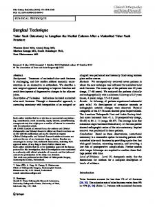
2. Fabrication and Applications of Nanotips 2.1. Generally Applicable Technique for Nanotips Fabrication Reactive gases comprised of argon (Ar), hydrogen (H2), methane (CH4), and silane (SiH4) were activated typically by a microwave power source at a chamber pressure of 5.8 mTorr, during the nanotip fabrication process. Nanotip arrays were etched from a variety of substrates maintained at a temperature between 100°C to 250°C, as measured by a two-color optical pyrometer. Figure 1 shows the tilted top-view high-resolution scanning electron microscope (HRSEM) images of nanotip arrays formed by the SMDE process on various substrates e.g., single-crystal silicon (Si), polycrystalline silicon (poly-Si), gallium nitride (GaN), gallium phosphide (GaP), sapphire and aluminum (Al) [10]. Nanotips were found to be well aligned and uniformly distributed
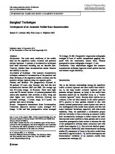
over the entire surface with a high density for all the samples. In case of single crystal Si wafers, nanotip density as high as 1.5 ´ 1011/cm2 over a large area of 6 inch in diameter was obtained with a high aspect ratio of ~ 50. Typical HRTEM images of the nanotips for crystalline silicon and GaP are shown in Figure 2A and 2B, respectively. In both cases, ~1 nm apex of the tip was obtained, which can be favorably compared to the finest tip reported so far. Moreover, caps at the apex are characterized as SiC, which holds the key for nanotips fabrication. Figure 3 illustrates the schematic of a model for the nanotip formation. The gas-mixture comprised of SiH4, CH4, Ar and H2 present in the ECR plasma, is supposed to react and play two different roles: formation of SiC nanomasks and etching of the substrate to develop nanotips (Figure 3A). It is believed that in the ECR plasma, SiC nano-sized clusters are formed from the reaction of SiH4 and CH4 plasma [11], and uniformly dis-
Figure 1. The tilted top-view HRSEM morphologies of the nanotip arrays fabricated by the self-masked process of various substrates.
Generally Applicable Self-masking Technique for Nanotips Array Fabrication
131
tributed over the substrate surface (Figure 3B). Meanwhile, Ar and H2 plasma are responsible for the physical etching and chemical etching, respectively, of the substrates. The SiC nanoclusters deposited on the substrate then act as the nano-masks, because of their higher hardness and chemical inertness, their etching rate is substantially less than that of the substrate materials. Under the protection of SiC nano-mask caps, formation of high density and high aspect ratio nanotip arrays can be realized (Figure 3C). Figure 2. The HRTEM image of the Si nanotip reveals a SiC cap formed on top of the tip. Inset shows the magnified HRTEM image of the interface between Si and SiC cap (similar feature is also observed in GaP case).
Figure 3. A schematic description of (A-C) the formation of the silicon nanotips by ECR plasma of reactive gases and (D) subsequent formation of the silver nanoparticulates by ion beam sputtering.
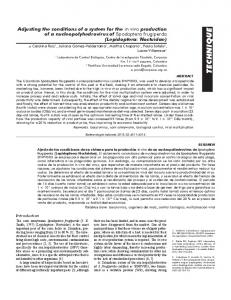
2.2. Field Emission of Nanotips with Ultra-Low Turn on Field Field emitters utilizing lithographically etched silicon tips usually require extremely small tip to gate spacing to achieve the required emission current density because of its high turn-on field of several tens of V/mm [12]. A gross reduction in tip diameter and increased packing density of the field emitter tips is required for a major advancement in this field [13]. Because of numerous useful applications of the silicon nanotip arrays as field emitters, the field emission property, in particular, has been extensively investigated. Figure 4 shows a typical field emission result for SiC capped nanotips on a p-type Si substrate. A high current density of 3.0 mA/cm2 at an applied field as low as ~1.0 V/m has been achieved. In the measurement the emission current was limited under 3.0 mA/cm2 as shown in the figure to avoid damaging the emitter tips. The FowlerNordheim plot depicted in the inset shows good linear relationship, indicating ideal field emission of the nano-
Figure 4. A typical field emission data obtained from silicon nanotips, demonstrating the ultra-low turnon electric fields. The inset presents the corresponding Fowler-Nordheim plot.
132
Kuei-Hsien Chen et al.
tips. The turn-on field for the nanotips, defined as the electric field required to extract a current density of 10 A/cm2 from the tip, is found to be ~0.35 V/m, which is much lower than other reported materials. Lowering of the operational voltage has multiple effects on the performance of the emitter arrays. The low voltage operation reduces the emitter driving input power and thereby maximizes the power gain and the emission efficiency of the device. In addition, low-voltage operation improves the transconductance of the emitter arrays for any given operating current. The total transconductance of the emitter array again increases effectively with the emitter packing density. Moreover, both smaller tip diameter and larger aspect ratios are advantageous in improving the field enhancement factor at the tip and thereby increasing the transconductance.
2.3. Surface Enhanced Raman Spectroscopy Study using Si Nanotips as Substrate Surface enhanced Raman spectroscopy (SERS) has evolved as a powerful and sensitive tool for detection and identification of a wide range of adsorbate molecules down to the limit of single molecule detection [13-16]. Using specially prepared rough metallic surfaces the otherwise weak Raman signals can be enhanced by several orders making detection possible [17]. This enhancement can be as large as 1014 [13]. Hence, SERS has the capability to unite the sensitivity of fluorescence with the rich structural content inherent to Raman spectroscopy. Here, we demonstrate a nanostructured substrate on which silver or gold nanoparticulates, with less than 10 nm diameter, can be self assembled at an extremely high density that readily exhibit the surface enhancement.
Figure 5. (A) Raman spectra of Rhodamine 6G drop coated on as-grown silicon nanotips (the concentration of Rhodamine 6G is marked on each curve); SERS spectra of different concentrations of Rhodamine 6G drop coated on silicon nanotips covered with different amounts of self assembled silver nanoparticulates, (B) 1 ´ 10-6 M, (C) 1 ´ 10-7 M, (D) ~ 1 ´ 10-10 M (the numbers mentioned on each curve in Figure 5 (B-D) denote silver sputtering times).
Generally Applicable Self-masking Technique for Nanotips Array Fabrication
These substrates are stable and reproducible as far as SERS signals of analytes are concerned. Assuming all the nanotips are touching each other at the bottom, the surface area can be quantified at 150 m2cm-3, which is as good as the high porosity porous silicon. These substrates were then coated with silver (Ag) by Argon ion beam sputtering (IBS) (Figure 1D) using silver target. Due to the surface energy difference between the silicon nanotips and that of the noble metals they self assembled to form nanoparticulates on these nanotips. The size of these nanoparticulates was always between 4-10 nm with a rather small departure from the mean value. The density of these particulates, under optimized IBS time, was also very high and could be found throughout the entire surface of the nanotips. Commonly used molecules for SERS experiments such as Rhodamine 6G and BPE were then dispersed by drop coating onto these substrates, in measured quantities, from their solution (in methanol) and dried. They were then used for the Raman measurements using a Renishaw-1000 micro Raman spectroscope. In the optimized condition, for 10 minutes IBS time, high density of monodisperse Ag nanoparticlulates could be obtained throughout the entire surface of these nanotips. This ensured a rather high density of nanoparticulates that could be packed over a unit area of the substrate in comparison to the flat silicon or other polymer substrates normally used for SERS. The density and dispersion of the metallic nanoparticulates could be controlled easily by the sputtering time only with little deviation in the particle size. This renders these substrates as ideal system for verifying theoretical modeling of SERS. Surface enhanced Raman signals of Rhodamine 6G (Figure 5) were collected from silicon nanotip substrates coated with 0 min (uncoated), 1 min, 3 min, 5 min, 10 min, and 20 min of silver using IBS (BPE also shows similar tendency). Different concentrations of Rhodamine and BPE were dispersed on these differently coated substrates. The intensities of the Raman signals were markedly higher for higher concentrations (10-6 M) of Rhodamine 6G used (Figure 5B) and merely visible for lower concentrations approaching 10-10 M (Figure 5D). This tremendous enhancement is attributed to several factors. The silicon nanotips with silver particulates were found to be hydrophilic whereas the silver coated flat silicon substrates were found to be hydrophobic in our experiments. The same volume of
133
analyte molecules dispersed uniformly over the whole surface area of the nanotip substrate reproducibly produced SERS spectra, whereas the same volume of analyte on the flat silicon substrate was confined to a small area only, outside which no SERS spectra could be obtained. Other than this, the particle size and inter-particle separation of silver particulates on the silicon nanotips would affect SERS activity.
3. Conclusion In conclusion, the fabrication of uniform nanotips on various substrates over large area at low temperatures has been demonstrated by this SMDE technique. Excellent field emission (3.0 mA/cm2 at ~1.0 V/m) from SiC-capped silicon nanotip arrays has been demonstrated, which opens up potentials for feasible field emission displays and vacuum electronic devices. The high density of the silicon naotips and a consequent uniform density of the metal nanoparticles, which can be controlled by the ion beam sputtering time of the metal targets, ensures high levels of inter and intra-substrate reproducibility. Molecules with concentrations as low as 10-10 M could be detected in a reproducible and stable fashion with the help of these substrates.
Acknowledgment The work is supported by Academia Sinica, the Ministry of Education and National Science Council. One of the authors, D. Das, is currently at Energy Research Unit, Indian Association for the Cultivation of Science, Calcutta, India.
References [1] Ravi, T. S.; Marcus, R. B.; Liu, D. J. Vac. Sci. Technol. B 1991, 9, 2733. [2] Williams, C. C.; Davis, R. C.; Neuzil, P. US patent 5,969,345 (1999). [3] Nishijima, H.; Kamo, S.; Akita, S.; Nakayama, Y. Appl. Phys. Lett. 1999, 74, 4061. [4] Cho, K.; Joannopoulos, J. D. Phys. Rev. Lett. 1993, 71, 1387. [5] Striemer, C. C.; Fauchet, P. M. Appl. Phys. Lett. 2002, 81, 2980. [6] Ponce, F. A.; Bour, D. P. Nature 1997, 386, 351.
134
Kuei-Hsien Chen et al.
[7] Lin, V. S. Y.; Motesharei, K.; Dancil, K. P. S.; Sailor, M. J.; Ghadiri, M. R. Science 1997, 278, 840. [8] Kovalev, D.; Timoshenko, V. Y.; Kunzner, N.; Gross, E.; Koch, F. Phys. Rev. Lett. 2001, 87, 68301. [9] Hickman, J. J.; Ofer, D.; Laibinis, P. E.; Whitesides, G. M.; Wrighton, M. S. Science 1991, 252, 688. [10] Hsu, C. H.; Lo, H. C.; Chen, C. F.; Wu, C. T.; Hwang, J. H.; Das, D.; Tsai, J.; Chen, L. C.; Chen, K. H. Nano Letters [Web published, 2004]. [11] Lee, W. H.; Lin, J. C.; Lee, C.; Cheng, H. C.; Yew, T. R. Diam. & Relat. Mater. 2001, 10, 2075. [12] Yomaoka, Y.; Goto, T.; Nakao, M.; Kanemaru, S.; Itoh, J. Jpn. J. Appl. Phys. 1995, 34, 6932. [13] Lo, H. C.; Das, D.; Hwang, J. S.; Chen, K. H.; Hsu, C.
H.; Chen, C. F.; Chen, L. C. Appl. Phys. Lett. 2003, 83, 1420. [14] Nie, S.; and Emory, S. R. Science 1997, 275, 1102. [15] Kneipp, K.; Yang, Y.; Kneipp, H.; Parleman, L. T.; Itzkan, I.; Dasari, R. R.; Feld, M. S. Phys. Rev. Lett. 1997, 78, 1667. [16] Xu, H.; Bjerneld, E. J.; Kall, M.; Borjesson, L. Phys. Rev. Lett. 1999, 83, 4357. [17] Fleishmann, M.; Hendra, P. J.; McQuillan, A. J. Chem. Phys. Lett. 1974, 26, 163.
Manuscript Received: Mar. 21, 2004 Accepted: May 20, 2004