Implementation of a BPSK Transceiver on Hybrid Software Defined Radio Platforms Yahia Tachwali
Hazem Refai
University of Oklahoma Department of Electrical & Computer Engineering 4502E 41st Bldg 4, Tulsa ,OK 74135
[email protected]
University of Oklahoma Department of Electrical & Computer Engineering 4502E 41st Bldg 4, Tulsa ,OK 74135
[email protected]
Abstract- Software defined radio (SDR) is an important element of wireless technology and fast becoming a hot topic in the telecommunication field. Determining the digital hardware composition of a software radio is a key design step in its creation. Hybrid GPP/DSP/FPGA architecture is a viable solution for software defined radio technology. This paper demonstrates a practical design and implementation procedure for a wireless digital modem on software defined radio platforms and reports a detailed description of the baseband signal processing logic design in the FPGA portion of it. Design verification is performed through hardware in the loop testing methodology. A framework for designing wireless digital modems on hybrid software radio platforms is discussed.
radio platforms . The digital transceiver is implemented using System generator for DSP® [9] for the implementation of FPGA blocks and SIMULINK® and Real Time Workshop® to develop DSP signal processing modules [10]. The paper is organized as follows. The hardware description of the software defined radio platform is presented in section 2. In section 3, we discuss the design partitioning between FPGA and DSP. A detailed design procedure in the FPGA portion of the design is reported in section 4. Section 5 lists experimental plots of the signal flow through the BPSK transmission and reception in FPGA. Finally, a conclusion is provided in section 6.
Keywords-FPGA; SDR; BPSK; Digital transceiver design
I. INTRODUCTION With the recent advent of software defined radio [1], wireless communication systems have become applicable solutions to a wider range of challenging applications. However, wireless communication standards require different computational complexities as shown in table 1 [2]. There are many silicon solutions for implementing various signal processing functions of digital radios. When selecting architectures for SDR applications, a combination of processing elements can achieve a balance in cost, power, performance, flexibility and reliability. Embedded signal processing systems generally use four types of advanced processing devices to execute digital signal processing: application specific integrated circuits (ASICs), field programmable gate arrays (FPGAs), general purpose processors (GPP) and digital signal processors (DSP) [3,4]. TABLE I COMPUTATIONAL COMPLEXITY OF SOME WIRELESS COMMUNICATION STANDARDS
Wireless standard 802.11 a&b WCDMA GPRS GSM
Approximate computational complexity (MIPS) 9000 6000 300 100
In this paper, a BPSK based digital wireless transceiver centered at 400 MHz on a GPP/DSP/FPGA based software radio platform [5] is used. While a number of digital radio implementations have been presented in the literature [6-8], most are conducted on a single processing engine such as FPGA [6,7] or DSP [8]. This paper provides a framework for designing wireless digital modems on hybrid software
Figure 1. Hardware block diagram of the software defined radio platform
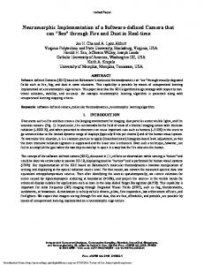
II. THE SOFTWARE RADIO PLATFORM The wireless transceiver is implemented using a modular small form factor (SFF) software defined radio (SDR) platform produced by Lyrtech. Figure 1 shows a simplified hardware block diagram of the SDR platform which consists of three modules: digital signal processing module, data conversion module and RF module. The digital transceiver design is implemented in the digital signal processing module. The other two modules are configurable through a number of control signals generated from the digital signal processing module. The digital signal processing module uses a Virtex-4 FPGA and DM6446 DMP. The DMP chip features an advanced Very Long Instruction Word (VLIW) DSP portion which is responsible for some signal processing tasks in the transceiver design, and a Reduced Instruction Set Computer
Authorized licensed use limited to: University of Oklahoma Libraries. Downloaded on March 23, 2009 at 17:05 from IEEE Xplore. Restrictions apply.
DAC ADC
Upconversion to IF Downconversion to BB
Pulse shaping
Interpolation Decimation
Match filtering
upsampling
Modulator (Mapping) Demodulator
Integrate & dump
Parallel to Serial Serial to Parallel
VPSS
Digital Signal Display
VPSS
Digital Signal Generation
(RISC) ARM9 core which is used for running a real-time operating system RTOS. The data conversion module is equipped with a 125 MSPS, 14-bit dual channel ADC and a 500 MSPS 16-bit dual channel interpolating DAC. It is equipped also with programmable gains at the input and output of the ADC and DAC respectively. This enables the implementation of automatic gain control AGC and transmission power control. The RF module is configured to have either 5 or 20 MHz bandwidth with transmission frequency range of 200-930 MHz and receiving frequency range of 30-928 MHz. The digital transceiver implementation in this paper is centered at 400 MHz which is within the optimum operation range of the available platform antennas. Interfacing between DSP and FPGA is achieved using different connections. The main bridge between the two processing engines is the Video Processing Sub-system (VPSS) data port, i.e. a DM6446 DSP 16-bit synchronous video data transfer port. The VPSS is composed of the video processing front end (VPFE) and the video processing back end (VPBE), where the VPFE is used as an input interface to the DSP and the VPBE as an output interface from the DSP. The VPSS was adapted to be used on the digital processing module of the SDR platform as an interface to transfer data other than video between DSP and FPGA. In order to emulate video signals, Vsync and Hsync signals are generated by the VPFE of FPGA interface. The FPGA VPBE uses the Vsync and Hsync signals generated by the DSP to synchronize the incoming data transfer. Also, another interfacing method is achieved by custom registers which are shared memory blocks of eight 32-bit words between DSP and FPGA On-Chip Peripheral Bus (OPB). Additional information about the hardware specification can be found in [5].
Upconversion to RF
Downconversion to IF
characteristics of each processing engine. While the distributed arithmetic principles associated with digital filter designs enable the parallel processing scheme in FPGA, algorithms that require sequential analysis and decision making such as synchronization and AGC are implemented on the DSP. The communication between FPGA and DSP is maintained through the two connection methods discussed earlier. For high speed data flow, the VPSS connection has been chosen. On the other hand, the shared custom registers were used to exchange data at low sampling frequency to be used for AGC or synchronization tasks. A block diagram of the complete BPSK transceiver is illustrated in Figure 2. The diagram shows the signal processing task partitioning between FPGA and DSP. IV. FPGA BASED IMPLEMENTATION The digital transceiver is comprised of transmitter and receiver stages that operate in duplex mode. At the same time the receiver stage represents the inverse data path of the transmitter, it also operates additional functionalities to maintain synchronization. While synchronization is an essential part of any digital receiver, discussing its design procedure is beyond the scope of this paper and is addressed instead in [11-13]. The transceiver is designed to transmit and receive signals in mobile communication environment. The signal is sampled at 24.414 kHz using PCM3008 Codec chip, which is often used for voice signals. Hence the design requirements have to comply to the operation environment and available hardware resources. Presently, the mobile communication environment is challenged from rapidly changing wireless channel characteristics caused primarily by mobility. Therefore, the signal to noise ratio of the wireless signal is expected to be low. Binary Phase Shift Modulation (BPSK) is chosen for this prototype because of its ability to tolerate low SNR values, as well as its simplicity, which is reflected in its low cost implementation. Also, the available codec in the platform defines the data rate required. For many digital communications, 10 bits appear to be sufficient for voice applications. As a result, the data rate of the digital transceiver should be 244.14 kbps using BPSK modulation. Based on the discussion above, we are now able to show the design procedure of a BPSK digital transceiver as shown in figure2.
Synchronization
A. Transmitter: AGC
DSP
Custom Registers
FPGA
Figure 2 BPSK transceiver block diagram
III. HARDWARE DESIGN PARTITIONING The BPSK transceiver is decomposed into different signal processing functions, which are distributed between FPGA and DSP. The partitioning was made based on the inherent
In the following sections, we are going to discuss the design procedure for each transmitter block. Figure 3 shows the transmitter logic design of BPSK transceiver.
• Parallel to serial The voice signal samples are represented by 10-bit words. This stage splits the input word into 10 time-multiplexed output words. The order of output bits (MSB or LSB first) should be considered for Serial to parallel and parallel to serial stages.
Authorized licensed use limited to: University of Oklahoma Libraries. Downloaded on March 23, 2009 at 17:05 from IEEE Xplore. Restrictions apply.
Figure 3 Transmitter logic design
• Modulator For BPSK, the modulator maps binary zeros and ones to –1 and 1 which are the normalized values of the maximum input range of the digital to analog converter. • Upsampling The number of samples per symbol is a design choice subject to a tradeoff between hardware cost and an elevated error rate. A relatively low number of samples per symbol relaxes the requirement of pulse shaping filter design but only at the expense of higher symbol error rate which results from fewer number of samples used to decide the symbol value. On the other hand, a high number of samples per symbol relaxes design specifications for a synchronization circuit, but increases the order of the pulse shaping filter to achieve the same frequency response. It has been shown that an upsampling ratio of 4 is the minimum ratio that enables PLL loops for frequency tracking [15]. However, for our prototype, a ratio of 8 was chosen as a balancing point between the two tradeoffs mentioned earlier. • Pulse shaping The pulse shaping filter used is a square root raised cosine filter. The excess bandwidth factor is 0.2. The order of the pulse shaping filter is an integer multiple of the upsampling factor (the order is 48 in this design). This allows the impulse response of the filter to span an integer number of symbols. An odd number of taps is used to allow the middle point of the impulse response to be at the peak position; this is beneficial for synchronization. The coefficients of the pulse shaping filters are scaled to avoid overflow in hardware. A generally accepted scale factor is given by [14] 1 (1) SF = ∑ h 2 (k )
(
)
Another practical method employed to avoid hardware overflow is scaling the coefficients so that the highest coefficient value will be as close as possible to 1 using a scaling factor (2^k) and applying a left shift operation of the filtering result (