International Journal of Computing and Digital Systems ISSN (2210-142X) Int. J. Com. Dig. Sys. 4, No.4 (Oct-2015) http://dx.doi.org/10.12785/ijcds/040409
Implementation of Efficient Parallel Prefix Adders for Residue Number System CH. Pavan Kumar1 and K.Sivani2 1, 2
KITS, Warangal, Telangana, India
Received 22 March 2015, Revised 1 July 2015, Accepted 20 August 2015, Published 1 October 2015 Abstract: In this paper we proposed a high speed and area efficient Kogge-stone, Ladner-fischer and Knowles adders by modifying the existing architectures by eliminating the redundant black cells. Currently the speed of the multipliers are restricted by the speed of adders for partial products addition. The major problem with the binary addition is the carry chain delay, to address this problem most of the modern adder architectures are implemented using parallel prefix adders. The delay of the parallel prefix adders are directly proportional to the number of levels in the carry propagation stage. Due to the logarithmic delay of the parallel prefix adders delay problems have effectively reduced. Kogge-stone is one of the fastest adders. We has eliminated the redundant black cells and performed re-routing thus minimizing the logic delay compared to the previous adders. Coded modified architecture in Verilog HDL, Simulated and synthesized using Xilinx ISE. Compared the modified architectures of Kogge-stone, Ladner-fischer & Knowles adders are found to be an improvement in the delay with the previous adders. Keywords: Kogge-stone adder, Knowles adder, Ladner-fischer adder, Gray cells, redundant black cell, Parallel prefix adders.
1. INTRODUCTION In various VLSI designs adders are most frequently used. The binary adder is the most important element in most digital circuit designs including digital signal processors (DSP), microprocessor data path units. In many applications of digital systems several types of adders can be used such as half & full adders, ripple carry adders, carry look ahead adders etc. Among all these adders Carry Look Ahead adder has an improved delay compared to half adder, full adder and ripple carry adder. The Carry Look Ahead (CLA) adder improves the speed by reducing the amount of time required to determine the carry bits. To propagate the carry to the next stages it introduced two new signals called Propagate and Generate (G, P).But the problem with the CLA is, as the number of input bits is going to be increased the delay of adder becomes worst. To eliminate this problem engineers devised new adders called Parallel prefix adders. The logarithmic delay of the parallel prefix adders improves the speed efficiently as well as requires less area requirements. The parallel prefix adders has found to be applicable in the various fields ranging from pseudorandom number system, cryptography[1],[2],[3],convolution computations without round-off errors[4],[5],[6].The residue number
system divides the number into parts (residues) and performs the addition in parallel without propagating carries, results in a significant speed up over the corresponding binary operations. The residue number System is best suitable for applications of digital signal processors [7], FIR filters and communication components offering less speed, low-power characteristics. The functioning of parallel prefix adders can be achieved in 3 stages. These parallel prefix adders precompute the carry to eliminate the carry propagation problems and reduce the delay of the adder. In the first stage carries are generated using two signals (G, P) in the White cell, here G is the carry bit of the half adder and P is the sum bit of the half adder. This stage is called as preprocessing stage. In the 2nd stage carries will be parallelizable to the next stages, so carry chain delay is reduced in this stage. This stage uses Black cell and Gray cell for computation of carries. This stage is called as carry look ahead stage. So 3rd stage generates the sum using the previous stage carries and propagates bits. Sum is generated by the Exclusive-OR operation of the previous carries and propagates bits. Buffers can be used in the last stage to propagate the carries to the sum generation stage. The output carry of the Black cell or
E-mail:
[email protected],
[email protected]
http://journals.uob.edu.bh
296
CH. Pavan Kumar: Implementation of Efficient Parallel Prefix…
Gray cell of the last stage is Cout =Gi. This stage is called as the post-processing stage. 2.
PARALLEL PREFIX ADDERS
A. Basic cells The delay problems have efficiently reduced by modifying the existing architecture of CLA, thus speeding up the propagation delay problems using parallel prefix adders. These adders are the parallel prefix form of the carry look ahead adder. The main advantage of the parallel prefix adders is that carry chain delay will be reduced as we go on increasing the number of bits from 8 to 16, 32, 64and 128 bits. The efficiency of the parallel prefix adders will be high even for the higher order input bits as compared to the carry look ahead adder. These adders results in logarithmic delay, so that the carries will be propagated to the next stages very speedily. B. GP Block This block is the first stage of the parallel prefix adder which pre-computes the carry by using two signals generate and propagate (G, P). Generate and propagate block takes a pair of inputs (a, b) and calculates generate and propagate bits using the following equations. A
B GP
g,p g= gi, & p= pi 3.
STAGES OF PARALLEL PREFIX ADDERS
This stage computes generate and propagate signals for each pair of inputs A and B. Pi=Ai XOR Bi
…..(1)
Gi=Ai AND Bi
…..(2)
A. Carry Generation Stage This stage computes the carries corresponding to each bit. Execution of these operations is carried out in parallel. After the computation of carries in parallel they are segmented into smaller pieces. We uses carry propagate and generate signals as intermediate signals which are given by the logic equations CPi:j = Pi: k +1 and Pk: j ….(3) CG i:j=Gi:k+1 or (Pi:k+1and Gk:j) .…(4) B. Post Processing Stage This is the final stage of all adders of this family which computes the sum bits. Ci-1= (Pi and Cin) or Gi …. (5) Si =Pi Xor Ci-1 …. (6)
g, p g= a.b; p= a XOR b; C. Black Cell The black cell takes the two pairs of input signals (gi, pi) and (gj, pj) and computes generate and propagate bits using the following equations. gi, pi
Buffer is uses the pair of input signals (gi, pi) and passes the same signals to the output. gi, pi
4.
TYPES OF PARALLEL PREFIX ADDERS
A. Kogge-Stone Adder
gj, pj BC g,p
g= gi+ pi .gj P=pi.pj D. Gray Cell This block takes two pairs of input signals (gi, pi) and (gj, pj) and generates the single output signal g. gi, pi
gj, pj GC g,p
g=gi+ pi.gj E. Buffer
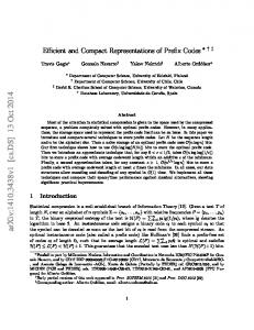
Figure 1. 8bit Kogge Stone Adder
http://journals.uob.edu.bh
Int. J. Com. Dig. Sys. 4, No.4, 295-300 (Oct-2015) The Kogge-stone adder is the parallel prefix form of the carry look ahead adder generates carries parallelizable to the next stages. The delay of the Kogge-stone adder is O (log2N).This is the most commonly used high-performance adder in the digital circuits. There are various types of parallel prefix adders such as Brent-Kung, Sklansky, Knowles and Ladner-fischer adders etc. Among all these adders it is found from literature that Kogge-stone adder is one of the best performance adder. In this paper we proposed 3 architectures of Kogge-stone, Ladner-fischer and Knowles adders by modifying the existing architectures by reducing the redundant black cells so as to get the better performance compared to the previous structures. Elimination of redundant black cells resulted in efficient delay and area requirements. The adder priority in terms of worst case delay is found from the experimental results that Ripple Carry, Carry Look Ahead, Carry select and Kogge-stone adder. This is due to the reduced stages of critical paths of all carry tree adders. The drawback of the Kogge-stone adder are high area requirements as compared to the other adders. The advantages of Kogge-stone adder are 1. It provides Low depth. 2. Minimal fan-out at each node (implies faster performance). B. Modified Kogge-stone adder The Kogge-stone adder shown in figure 2 is faster than the existing structure due to the elimination of redundant black cells, thus compensating the delay. This adder modified by reducing the redundant black cells and re-routing to compensate for the functionality of the adder.PG network of modified adder is shown in figure 2.
297
adder also provides logarithmic delay so as reduces time consumed for calculation of carries and propagates the carries to the next stages very fastly. Sklansky adder has minimum logic levels and uses less than Kogge-stone and Knowles prefix adders. But the problem with the Sklansky prefix tree is its high fan-out. Ladner-fischer prefix adder is proposed to
Figure 3. Ladner Fischer Adder
eliminate this problem. Ladner-fischer is a structure, between the Brent-kung and Sklansky prefix adders. The delay of this adder is log2N+. D. Modified Ladner- Fisher Adder
Figure 4. Modified Ladner Fischer Adder Figure 2. Modified Kogge Stone Adder
C. Ladner- Fisher Adder This is also a type of parallel prefix adder which reduces the delay as well as consumes less area. This
E. Knowles adder These types of prefix trees are having flexible architecture. Knowles prefix trees has the fan-out at each level to name their family members. These types of prefix trees trade of from depth and inter connect area. http://journals.uob.edu.bh
298
CH. Pavan Kumar: Implementation of Efficient Parallel Prefix…
This adder is bounded by minimum depth. This adder provides different fan-out at same logic level called as Hybrid logic. The black cells and gray cells used in the carry generation network are less in this adder as compared to the Kogge-stone and Ladner-fischer adders so that the area requirements of this adder are less. Knowles adder has the following advantages 1. Low depth and inter connect area. 2. These adders are bounded by Ladner-fischer (minimum depth) and Brent-Kung (minimum fanout) topologies.
5.
The Parallel Prefix adders described in the paper have modified by reducing the black cells so as to reduce the delay and to increase the performance of the adder .One of the important concept of all carry tree adders is that each gray cell and black cell has its own task in overall output. For example in the 2nd stage of modified KSA circuit the left generate bit is calculated only if bit 6 and 7 is present. It requires generate bits from bit 0 to 5,but the generate bit must be chosen from the path which gives reduced delay and produces effective sum from bit 0 to 5.instead the generate bit must be chosen from the bits 0 to 6,this does not affects the circuit. But the final generate bit from bit-i cannot take any generate bits higher than “i”, so the end result will be affected as we are included the generate bits higher than “i”. The above mentioned method is a good start but even we can improve the performance of the adder by removing the redundant black cells. Redundant black cells can be removed without any adverse consequences but it has to be properly compensated, if not the delay will be increased considerably. And this can be compensated by hanging the routing (wiring). Performing the routing in only 1st and the 2nd stages produced an improvement in speed but doing the same in all 3 stages of carry-generate network increases delay. 6.
Figure 5. Knowles Adder
F. Modified Knowles Adder
ROUTING TECHNIQUE USED FOR MODIFIED ADDERS
ELIMINATION OF REDUNDANT BLACK CELLS
Gray cells are required to compute the generate bit which results in output carry at the final stage of the adder so that gray cells cannot be removed at the final stage of adder. The removal of redundant cells gives different results, so all the cells cannot be removed. So the cells which are going to be removed should results in increased speed and less area perspectives. Analyzing the last stage of KSA gives a better understanding of the redundant cells. In the last stage there are no redundant cells so all of them has to be remained the same. In the 2nd stage there are 2 redundant cells 5:2 and 4:1 can be removed and this can be compensated by directly giving the output of the 5:4 and gray cell 3:0 to the gray cell 5:0 in the last black cell 4:1 is compensated by giving the black cell 4:3 and gray cell 2:0 to the gray cell 4:0 in the last stage. The two gray cells 2:0 & 3:0 takes generate bit from gray cell 1:0.
Figure 6.Modified Knowles Adder
7.
IMPLEMENTATION
To code the different tree adders we have used Verilog Hardware Description Language using structural
http://journals.uob.edu.bh
Int. J. Com. Dig. Sys. 4, No.4, 295-300 (Oct-2015)
299
modeling in Xilinx ISE simulator design suite 14.2.And all the simulation results are synthesized using Spartan-3 FPGA XC3S400 with the speed grade of 4. Components of Various Adders Architecture Kogge stone adder Modified Kogge stone adder Ladner fisher adder Modified Ladner fisher adder Knowles adder Modified Knowles Adder
Delay 14.678 ns 11.984 ns 12.210 ns 10.436 ns 10.206 ns 9.962 ns
Figure 9. Modified Ladner Fischer Adder Simulation Result
8.
Figure 7. Modified KSA Simulation Result
CONCLUSION
In this paper we have presented an innovative method to reduce delay by modifying the existing architectures of Kogge-stone, Ladner-fischer and Knowles adders by reducing the redundant black cells and by re-routing (wiring) we have found an increased speed of adders as well as reduced area constraints. Therefore these adders can be used in any VLSI circuits where speed is the main constraint. REFERENCES [1] X.Lai and J.L.Massey, “A Proposal for a New Block
Encryption Standard”, EUROCRYPT, D.W.Davies, ed., vol.547, pages 389-404, Springer, 1991 [2] R.Zimmerman et al., “A 177 Mb/s Very Large Scale
Integrated Circuits implementation of the International Data Encryption Algorithm,” IEEE j.Solid-state Circuits, vol.29, no.3, pages 303-307, March, 1994. [3] H. Nozaki et al.,”Implementation of RSA Algorithm Based
on Residue Number system Montgomery Multiplication”, Proceedings. Third Int’l Workshop Cryptographic Hardware and Embedded Systems, pages 364-376, 2001. [4] Y.Morikawala, H.Hamada, and K.Nagayasu,”Hardware Figure 8. Modified Knowles Adder Simulation Result
Realization of High Speed Butterfly for the Maximal LengthFermatNumberTransform”, Transactions.IECE, vol.j66-D, no.1, pages 81-88, 1983.
http://journals.uob.edu.bh
300
CH. Pavan Kumar: Implementation of Efficient Parallel Prefix…
[5] M.Benaissa,
S.S.Dlay, and A.G.J.Holt,”CMOS VLSI Design of a High-Speed Fermat Number Transform Based Convolver/Correlator Using Three-Input Adders”, Proceedings IEE, vol.138, no.2, pages 182-190, April 1991.
[6] V.K.Zadiraka
and E.A.Melekhina ,”Computer Implementation of Efficient Discrete-Algorithms”, Cybernetics and systems analysis,vol.30,no.1,pages 106114,January 1994.
[7] H.T. Vergos and C. Efstathiou, “Efficient Modulo 2n+1
Adder Architectures,” Integration, the VLSI J., vol. 42, no. 2, pp. 149-157,Feb. 2009. [8] A. Hiasat, “High-Speed and Reduced Area Modular Adder
Structures forRNS,” IEEE Trans. Computers, vol. 51, no. 1,pp. 84-89, Jan. 2002. [9] C. Efstathiou, H.T. Vergos, and D.Nikolos, “Fast Parallel-
Prefix Modulo 2n+1 Adders,” IEEE Trans. Computers, vol. 53, no. 9,pp. 1211-1216, Sept. 2004. [10] H.T. Vergos and C. Efstathiou, “A Unifying Approach for
Weighted and Diminished-1 modulo 2n+1 Addition,” IEEE Trans.Circuits and Systems II, vol. 55, no. 10, pp. 10411045, Oct. 2008. [11] A. Hiasat, “High-Speed and Reduced Area Modular Adder
Structures forRNS,” IEEE Trans. Computers, vol. 51, no. 1,pp. 84-89, Jan. 2002. [12] C. Efstathiou, H.T. Vergos, and D.Nikolos, “Fast Parallel-
Prefix Modulo 2n+1 Adders,” IEEE Trans. Computers, vol. 53, no. 9,pp. 1211-1216, Sept. 2004. [13] H.T. Vergos and D. Bakalis, “On the Use of Diminished-1
Adders for Weighted Modulo 2n+1 Arithmetic Components,” Proc. 11th Euromicro Conf. Digital System Design, pp. 752-759, Sept. 2008.
Chinnala pavan kumar (M'12) was born in Warangal, Telangana, india in 1989. He received B.Tech degree in Electronics and Communication engineering from Jawaharlal Nehru Technological University Hyderabad, India, and the M.Tech degree in VLSI system design from Jawaharlal Nehru Technological University Hyderabad, India, in 2009 and 2011, respectively. Currently, he is pursing the Ph.D. degree in Jawaharlal Nehru Technological University Hyderabad, Telangana, India. He has been an Assistant Professor with the Department of Electronics and Communication engineering in Kakatiya Institute of Technology and Science, Warangal, since June 2013. He was an Assistant Professor with the Department of Electronics and Communication engineering, Vaagdevi Engineering College, Warangal, from 2011 to 2013. His current research interests include VLSI design, Ultra Low Power Designs and Sub threshold region modelling.
Kosaraju Sivani (M'12) was born in 1966. She received the B.Tech. Degree from Kakatiya University, Warangal, Telangana, India, the M.Tech. degree from the National Institute of Technology, Warangal, Telangana, India, and the Ph.D. degree from Jawaharlal Nehru Technological University, Hyderabad, Telangana, India. She is currently a Professor of electronics and instrumentation engineering at Kakatiya Institute of Technology and Science, Warangal, Telangana, India. Her current research interests include VLSI design and biomedical engineering.
http://journals.uob.edu.bh