Improving MLC PCM Performance Through Relaxed Write and Read for Intermediate Resistance Levels SAEED RASHIDI, Sharif University of Technology MAJID JALILI, Sharif University of Technology HAMID SARBAZI-AZAD, Sharif University of Technology & Institute for Research in Fundamental Sciences (IPM) Phase Change Memory (PCM) is one of the most promising candidates to be used at main memory level of the memory hierarchy due to poor scalability, considerable leakage power, and high cost/bit of DRAM. PCM is a new resistive memory which is capable of storing data based on resistance values. The wide resistance range of PCM allows for storing multiple bits per cell (MLC) rather than a single bit per cell (SLC). Unfortunately, higher density of MLC PCM comes at the expense of longer read/write latency, higher soft error rate, higher energy consumption and earlier wear-out compared to the SLC PCM. Some studies suggest removing the most error prone level to mitigate soft error and write latency of MLC PCM, hence introducing a less dense memory called Tri-Level memory. Another scheme, called M-Metric, proposes a new read metric to address soft error problem in MLC PCM. In order to deal with the limited lifetime of PCM, some extra storage per memory line is required to correct permanent hard errors (stuck-at faults). Since the extra storage is used only when permanent faults occur, it has a low utilization for a long time before hard errors start to occur. In this paper, we utilize the extra storage to improve the read/write latency in a 2-bit MLC PCM using a relaxation scheme for reading and writing the cells for intermediate resistance levels. More specifically, we combine the most time consuming levels (intermediate resistance levels) to reduce the number of resistance levels (making a Tri-Level PCM) and therefore improve write latency. We then store some error correction metadata in the extra storage section to successfully retrieve the exact data values in read operation. We also modify Tri-Level PCM cell to increase its read latency when M-Metric scheme is used. Evaluation results show that the proposed scheme improves read latency by 57.2%, write latency by 56.1%, and overall system performance (IPC) by 26.9% over the baseline. It is noteworthy that combining the proposed scheme and FPC compression method improves read latency by 75.2%, write latency by 67%, and overall system performance (IPC) by 37.4%. CCS Concepts: • Information systems → MLC PCM; • Hardware → Dense main memory; Additional Key Words and Phrases: Tri-Level PCM, M-Metric, write speed, read latency, energy consumption ACM Reference format: Saeed Rashidi, Majid Jalili, and Hamid Sarbazi-Azad. 0. Improving MLC PCM Performance Through Relaxed Write and Read for Intermediate Resistance Levels. ACM Transactions on Architecture and Code Optimization 0, 0, Article 0 ( 0), 31 pages. https://doi.org/0000001.0000001 Author’s addresses: S. Rashidi and H. Sarbazi-Azad, HPCAN Lab, Computer Engineering Department, Sharif University of Technology, Tehran, Iran; emails:
[email protected],
[email protected]; H. Sarbazi-Azad, School of Computer Science, Institute for Research in Fundamental Sciences (IPM), Tehran, Iran; email:
[email protected].; M. Jalili is now at University of Texas at Austin, Texas, USA; email:
[email protected] . Permission to make digital or hard copies of all or part of this work for personal or classroom use is granted without fee provided that copies are not made or distributed for profit or commercial advantage and that copies bear this notice and the full citation on the first page. Copyrights for components of this work owned by others than the author(s) must be honored. Abstracting with credit is permitted. To copy otherwise, or republish, to post on servers or to redistribute to lists, requires prior specific permission and/or a fee. Request permissions from
[email protected]. © 0 Copyright held by the owner/author(s). Publication rights licensed to Association for Computing Machinery. XXXX-XXXX/0/0-ART0 $15.00 https://doi.org/0000001.0000001 ACM Transactions on Architecture and Code Optimization, Vol. 0, No. 0, Article 0. Publication date: 0.
0:2
1
S. Rashidi et al.
INTRODUCTION
With increasing number of cores and developing sophisticated applications in today’s computer systems, larger main memory capacity is increasingly demanded. The large capacity of main memory results in less page faults and more application parallelism. Unfortunately, DRAM cannot satisfy the increasing demand for larger main memory capacity due to its power and scalability limits that makes further scaling of DRAM infeasible [31]. Therefore, emerging memory technologies have been proposed to be used in the main memory level of memory hierarchy. Phase Change Memory (PCM) is an emerging memory that is a candidate for replacing DRAM technology. A PCM device consists of Chalcogenide material (GST), capable of changing its resistance. Therefore, PCM stores data based on its GST resistance level. Compared to DRAM, PCM is more scalable [44] and denser, and consumes less standby power. The large resistance range of GST material allows for considering more than two resistance levels that lead to storing multiple bits per cell (known as MLC) and creating even more denser PCM memories. However, utilizing MLC PCM has several challenges. In the presence of multiple resistance levels, the write operation should be performed in a more exact way. Therefore, MLC write operation is performed using multiple Program and Verify (P&V) iterations that result in longer write latency and higher energy consumption. In addition, writing to the intermediate resistance levels in MLC PCM requires more non-deterministic number of iterations [26, 36]. PCM cells also suffer from a limited lifetime, and extra storage per line can greatly help to tolerate cells failure. However, this extra storage is not utilized for a long time before the line faces first permanent faults [17, 39]. Another drawback of MLC PCM is its vulnerability to resistance drift, that is changing cell value based on increasing cell resistance over time. A recent study [51] proposed Tri-Level PCM to use three resistance levels (instead of four levels in a 2-bit MLC PCM) to increase the reliability and write speed. In Tri-Level PCM, the most vulnerable resistance level of MLC PCM to drift (i.e. the third level) is removed, leaving a wide resistance region between the second and fourth resistance levels. This allows the 3 remaining levels be read much more reliably; it also reduces the write latency in Tri-Level PCM. Authors in [48] proposed to use a non-resistance metric (M-Metric) for determining cell value. In M-Metric, a linear voltage ramp is applied to determine the time that takes the cell to see a predefined reference current I R level. Cell values are differentiated by the time they require to converge to I R . In this technique, read latency is determined by the highest reference resistance (the resistance that differentiate the two highest resistance levels). M-Metric shows significant tolerance to resistance drift. Therefore, by using M-Metric, the soft error rate due to drift is significantly decreased making M-Metric a suitable approach as a read mechanism, although it increases the average access latency. To address the challenges of MLC PCM while exploiting its density, in this paper, we propose a morphable MLC/Tri-Level PCM architecture that enjoys the speed and reliability of Tri-Level PCM and the capacity of MLC PCM. More precisely, we make the following contributions: • We propose slight modification on the read mechanism of previously proposed Tri-Level PCM to boost its read speed compared to MLC PCM (Section 2.2.1). This is done by leveraging the vast region between two highest resistance levels in Tri-Level PCM to reduce the highest reference resistance, while reliability requirements are met. Using this new design, in the proposed morphable memory architecture using M-Metric read mechanism, the memory lines stored in Tri-Level mode can be read much faster than those kept in MLC mode. • We propose Relaxed Write/Read (RWR) to improve the write latency of MLC PCM by merging the intermediate resistance levels ("01" and "10") to one level (i.e. making it Tri-Level), and ACM Transactions on Architecture and Code Optimization, Vol. 0, No. 0, Article 0. Publication date: 0.
Improving MLC PCM Performance
0:3
use the unutilized hard error recovery storage to determine the exact value of the cells with intermediate resistance levels. To be more specific, in this method, instead of writing the exact values of intermediate state levels of MLC cells, they are written to the intermediate state level of Tri-Level cells, making them approximate. A simple mapping scheme is used to map each approximate cell to a single correction bit in unutilized part of the extra storage section. The mapped bits in unutilized part then determine the exact values of the approximate cells in read operation. This way, the write latency of MLC PCM is significantly decreased while the capacity of MLC PCM is maintained. We also show that RWR method has a positive impact on energy consumption and lifetime of MLC PCM. The objective of this paper is to provide a PCM main memory that has the capacity density of MLC PCM with much better access latency and reliability than the conventional MLC PCM. 2
PRELIMINARIES
There are several challenges in exploiting MLC PCM for mass production. In comparison with SLC PCM, the MLC write operation must spend more cycles to finish since there are a couple of intermediates states to be programmed. Basically, there are two types of write pulses in MLC PCM; SET and RESET. A RESET pulse is a short and high-power pulse that drives the cell’s temperature above its melting point and then quench its temperature quickly. This results in a larger amorphous region and thus, increasing the resistance of the cell. The SET pulse is a long and moderate-power pulse that gradually shrinks the amorphous region and hence decreases its resistance. Figure 1 shows typical SET and RESET write pulses. To cope with the difficulty of write operation in MLC PCM, the Program and verify method (P&V) is proposed in [36]. The write operation is divided into multiple P&V iterations. After each iteration, the resistance of the cell is examined, if it is in the desired resistance range, the write operation is finished; otherwise more P&V iterations are applied. Another issue is the limited write endurance of PCM cells; that is after a certain number of writes the cell will permanently stuck at a constant value, no matter which write pulse is applied to. After each write, a comparison read is required to ensure that the data were correctly written [17, 47]. Faulty cells are detected if the checking read returns unequal data with respect to the written data. To deal with this limitation, typically an extra storage per line is required to cover such permanent cell failures. Typically, the acceptable amount of storage overhead is 12.5%. For example, for 512-bit lines (a typical line size in PCM), 64-bit storage overhead is reserved to deal with such errors. Different methods like [17, 47, 50] try to use this storage in different ways to cover more stuck-at faults. One of the major concerns related to PCM is soft error caused by resistance drift; that is increasing the resistance value over time. According to study in [22], the drift could be modeled as: t Rdr if t (t) = R × ( )α (1) t0 In Equation 1, R is the initial resistance of the cell after programming, Rdr if t (t) is the resistance of the cell after time t. t 0 is the normalization constant that is usually equal to 1, and α is the drift exponent. Drift exponent has a normal distribution of N (µ α , σα2 ) for each state. It is observed that drift exponent is proportional to initial resistance (i.e. R 0 ), that means higher R 0 leads to higher α. Thus, special care must be taken to deal with resistance drift problem. One common way is to use scrubbing mechanism, that is periodically rewriting the lines to prevent further increase of cells resistance. Scrubbing comes at the cost of more traffic, energy consumption and earlier wearout. Therefore, the memory system must be designed in a way that be reliable enough to let the scrubbing period be postponed in order to mitigate its overhead. ACM Transactions on Architecture and Code Optimization, Vol. 0, No. 0, Article 0. Publication date: 0.
0:4
S. Rashidi et al. Table 1. MLC resistance distribution parameters. LoдR
State level Data 0 (Reset) 1 2 3 (Set)
Target(µ R )
00 01 10 11
6.00 4.74 3.8 3
Deviation(σ R )
0.098
α
Range (3σ R )
0.295
Sensing Margin R drift Margin
0.47 0.16 0.01
0.2
Mean (µ α )
Deviation (σ α )
0.1 0.06 0.02 0.001
0.4×µ α
Resistance distribution of different states follow normal distribution N (µ R , σR2 ). In this paper, we use the resistance distribution adopted from previous studies [20, 28]. Figure 2 shows the resistance bands of different states. Typically, the resistance domain is divided into three regions: target resistance band, drift margin region and sensing margin. The target resistance band is the desired resistance range that needs to be obtained after cell programming. Here, the target resistance band is set to be µ R ± 3σR . The drift margin accounts for dealing with resistance drift problem. As stated before, the resistance of the cell is increased over time; thus for each state a safety margin (drift margin) is needed to let the resistance be safely increased while read is still realized correctly (as long as resistance does not pass drift margin). In order to address the noise in read circuit, the sense margin is required [20]. In read operation, the resistance of the cell is compared to the reference resistances (i.e. usually the middle of sense margins) to determine which state the cell belongs to. Table 1 presents the parameters associated with distribution of figure 2. Note that the parameters in Table 1 are based on [28].
MQ
Current
RESET SET
Time
Fig. 1. SET, RESET, and moderate-quenched (MQ) pulses for programming intermediate states in MLC and Tri-Level PCM.
2.1
% of Cells
Text Text Text Text Text Text
11
3
Sense Margin
10
3.8
01
4.74
Drift Margin
00
6
LogR
Fig. 2. MLC Resistance distribution
Write Model
2.1.1 MLC Write Model. In MLC PCM, programming a cell to "00" and "11" states (or SET or RESET states) is done using a fixed number of iterations, but programming to intermediate states ("01" and "10" states) requires a number of non-deterministic P&V iterations. Because of the process variation and nondeterministic characteristics of PCM devices, the number of P&V iterations is cell-dependent. Even for the same cell the number of required iterations varies [26]. Thus, different approaches have been proposed to model P&V based write operation [26, 41, 46]. In this paper, we adopt the write model presented in [46], and assume that intermediate states require 4.05 P&V iterations, on average, to be programmed, as reported in [36]. The detailed description of the model is presented in Appendix A. To conclude the write scenario in MLC, Figure 3a shows the write operation for different states. As can be seen, the programming operation begins with a RESET pulse. A RESET pulse is enough ACM Transactions on Architecture and Code Optimization, Vol. 0, No. 0, Article 0. Publication date: 0.
Improving MLC PCM Performance 1
2
Non-Detrministic
0:5 3
Non-Detrministic
11: Reset
Set
10:
Reset
Set
Set
Set
01:
Reset
Set
Set
Set
4
1
L0: L1: L2:
00: Reset (a) MLC PCM write scenario
Reset MQ
2 Set MQ
Reset
(b) Tri-Level PCM write scenario
Fig. 3. Required write pulses for writing different values in MLC and Tri-Level PCM
for writing "00" data. By applying one SET pulse, the "11" data is written. But, for intermediate states (i.e. "01" and "10"), variable number of SET pulses should be applied for write operation. 2.1.2 Tri-Level Write Model. As stated before, MLC PCM suffers from several drawbacks. Recent studies at [51] showed that the drift problem might be so sever to make MLC PCM infeasible. Thus, they proposed to remove the most vulnerable resistance level to drift, that is the third-level. By removing the third level, the reliability of PCM is improved. It is clear that removing a level will decrease the storage density. By using the coding technique discussed in [51], two Tri-Level cells could store 3 bits, and consequently the density of Tri-Level becomes 1.5 bits per cell. Moreover, since the third level is removed, the write operation to the intermediate state can be done using a single pulse [51]. By applying the moderate-quenched (MQ) programming pulse (proposed in [27]), the write operation to intermediate state is done with 1 iteration in most cases. Figure 1 shows the MQ pulse. It is a RESET pulse with controlled falling slope. According to the study in [51], the latency of MQ pulse is less than SET pulse. This makes the latency of Tri-Level PCM close to SLC write latency. One drawback of MQ programming is its less precision compared to P&V method [27, 51]. To analyze the distribution change due to MQ programming, we used the similar method used in[51]. Table 2 presents the associated parameters of Tri-Level PCM. As shown in the table, σR of intermediate state is worsened from 0.098 to 0.110 and µ R is increased from 3.8 to 4.042. The mean drift exponent also is increased from 0.02 to 0.0269. Here, we redefine the resistance regions in a Tri-Level cell to improve its read/write latency. Since µ R is increased, we increase the target resistance band of intermediate state from 3σR to 4.8σR . This results in 100-1.5867E-04% success rate for write operations to intermediate state to be finished in only 1 iteration. For the remaining 1.5867E-04% of writes, another MQ iteration is required which is negligible. Thus, a verification step is required to see if the first MQ iteration is successful. Note that this verification step is not an overhead of MQ programming, since after each iteration the cell value must be checked for detecting stuck-at faults. We also set the drift margin of the intermediate state to 0.13. Later, we will show that this amount of drift margin is sufficient to meet reliability requirements (discussed in Section 2.3). Unlike the original Tri-Level PCM design in[51], we also decrease the reference resistance between second and third levels from 5.605 to 4.80. Decreasing the last reference resistance leads to improving the read latency as discussed in Section 2.2. As Tables 1 and 2 show, the first level of MLC PCM and first level of Tri-Level PCM, the fourth level of MLC PCM and third level of Tri-Level PCM are equal in terms of resistance distributions. Figure 3b shows the write scenario of Tri-Level PCM. Writing to the first and third level is the same as MLC PCM, but for writing to intermediate state, the MQ iteration is applied. ACM Transactions on Architecture and Code Optimization, Vol. 0, No. 0, Article 0. Publication date: 0.
0:6
S. Rashidi et al. Table 2. Tri-Level resistance distribution parameters.
State level L2
LogR Target(µ R )
Deviation (σ R )
Range (σ R )
6
0.098
0.295(3σR ) 0.528 (4.8σR ) 0.295(3σR )
L1
4.042
0.110
L0
3
0.098
2.2
α Sensing Margin
0.2
R drift Margin
Mean (µ α )
-
0.1
0.13
0.0269
0.01
0.001
Deviation (σ α )
0.4µ α
Read Model
Conventional read mechanism (called R-Metric) has serve vulnerability to resistance drift (R-metric is described in Appendix B). As a result, a recent study [48] proposed to use a less-sensitive read metric to drift, called M-metric. In M-metric, the cell is biased to a constant reference current (I R ) and the voltage across the cell is measured. In order to bias the cell to I R , authors in [37, 48] proposed to apply a linear voltage ramp to the cell. Consequently, the time that takes the cell to converge to I R determines the cell state, because the higher resistance leads to longer time to converge to I R . Figure 4 explains the read process. Figure 4a shows a linear voltage ramp that is applied to the cell. Figure 4b shows the MLC read process. The 3 curves in Figure 4b are reference resistance curves of MLC PCM. According to Figure 4b, if the cell gets to I R between 0 and t 1 , its content is interpreted as "11". If this time is between t 1 and t 2 , it shows "10", and if it is between t 2 and t 3 , its value represents "01". If the cell does not get to I R by t 3 , then its value is assumed to be "00". Therefore, in this method, the read latency is determined by the highest reference resistance value. Since in Tri-Level PCM the highest reference resistance value is decreased from 402K Ω to 63K Ω, the read latency is dramatically decreased. 2.2.1 Proposed M-Metric Read Mechanism. In the original Tri-Level PCM design [51], authors assumed parallel reads using R-metric mechanism; therefore, they assumed the read latency of Tri-Level PCM is the same as SLC PCM. However, in addition to vulnerability of R-Metric to drift, parallel reading is a costly technique in terms of hardware overhead and sensing current [19]. By using M-Metric, both MLC and Tri-Level PCMs could be reliably used. Moreover, increased reliability of Tri-Level PCM compared to MLC PCM makes it possible to decrease the last reference resistance value in M-Metric, hence the read speed in Tri-Level PCM is improved. Figure 4c shows the Tri-Level M-Metric reading process, with the same mechanism used in MLC PCM. Note that in Tri-Level PCM, there are two resistance references. The reference current is set to be I R = 1µA [37, 48]. According to [48], by applying a voltage ramp with a slope of Kslope , the time that takes the cell to get to I R is given by: 2KTu Ae f f
Ec −E f
I R τ0e kT M(I R ) = arcsinh[ ] q∆ZKslope 2qπr E2 e f f NT ∆Z
(2)
where q is the elementary charge, τ0 is the characteristic attempt-to-escape time for a trapped electron, ∆Z is the mean inter-trap distance, NT is the trap density, K is the Boltzmann constant, T is the temperature, and Ea = Ec − E f is the activation energy. r Ee f f is the effective bottom electrode radius and u Ae f f is the effective amorphous thickness. Both r Ee f f and u Ae f f are functions of PCM amorphous thickness, u A . Figure 5a shows a PCM device with indicated amorphous thickness (u A ). Figure 5b shows the relationship between u A ,r Ee f f and u Ae f f . ACM Transactions on Architecture and Code Optimization, Vol. 0, No. 0, Article 0. Publication date: 0.
Improving MLC PCM Performance
0:7
V(mV)
20 15 10 5 0 5 10 15 20 25 30 35 40 45 50 55 60 65 70 75 80 85 90 95 100 105 110 115 120 125 130 135 140 145 150 155 160 165
0
T(ns) (a) Linear voltage ramp with Kslope = 105 IR 1
I(µA)
0.9 0.8 0.7 0.6 0.5 0.4 0.3 0.2 0.1 0
165ns (132clk)
6.25ns(5clk) Rref3
Rref2 Rref1
13.75ns(11clk) 0
20
40
60
80
100
120
140
160
180
T(ns)
(b) MLC PCM read scheme.
I(µA)
IR 1 0.9 0.8 0.7 0.6 0.5 0.4 0.3 0.2 0.1 0
6.25ns(5clk)
Rref1
Rref2
30ns(24clk) 0
20
40
60
80
100
120
140
160
180
T(ns)
(c) Modified Tri-Level PCM read scheme.
crystal amorphous
uA
uAeff(nm)
Row Decoder
Column Decoder
50
50
40
45 40
30
35
20
uAeff
10
rEff
25
0
20
1
(a) Amorphous thickness, u A , of a PCM cell.
30
reff(nm)
Fig. 4. Timing details of M-metric read in MLC PCM and proposed M-metric read for Tri-Level PCM.
4
7 10 13 16 19 22 25 28 31 34 37 40 43 46 49 uA(nm)
(b) r Ee f f and u Ae f f curves as a function of u A .
Fig. 5. Amorphous (mushroom) thickness parameters of PCM.
We consider Kslope = 105 . Therefore, by using Equation 2, the sense latency of MLC PCM and Tri-Level PCM is 165ns and 30ns, respectively 1 . 1 Note
that according to study in [48], in Equation 2, the resistance of crystal part is assumed to be negligible compared to amorphous part, hence it is ignored. But at low resistances, the crystal resistance matters. Therefore, we have taken into account the crystal resistance by assuming R c r ys t al = 500Ω, since the lowest resistance in our distribution is around 500Ω. ACM Transactions on Architecture and Code Optimization, Vol. 0, No. 0, Article 0. Publication date: 0.
0:8
S. Rashidi et al.
The predominant impact of temporal drift is growth in activation energy (Ea ). In Equation 2, M is a weakly affected by activation energy (Ea ). According to study in [48], the drift exponent of M-Metric is an order of magnitude less than R-Metric. Applying a linear voltage ramp is a convenient and low cost method that simplifies the read circuit logic. In read operation, the current through the cell needs to be compared with I R . At certain times, the read circuit checks if the cell has reached I R and therefore determines the cell state. However, one drawback of linear voltage ramp is that its latency is determined by the reference resistances, meaning if the resistance range increases, the latency is increased as well. In this case, increasing the ramp slope or using a nonlinear voltage ramp may reduce the latency [37, 48]. However, in the range of interest (1K Ω − 1M Ω), the linear voltage ramp gives reasonable read latency for MLC PCM, hence we use this method for our read operation. 2.3
Reliability Model
The probability of soft error rate (SER) should be calculated in order to determine the scrubbing period. SER is the probability for a cell to change its state due to resistance drift. Since the resistance of the cell is permanently increased due to drift, the scrubbing operation is needed eventually. The scrubbing period should be determined in a way that makes its overhead low while keeping the SER low. Since we use M-Metric for determining cell state, resistance drift turns into M-Drift. According to [48], M-Drift could be modeled in a same way as resistance drift by: t Mdr if t (t) = M × ( )α M t0
(3)
where α M is the drift exponent of M-Metric. Here, we assume the mean value of drift exponent in M-Metric (µ α M ) to be 17 of R-Metric(µ α ), as reported in [5, 55]. In order to determine the SER, first the resistance distribution of MLC PCM (Table 1) and TriLevel PCM (table 2) should be converted to M distribution. By using Equations 5b and 2, the M distribution is calculated and presented in Table 3. Table 3a shows the M distribution of MLC PCM and Table 3b shows that for the Tri-Level PCM. It can be seen in Table 3 that the normal distribution of resistances in MLC and Tri-Level PCMs are turned into normal distributions in M domain, but with different deviations. At low resistance levels, the deviation of their corresponding M distribution is smaller2 . In order to calculate SER, we used the analytical model presented in [51]. Our model applies to Tables 3a,3b. Here, our objective is to make the memory system as reliable as Tri-Level PCM memory proposed in [51]. Thus, we should choose a scrubbing period that results in an SER of less than 3.6E − 16% for all levels. According to [51], this SER-rate results in Line-Error-Rate (uncorrectable errors in a line) of PCM lines, without using soft error correction resources, be less than Line-Error-Rate of typical DRAM lines using a single-error correction and double-error detection (SECDED) mechanism. Therefore, our memory is more reliable than typical DRAMs even without using soft error correction resources. Table 4 shows the SER rate of MLC PCM and Tri-Level PCM levels for different scrubbing periods. We choose the scrubbing period to be 224 s, since in this period, the SER of both MLC and Tri-Level PCMs for all levels are less than 3.6E − 16%. 2 The
reason is that at low resistances, the resistance of crystal part of PCM device matters and plays a significant role in determining M-Metric at low resistances. Since in the range of interest the crystal resistance of PCM cell is almost constant for different amorphous thicknesses, the variation of M is small at low resistances. ACM Transactions on Architecture and Code Optimization, Vol. 0, No. 0, Article 0. Publication date: 0.
Improving MLC PCM Performance
0:9
Table 3. M-Metric distribution LoдM
State level Data 0(Reset) 1 2 3(Set)
00 01 10 11
αM
Target( µ M )
Deviation(σ M ) Range (3σ M )
2.62 1.436 0.893 0.722
0.101 0.303 0.079 0.237 0.197 0.030 0.09 0.124 0.0074 0.022 0.052 (a) MLC PCM M distribution
Sensing Margin M drift Margin
0.443 0.087 0.005
0.014 0.01 0.003 0.0001
LoдM
State level Target(µ M )
Deviation (σ M )
L2
2.62
0.101
L1
1.036
0.052
L0
0.722
0.0074
Range
Deviation (σ α M )
Mean (µ α M )
0.4µ α M
αM Sensing Margin
M drift Margin
0.303(3σ M ) 0.251 0.167 0.1 (4.8σ M ) 0.005 0.022(3σ M ) 0.052 (b) Tri-Level PCM M distribution
Deviation
Mean (µ α M )
(σα M )
0.014 0.0038
0.4µ α M
0.0001
Table 4. SER of different levels of MLC PCM and Tri-Level PCM. Time(s)
State Level 3
210
too small
State Level 2
State Level 1
Time(s)
State Level L0
too small
too small
210
too small
too small
224
too small
1.815E-16%
too small
224
too small
2.0896E-16%
236
too small
5.408E-07%
2.175E-16%
236
too small
7.5255E-9%
239
1.5379E-16%
6.279E-06%
9.7E-14%
239
1.5379E-16%
5.4907E-8%
(a) SER of MLC PCM
2.4
State Level L1
(b) SER of Tri-Level PCM
Techniques to Reduce MLC PCM Latency
High access latency is a major issue in MLC PCM. Therefore, in recent years, many studies tried to fill the gap between MLC PCM access latency and DRAM access latency. Throughout this section, we introduce several schemes whose primary goal is to reduce the access latency of PCMs. Authors in [43] proposed a hybrid main memory consisting of PCM main memory and a DRAM layer between PCM and the Last Level Cache (LLC) to hide PCM limitations. DRAM layer helps to bear long access latency of PCM as well as improving its lifetime by filtering writes to the same positions. Another work [32] considered a hybrid memory consisting of various technologies (including PCM) with different characteristics, and proposed a hardware based page management scheme that intelligently places pages into different sections of the hybrid memory architecture to maximize performance. The proposed scheme in [1] introduced an OS based approach to profile and manage pages to hide high access latency of slow memory in a dual-technology hybrid memory. Arjomand et al.[3] showed that a considerable percentage of write requests only update small number of chips, leaving many chips idle. Therefore, it is possible to make use of uninvolved chips to service other read/write requests while the ongoing write is processed. ACM Transactions on Architecture and Code Optimization, Vol. 0, No. 0, Article 0. Publication date: 0.
0:10
S. Rashidi et al.
Morphable memory [40] takes advantage of both MLC PCM density and SLC PCM access latency by partitioning main memory to SLC and MLC regions. Based on the demand of running workloads, morphable memory dynamically changes the SLC and MLC types of regions to maximize performance. To address the read latency of MLC, Hoseinzadeh et al.[19] introduced the line striping method in which half of the lines are stored in least-significant bits of two lines, and the other half in most-significant bits of the two lines. Consequently, half of lines are read only by 1 comparison (i.e. SLC read latency). This comes at the cost of doubling the read/write traffic that leads to more energy consumption and shorter lifetime. Nair et al.[35] introduced two new techniques for boosting the read latency of PCM using R-metric: Early Read and Turbo Read. In Early Read, the sense resistance is decreased, and consequently the sense time will be decreased. However, decreasing the sense resistance leads to wrong interpretation of cell’s state; hence there must be some additional codes to detect such misinterpretations and repeat the read operation in the presence of such errors. In Turbo Read the sense voltage (i.e. precharge voltage) is increased in order to decrease the sense time. Increasing the read voltage corresponds to increasing the probability of read disturb (i.e. accidental write to cell), and therefore there is a need for ECC codes to correct read disturb errors in subsequent reads. Recent structure proposed in [16] is based on the observation that in some PCM prototypes, data bits of a PCM write request are mapped to multiple cell groups. Cell groups are processed in parallel. Due to programming current and write circuit constraints, a PCM device cannot simultaneously program all data bits in a cell group. Thereby, XOR mapping function between data bits and cell groups was proposed to evenly distribute bit-flips among cell groups. This method eliminates asymmetric write latency of cell groups and improves write bandwidth. Authors in [59] proposed to decouple the cache-line bits to be stored only on MSB or LSB bits of MLC PCM cells, since the MSB and LSB bits have different access latencies. Then, the cache-lines that need to be read fast are stored in MSB bits and the cache-lines that are needed to be written faster are stored in LSB bits. Kim et al.[28] proposed to dynamically change the target resistance bands based on the number of intermediate cells in order to decrease the number of iterations per write, since wider resistance bands is correlated with less P&V iterations. Jiang et al.[26] has proposed a combination of compression with Error Correction Codes (ECC). ECCs give the opportunity to write circuit to truncate the last P&V iterations; since at the final write iterations only a few cells are not written properly, ECC can correct them while reading. The compression helps to tolerate the ECC storage overhead, and additionally converts the MLC write/read to SLC write/read when the compression ratio is ≥ 2. They use the extra storage per line (12.5% storage overhead for hard error correction) provided by the ECP chip to store the extra bits when compression fails (the size of compressed data + compression meta-data is larger than the original data size). However, adding ECC comes at the expense of more bit-flips that results in more consumed energy and early wearout. In addition, the ECC correction capability is limited (usually 1 bit correction) to make its implementation feasible. Additionally, for the cases when compression fails, the compression meta-data with ECC codes may not even fit to the extra storage that makes the compression not an always applicable option. To the best of our knowledge, among the proposed schemes that address read/write latency at memory line granularity, methods introduced by Jiang et al.[26] provides the best performance. In addition, many of above techniques (e.g. line stripping, morphable memory) are orthogonal to line-level schemes and can be employed with slight modifications. Since our proposed scheme addresses access latency of PCM at memory line granularity, we choose the schemes proposed in [26] as the state-of-the-art, for comparison. ACM Transactions on Architecture and Code Optimization, Vol. 0, No. 0, Article 0. Publication date: 0.
Improving MLC PCM Performance 3 3.1
0:11
PROPOSED SCHEME Motivation
5 4 3
47.7%
2 1 0
0 7 14 21 28 35 42 49 56 63 70 77 84 91 98 105 112 119 126 133 140 147 154 161 168 175 182 189 196 203 210 217 224 231 238 245 252
Percent of writes
In MLC PCM, the write latency is determined by the cells that need most P&V iterations. For the cells to be written to intermediate states, the number of P&V iterations varies; hence, the write operation needs to continue until all the cells are written correctly. We call the cells that are written to intermediate states hard-to-write (HTW) cells, since the write latency is determined by them. The idea behind this paper is based on 3 observations. Observation 1: The number of HTW cells in write/read operations are relatively small in typical workloads. Figure 6 shows the histogram of HTW cells in Write/Read operations for 20 SPEC CPU2006 workloads. They are the result of executing 15 Billion instructions. Note that the line size of the PCM was set to 512 bits. As Figure 6 shows, on 47.7% of writes and 62.9% of reads, the number of HTW cells are less that or equal to 48 (9.3% of line size).
Number of HTW cells 2 1.5
39.7%
62.9%
1 0.5 0
0 6 12 18 24 30 36 42 48 54 60 66 72 78 84 90 96 102 108 114 120 126 132 138 144 150 156 162 168 174 180 186 192 198 204 210 216 222 228 234 240 246 252
Percent of reads
(a) Writes when new line differs from stored line
Number of HTW cells (b) Reads Fig. 6. Read/Write distribution of HTW cells for SPEC-CPU2006 workloads
Observation 2: Decreasing the number of HTW cells in write operations, leads to less average number of P&V iterations per write. Figure 7 shows the average required number of P&V iterations to finish the write for different number of HTW cells in the line based on our write model. As the figure indicates, the number of P&V iterations for a write (i.e. write latency) is proportional to the number of HTW cells. The reason is clear: the write operation needs to wait for the cell that requires most iterations. Hence, the less the number of HTW cells, the lower the probability of a HTW cell requires high number of P&V iterations. Therefore, if we could decrease the number of HTW cells for a given write, then the average write latency is decreased as well. Observation 3: The dedicated extra storage to correct hard errors per line is not utilized until the line encounters first permanent faults. ACM Transactions on Architecture and Code Optimization, Vol. 0, No. 0, Article 0. Publication date: 0.
0:12
S. Rashidi et al.
Binary Values (3 bits)
L0L0
000
L0L1
001
L1L2
010
L0L2
011
L1L0
100
L2L0
101
L2L2
110
L2L1
111
14 12 10
8 6 4 2 0 1 10 19 28 37 46 55 64 73 82 91 100 109 118 127 136 145 154 163 172 181 190 199 208 217 226 235 244 253
Ternary Values (2 cells)
16
Average P&V iterations
Table 5. Ternary to Binary conversion
Number of intermedate state cells
Fig. 7. Average number of P&V iterations vs. number of HTW cells.
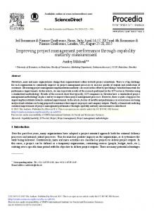
In order to cover the permanent faults of PCM, some extra storage (called ES) per line is usually used to cover such errors. The ES’s size is 12.5% of the line size. For a 512-bit line size, the ES is 64-bit (32 cells in 2-bit MLC). However, ES is not utilized until the line encounters first permanent faults. Therefore, this unutilized storage could be used for boosting the write/read operations, before the line faces permanent stuck-at faults. In order to analyze the utilization of ES section, first, we assume that the baseline system uses the well-known Error Correction Pointers (ECP)[47] scheme for hard error correction. ECP is considered as default correction scheme in many works (e.g. [26, 39]) because of its simplicity and low hardware overhead. In ECP, when a line faces stuck-at faults, its ES section is used to store some (6 in the original proposal) ECP entries. Each entry is responsible for correction of one failed cell; consequently, each entry contains a pointer to the position of faulty cell, and a cell that stores the correct value of the failed cell. Since each line has the correction power of 6 faulty cells, the method is called ECP6 . When a line encounters more than 6 faults, ECP entries are not sufficient to cover all, hence, operating system retires the page containing the faulty line in memory manager. In this paper, similar to other studies, we consider a page size of 4KB (i.e. 64 memory lines). Another issue that needs to be taken into account is different vulnerability of PCM cells to stuck-at faults, mainly because of process variation [23, 50]. The maximum number of tolerable writes for different PCM cells is expressed as normalized standard deviation (COV) around the mean value [39]. That is some cells are more prone to stuck-at faults and they may encounter hard errors at the beginning phases of PCM memory lifetime. Qureshi in [39] conducted an extensive study on the utilization of ECP6 entries and showed that many lines do not face stuck-at faults even at the final stages of PCM lifetime. Figure 8 shows the utilization of ECP6 entries during the lifetime of a PCM memory with COV=20% (it is based on Figure 2 in [39]). Figure 8 contains four curves. The FaultyLine curve shows the probability of a memory line to have at least one stuck-at cell at any point of PCM lifetime. In other words, it shows the percentage of memory lines that forced to use their ES section for error correction. LineFail curve shows the percentage of memory lines with more than 6 faults, where ECP6 is not able to recover all faulty cells and, therefore, the line cannot be used. PageFail curve shows the probability of pages to have at least one uncorrectable faults, meaning that they have at least one line with more than 6 faulty cells. Consequently, it shows the percentage of retired memory pages. We define the end of PCM lifetime when the memory capacity drops to half of its size. That is the endpoint is where the probability of PageFail is equal to 0.5 (as indicated in the figure). ACM Transactions on Architecture and Code Optimization, Vol. 0, No. 0, Article 0. Publication date: 0.
Improving MLC PCM Performance
0:13
FirstLineFail is the probability of PCM memory to face the first line failure. To be more specific, it indicates the point where PCM capacity starts to drop. The expected time to first page retirement is when FirstLineFail curve becomes 0.5. 1 0.9
FaultyLine
Probability
0.8
LineFail
FirstLineFail
PageFail
0.7 0.6
50%
0.5
C
0.4
27.2%
0.3
B
0.2 0.1
A
3.85%
75.5%
0 0
5
10
15
20
25
30
35
40
45
50
55
60
65
70
75
80
85.6% 85
90
95
100
Memory Lifetime(%)
Fig. 8. Failure probability vs time (as percentage of lifetime)
From Figure 8, we can conclude: • When memory reaches its half lifetime, only 3.85% of lines have faced stuck-at faults. This implies that more than 96% of lines have not used their ES section when memory passes half of its lifetime (point A in the figure). • When memory capacity starts to drop, still more than 72% of memory lines are healthy (point B). • When still 50% of lines have unused ES section, memory has passed 85.6% of its lifetime (point C). The expected rate of fault-free lines during the entire memory lifetime is therefore given by: ∫ 100 Averaдe_rate_o f _f ault − f ree_lines = (1 − FaultyLine(t))dt ≈ 83% (4) t =0
Equation 4 reveals that a significant amount of unutilized ES sections in the baseline system, and implies a good opportunity of using ES sections for performance improvement purposes. In the next section, we will show that it is possible to use this storage for performance improvement with a positive effect on memory wearout and energy consumption. 3.2
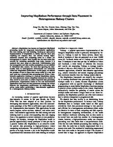
Relaxed Write/Read (RWR) Method
In our proposed method, Relaxed Write/Read (RWR), the extra storage is used for boosting the write/read performance. The ES is written in Tri-Level format. By using the coding technique proposed in [51], each pair of 2 Tri-Level cells represent 3 bits. Table 5 shows ternary to binary conversion. Since there are 32 ES cells per line, they could represent 48 bits in ternary format. These 48 bits are used to mitigate 48 HTW cells per line. This is done through a simple on-to-one mapping from an ES bit to a HTW cell. As Figure 9a indicates, we assume that the leftmost bit in ES corresponds to the leftmost HTW cell, one after the leftmost bit in ES corresponds to one after the leftmost HTW cell in line, and so on. Instead of writing these 48 HTW cells to their exact values, they are written to the intermediate state of Tri-Level format and their corresponding bits are stored in ES section to determine their exact value. Consequently, as Figure 9b shows, if the mapped bit in ES ACM Transactions on Architecture and Code Optimization, Vol. 0, No. 0, Article 0. Publication date: 0.
0:14
S. Rashidi et al.
section is "0", its corresponding HTW cell is "01", otherwise, the cell shows "10". In other words, the intermediate state of Tri-Level is used to mark 48 HTW cells and let their corresponding bits be stored in ES section to determine the exact state ("01" or "10"). In write operation, up to 48 HTW cells are detected and ES is filled according to the value of these 48 cells, before the write command is issued to memory array. In read operation, the corresponding ES is decoded from ternary to binary to represent the mapped bits; then, the memory controller finds up to 48 leftmost HTW cells of the line and correct their values by their corresponding bits in the ES. Finally, the final data line is delivered to the requester. RWR let up to 48 HTW cells be written in only 1 iteration, and therefore by decreasing the number of HTW cells, the average number of P&V iterations is decreased as well. Based on the number of HTW cells in each line two possible scenarios can be considered: • If the line has no more than 48 HTW cells, then all of them could be covered by ES bits. Consequently, the write operation is performed using 1 or 2 iterations (2 iterations if a cell with "11" value exists or if writing to intermediate state of Tri-Level requires another iteration). Since all line cells are in Tri-Level format, the Tri-Level read mechanism is used for subsequent reads to the line and therefore the read speed is improved. In Tri-Level read, if a data cell is in the first region, its value is "11", if it is in the third region, its value is "00". For the cells in intermediate region, their corresponding ES bit determines their exact value ("01" or "10"). We call such line to be fully-Tri-Level. • If the line has more than 48 HTW cells, the 48 leftmost HTW cells are written to intermediate state of Tri-Level format. Thus, the average number of P&V iterations is decreased. However, the subsequent read operations to the line is issued in MLC mode. In MLC read, the HTW cells that are written to intermediate state of Tri-Level mode are interpreted as "01" or "10", but their exact value is determined by their corresponding bits in ES part. The other HTW cells that could not be covered by ES are written exactly (in MLC mode) and hence are fully determined as in MLC read. Since the ES section is in Tri-Level format, in MLC read if a cell in ES is determined to be "01" or "10", then it is interpreted as the intermediate state of Tri-Level format. We call such line to be partially-Tri-Level. Using RWR, both read and write latency to the lines with no more than 48 HTW cells are improved significantly. Moreover, for the lines with more than 48 HTW cells the write latency is still improved. If a line encounters stuck-at failure, then its ES section is used for error correction purpose and RWR method cannot support the line. Data line(256 cells)
00 01 10 11 11 01
...
Data line(256 cells)
10 11 10 00 11 01
00 L1 L1 11 11 L1
0 Ternary to Binary Ternary to Binary
1
0
L1 11 L1 00 11 L1
1
1
...
L2 L2
ES(32 cells)
(a) Indicated mapping in RWR.
0
Ternary to Binary Ternary to Binary
L1 L2
... ES(32 cells)
...
(b) RWR correction.
Fig. 9. RWR mechanism. ACM Transactions on Architecture and Code Optimization, Vol. 0, No. 0, Article 0. Publication date: 0.
Improving MLC PCM Performance
0:15
As the memory lines could be in different states, the memory controller needs to track each line’s state. Therefore, 2 bits per line are needed to indicate whether the line is fully-Tri-Level, partiallyTri-Level or the ES is used for permanent failure correction. Therefore, the storage overhead of RWR method is about 0.4% (assuming 512-bit memory line size). For example, for a 16GB memory, 64MB storage is needed to track lines states. We let these state bits be stored in main memory in MLC mode, and a small cache, called line-state cache, in the memory controller is used to cache them. On every read/write request that is issued to memory controller, the memory controller adds the request to its corresponding read/write queue and then searches the line-state cache to determine the requested line’s state. If a miss occurs, the memory controller takes the state bits from main memory. If the state of next request to be serviced in any read/write queue is not determined, the memory controller stops servicing any requests from that queue until the state of the request is determined. The main memory also has a DRAM cache in order to hide the PCM read/write latency. Further, details on CPU&Memory organization is explained in Section 4. To make the RWR method compatible with DIMM structure, we reuse the Write Data Mask (DM) pins to indicate the cells that need to be written to intermediate state of Tri-Level mode. Originally, for write operation, each DM pin is used to mask its respective data byte (DQ) for any given cycle of the burst. In RWR method, the DM pin is used to indicate that all intermediate values of its respective DQ should be written to the intermediate state of Tri-Level. Figure 10 shows the usage of DM pin. If the DM pin is set to "1", then all of the intermediate values of its respective DQ are written to intermediate state of Tri-Level. Otherwise, the DQ is written in MLC mode. It is possible that in the last burst cycle, in one DQ, some HTW cells need to be written in Tri-Level form while other HTW cells must be written in MLC mode. In such cases, the Tri-Level write in the corresponding DQ is ignored and all HTW cells are written in MLC mode for the respective DQ. Therefore, in worst case, 45 HTW cells are covered rather than 48 cells3 . DM
DQ(8 bits)
DM
DQ(8 bits)
1
01 11 00 10
0
01 10 11 11 No change
Interpreted As
L1 11 00 L1
01 10 11 11
Fig. 10. Reusing DM pins for RWR method
3.3
RWR Encoder/Decoder
The RWR is a memory controller level technique. Therefore, CODEC circuits should be integrated with memory controller hardware. Such circuits should have low overheads in terms of power and area. In this section, we propose the Encoder/Decoder circuits for RWR method and evaluate their area, power and latency overheads. 3 This
condition occurs when DQ has four HTW values; three HTW values are covered by ES section and could be written in Tri-Level form, while other HTW values are not covered by ES. ACM Transactions on Architecture and Code Optimization, Vol. 0, No. 0, Article 0. Publication date: 0.
0:16
S. Rashidi et al.
3.3.1 Encoder. The encoding process happens when a new write request is placed to its corresponding write queue in order to be serviced by memory controller. While the write request is waiting for its turn in the write queue, the encoder circuit calculates the 48 correction bits to be stored in ES section in Tri-Level form. Writes are not on the critical path and have relatively high latency. In addition, reads have higher priority than writes for service. Therefore, the average queue latency of writes is sufficient to hide the encoder latency, even if the encoder is relatively slow, and hence, the encoder latency overhead does not have a considerable impact on overall IPC. Figure 11 shows the encoder circuit. The data is first loaded into a 256 × 2 shift register in one clock. Then, during each clock, the rightmost cell is checked, if it is a HTW cell, the ES shift register is enabled and the MSB of the rightmost cell is fed to the ES shift register. After each clock, the data shift register is shifted one cell to the right. If the ES shift register is enabled, it is also shifted one bit to the right. All of the data cells should be checked; therefore, after (1+256) clocks, the ES shift register has the correction bits corresponding to the 48 leftmost HTW cells. Consequently, the latency of encoder is 64.25 ns per line, assuming a 4GHz CPU clock. Further details about the area and energy overheads of the encoder appear in section 3.3.3.
1 1
0 1
1 1
0 0
1 0
0 0
0 1
1 1
Data In Enable
0
1
1
0
48-bit ES Shift Register
(256×2-bit) Data Shift Register XOR
Fig. 11. Encoder Circuit
3.3.2 Decoder. The decoding process begins when a new line is read from main memory by memory controller. Before the data is passed to the last level cache, it is first corrected by decoder circuit. Because the read requests are in the critical path, the decoder logic should be fast. Consequently, analyzing each data cell should be done in parallel with other cells. Figure 12 shows the decoder circuit. Lets say in each data line, celln is the data cell in position n where n=255 is the leftmost cell index and n=0 shows the rightmost cell. In order to perform parallel operations on data cells, each celln should know how many HTW cells are among its left-side cells; that is cell 255 ...celln+1 . Therefore, each HTW cell could determine whether it has a correction bit in ES section or not, and if yes, finds the location of its correction bit. In decoder circuit, first the bits of the cells are passed through XOR gates. The output of XOR gates –called HTW bits– determines whether the cell is HTW or not. Then, a set of carry-lookahead adders are used to sum the HTW bits and form partial sums. The partial sums are in Sn [i] format where n indicates the number of cells that are in the partial sum, and i is the index of that partial sum. For example S 2 [127] indicates that among cell 255 and cell 254 , how many HTW cells exist. Then, the partial sums are used to calculate the number HTW cells in the left-side of each cell, called offset. For example, for cell 255 , since it is the leftmost cell, the offset value is 0. For cell 252 , the offset is S 2 [127] + S 1 [253]. In the worst case, the maximum of 4 add/subtract operations among partial sums should be performed to calculate its offset (e.g. cell 224 ). When each cell determines its offset, its decoding operation can be performed independently. For each HTW cell whose offset is less than 48, a correction bit is considered in ES section. Cell’s ACM Transactions on Architecture and Code Optimization, Vol. 0, No. 0, Article 0. Publication date: 0.
Improving MLC PCM Performance
Data line(256 cells)
Data Position=0
Stage1
HTW Bits
1 1
XOR
0 1
XOR
0
0:17
Stage2
Stage8
S1[0]
8-bit Offset
Data
S256-s1[0]
1 1
Offset[5:0] If(data==HTW && offset