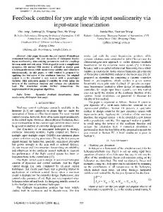
Including Many Power Electronics Converters: An. Analytical Investigation. A. Ales, M. E. Y. Boudaren, B. Karouche,. D. Moussaoui. Laboratoire SEM, Ecole ...
Input Impedance of Modern Embedded Networks Including Many Power Electronics Converters: An Analytical Investigation
Laboratoire SEM, Ecole Militaire Polytechnique BP 17 Bordj El-Bahri 16111 Algiers, Algeria Abstract—Power by wire concept is a novel trend in modern electrical systems. Hence, system networks have become more and more sophisticated, and their modeling is no longer an easy task. In this paper, we propose an analytical analysis of a global EMC of a modern electrical network. Explicitly, we develop an analytical model to evaluate differential mode impedance at different sites of a complex network. To this end, we use a Transmission Line “TL” theory applied in the case of bifilar cables. Bifilar cable parameters, such as the propagation constant and the characteristic impedance, are identified by measurement via the impedance analyzer Agilent 4294A. Such parameters are included into the analytical model for the computation process. The impedances, computed at different sites are compared to each other, and on the same time, to the impedance of Line Impedance Stabilization Network (LISN) in accordance with the CISPR 22 standard. To assess the model performance, we have carried out an experimental test bench. The measured impedances agree with those computed analytically. Keywords— EMC modeling; differential mode; common mode; EMC filter; LISN, EMI, conducted noise, impedance network.
I. INTRODUCTION Power converters are more and more integrated in electrical grids, particularly in embedded networks where managing input and output power forms are crucial [1]. For instance, Boeing ascertains that the electrical architecture on 787 is more power lossless than an equivalent pneumatic system [2], which illustrates how important is the “power by wire” concept. Let us also mention the car industry, where electrical networks are becoming too complex to be structured [3], mainly due to the increase of switching mode converters. Consequently, the major challenge in designing and optimizing modern electrical networks is to achieve an analysis of the global Electromagnetic compatibility (EMC) behavior in order to design optimal filters. However, such analysis subsumes the knowledge of the electrical network impedances, which are the converter impedances. Thus, the problem of converter impedance identification has been tackled in many studies: harmonic transient analysis [3], harmonic mitigation measurements [4], effective design EMI filters and their stability with power system [5], [6], [7], [8], [9] and [10], among other research frameworks.
A. Ales, Z. Gouichiche, J-L. Schanen, J. Roudet G2ELab, University of Grenoble Bat Ense3 BP46 F-38402 SMH Cedex, Grenoble, France
II. THE CONTEXT OF THE STUDY A modern electrical network includes a main power source which supplies all connected loads through a long main cable. Most of modern loads include more than one Power Electronics Converters (DC, AC…) [1], [2]. Since the power converters connected to the grid are excellent Electromagnetic Interference “EMI” generators, it is then necessary to study the global network behavior, including more than one converter, with respect to those ELM disturbances and then synthesize the adequate analytical models. Furthermore, many of engineers adopt EMC filters as a practical solution to reduce the EMI, especially after the design stage to avoid the ELM pollution comeback to the network. Hence, it is required to characterize both filter side’s impedances, which are the network and its inner converter as shown in Fig.1, in order to optimize the filter designs. Modeling and evaluating the network Common Mode (CM) and the Differential Mode (DM) impedances is a crucial step for filter optimization and its stability in the environment (no resonances). Moreover, the network impedance identification is likely to predict the "accurate" CM and DM disturbances without the use of the Line Impedance Stabilization Network “LISN”. Indeed, this device is not always representative of the actual impedance of real networks as mentioned in [8]. The aim of this paper is to highlight the accurate analytical computing process of DM impedances of a modern electrical network containing “more than one” converter in a frequency range, from very low frequencies up to few tens of MHz. Another purpose is to compute the impedance in any site of the network as in the nodal 0, nodal 1, etc. Experimental validation is conducted for each site. B e fo r e t h e f il te r
Z
Z0 No d a l 1 N et wo rk S ou r c e N o d al 0
N odal i
Z1
Fig. 1. The EMC filter environment
978-1-4799-7993-6/15/$31.00 ©2015 IEEE
A ft e r t h e fi lt e r
i
EM C F i lt er
CONVERT ER
A. Ales, M. E. Y. Boudaren, B. Karouche, D. Moussaoui
CV S
Zl
III. THE KNOWLEDGE BACKGROUND A. The DM impedance of the network The main purpose of this work is to develop an analytical model to compute the DM impedance of an electrical network including more than one converter. Therefore, one can compute the DM impedance ZDM through: Z DM =
VDM I DM
(1)
Fig. 3. The line model by the transmission line theory
The formula giving the input network impedance, containing a cable of length “l” (see Fig.4), according to the TL theory is expressed in (4) [12]. Zt may be DM or CM impedance and “j” is the imaginary complex number.
where IDM is the current circulating between the “L” and “N” conductors supporting the VDM voltage as illustrated in Fig.2. 'L' stands for Live (or "Line" or "Plus" for DC networks), 'N' for Neutral (or "Minus"), and 'G' is the reference potential (often earth or Ground). The problem to estimate the impedance at the input sides of the network (L, N and G see Fig.2) including the output impedance Zload, stems from the fact that the propagation phenomena inside the cable make it unworkable to apply the classical ratio V/I as in (1). Hence, one has to consider the cable length “l” and some parameters defined in the next section. B. The Transmission Line “TL” theory Since electrical networks contain relatively long cables, usually longer than an important signal wavelength circulating inside the conductors, it is a requirement to account the signal propagation phenomenon. To this end, one can use the transmission line (TL) theory, since the bifilar lines are Transverse Electro-Magnetic “TEM” lines, i.e. the electric field is transverse to the magnetic one [11]. Any TEM line is characterized by its primary and secondary parameters. The primary parameters are the line inductance “L”, the mutual capacitance “C”, the conductance “G” and the resistance “R” (see Fig.3). We assume that we have a lossless line where R=G=0. On the other hand, the secondary parameters are the attenuation parameter α, the phase parameter β, the propagation parameter γ and the cable characteristic impedance Zc [11]. Where:
Zc =
Li Ci
(2) (3)
Z t + j ⋅ Z c ⋅ tg ( β .l ) Z c + j ⋅ Z t ⋅ tg ( β .l )
(4)
IV. THE NETWORK IDENTIFICATION As mentioned previously, the network is composed of the source, the cable and the output impedances. The aim in this paper is to estimate the impedance inside the network at any point. Hence, one has to identify the different network components. A. The cable identification The cable used to constitute the network, in the experimental setup is a shielded twisted pair. The cable conductors are multi-bit with exterior diameter of 2.95 mm and inner diameter of 2.25 mm. The identification is performed using the impedance analyzer Agilent 4294A by means of four configurations as depicted in Fig. 5. The cable length is l= 2.46 m. Cases A and B are used to identify cable parameters (linear inductance and capacitance) for the DM network (Fig.5). Therefore in case A, “L” and “N” conductors form an open loop in order to measure the linear capacitance given in Table I. On the other hand, by shortening the other two sides of the same pair of conductors, the measurements give the linear inductance (Table I). The same thing is done for the remainder cases but the characterisation here concerns the shielding tress (“G” conductor) while the two rest conductors (L and N) are shortened at both terminal sides as illustrated in Fig.5 (cases “C” and “D”). Results are shown in the Table I. TABLE I.
• α is null because of a lossless line,
γ = α + jβ = jω p Li Ci
Z in = Z c
Capacitances Inductances
IDENTIFIED PARAMETERS OF THE NETWORK CABLES IN CM AND DM DM parameters
CM parameters
Cdm=199.3pF/m (Case A) Ldm= 1.38µH/m (Case B)
Ccm = 402.6pF/m (Case C) Lcm=152.39nH/m (Case D)
Li and Ci are respectively a per-unit inductance and capacitance of the cable.
Fig. 4. A simple network to compute the input impedance Zin along the cable of lenght “l”
Fig. 2. The synoptic diagram of the converter
Experimental identification
Now, the load impedance Zt and the cable being known, it is easy to perform the input impedance of the network Zin as presented in Fig.4 by using (4). V. THE NETWORK IMPEDANCES Let us assume now that we have a network architecture drawn in the Fig.7, including many branches (nodules), each one containing impedance Zi (which is a power converter). The challenge here is to compute and to measure the total network impedance at any point “Ni” considering all network phenomena, such as propagation’s, resonance’s, reflection’s and transmission parameters, etc.
Fig. 7. A Network architecture containing more than one branch
Fig. 5. An experimental setup for cable identification: case “A”, “B”, “C” and “D”
B. The laod impedance computation To compute the impedance Zin according to (4) as illustrated in Fig.4, it is necessary to know the Zt impedance in (4), which is the load impedance, and that may be a DM or CM converter impedance (for a modern network). In this paper, only a DM impedance of a more complex network is considered. Besides, we have demonstrated in previous works [12], [13] that the DM impedance ZMD of the DC converter is, in fact, mainly their input capacitor impedance ZCf, as expressed in (5) and presented in Fig.6. Z DM ≈ Z Cf
A. A simple network We have computed and measured in a previous work [12], the global DM impedance of a simple network (such as the structure shown in Fig.4) which does not contain branches, nor more than one converter. The result is illustrated in Fig.8.a. The result of Fig.8.b highlights the differences between simple network impedance (Fig.4) with complex network impedance (Fig.7), identified at the source point with the same primary and secondary parameters. The comparison shows that the architecture has an influence over a large frequency band. This result motivates us to perform a deeper study about complex network impedance at all points.
To summarize, one has to answer the following crucial questions: what will be the allure of that impedance, if we have many loads connected as represented in the Fig.7? And, is this impedance the same in all measurement points?
(5)
(a)
(b)
Fig. 8. The DM network impedance comparaison: (a) a theoritical result and the experimental measurement, (b) the impedance of a simple network with the impedance of a complex network
Fig. 6. The DM output impedance Zt of the network [12]
B. A more complex network In this part, we consider a more complex network containing “n” branches, to which are connected “n” converters. The length “lb” is considered the same for all branches: “lb = 25 cm”, as shown in Fig. 7. The space between two nodes Ni and Nj is named lij. The main line’s network
length is l = 2.46 m. We suppose that, except the source impedance Zs, no impedance exists at each point Ni. 1) The computing algorithm of the network impedance To perform the analytical formula of an “n” branches network impedance, for example at the “P” point, as in Fig.9, we have to follow the three following steps: • First, we have to bring back all branches impedance (Zi, Zj,...), as in Fig.9.a, to the main network line (as in Fig.9.b), using (4) considering the length “lb” of the branches and the cable characteristic impedance Zc, to get the new network line impedances ZNi, ZNj, etc. (Fig.9.b), • Then, beginning from the opposite point of “P” (“Nj” in Fig.9.b), we have to bring back successively, the impedances via (4) accounting for the space between the two points lij. For instance, we have to bring back ZNj to “Ni” point (Fig.9.b), • The impedance ZNj brought back to “Ni” will be associated to the “Ni” inner impedance ZNi (in parallel) to find the total impedance at that point Ztotal_Ni, • Finally, the total impedance at that point Ztotal_Ni will be brought back to the point “P” using (4) and accounting the lip length (as in Fig.9.b).
To sum up, the computation of the DM total network impedance ZNi at the nodal “Ni” results from the parallel association of all impedances at this nodal “Ni” coming from all branches (all nodes) using (5). 2) The analytical results of an "n" branch network In DM propagation, two conductors are used to feed the system (network). Since the two conductors form a bifilar line, it is possible to know the network input impedance using (4), by considering the cable identification in cases “A” and “B” of Table I.
Primary and secondary parameters, of the bifilar line here, are extracted from the measurements given in Table I. As a result, the characteristic impedance in this case (DM identification in Table I) is Zc=83.196Ω. Since we know that the DM impedances of the converter in the branch terminals is considered as its input capacitor [12], the Zi impedances in Fig.7 are considered as the impedance of that capacitor (Fig.6). Note that, the source impedance Zs is considered capacitive.
Fig. 10. The comparison between the LISN impedance, the cable characteristic impedance and the impedances computed in 10 different points of Fig.7
The spectrum DM impedances of a more complex network containing 18 branches (18 converters) connected to 18 nodes, identified at different points (nodes) are depicted in Fig.10. To start, all impedances below 100Hz are identical because of the absence of the propagation phenomenon at low frequencies (wavelengths are longer than conductors). Starting from this frequency, we outline some resonances associated to the propagation phenomenon and depending on the nodal position inside the network and the point of the measured. The network impedances are compared to the characteristic impedance (Zc=83.196Ω) of the cable (which is constant all along the cable). This comparison is relatively coherent starting from 30 MHz where the network impedances oscillate around Zc. Another confrontation is done with the DM impedance of a standardized LISN according to the CISPR 22 standard. The same conclusion may be extracted where network impedances swing around the LISN impedance starting from 30 MHz. This frequency may depend on the cable length and the number of branches (converters). Both comparisons are important in order to highlight the relationship between the network impedance, the LISN one and the characteristic one. So, even if after a certain frequency, the network’s impedances are relatively comparable to the LISN one, this result cannot be generalized to all frequencies (as demonstrated in Fig.10) due to the big difference between the two impedances over a large frequency range. This result, which is related to the prototype of the network considered in this work, can ascertain that the LISN impedance is not necessarily representative of the network and this can have repercussions on the filter optimization and design. VI. THE EXPERIMENTAL VALIDATION
Fig. 9. The computing process’s of the network impedance containing more than one branch
An experimental setup has been carried out as presented in Fig.11. The same network, used in the previous simulation to identify primary and secondary parameters, is employed here to measure the DM impedance in different sites. Also, the DM impedances are determined directly by the impedance analyzer (Agilent 4294A) as shown in Fig. 11 where the impedance analyzer terminals are connected to the “L” and “N” conductors of the network.
(d)
Fig. 11. Experimental setup to measure the DM impedance of the network by the impedance analyser Agilent 4294A
The capacitor impedances (Zi loads in more complex networks), included to evaluate theoretically the network impedances, using (4), are identified by the impedance analyzer to consider the real behavior (including the parasitical elements such as the serial inductance element “esl” and the serial resistance element “esr”). Fig.12 from “a” to “e”, shows the comparison between the impedance computed by theoretically and the experimental measurement at the different sites of the complex network (Fig.7). The comparison agrees for all case points.
(e)
Fig. 12. The DM impedance comparison of the network between the measured result and the theoretical result computed by the TL theory at different points: (a) the source nodal, (b) the nodal N1, (c) the nodal N2, (d) the nodal N3, (e) the nodal N4
VII. CONCLUSION In this paper, we have presented a mathematical model to compute the DM impedance of a modern electrical network, including more than one DC-DC converter, using transmission line theory of bifilar cables. An experimental validation is carried out to confirm the model’s coherence within a large frequency band in accordance with the CISPR 22 standard. (a)
(b)
(c)
As a first step, we have identified, by experimental measurements, all the network elements including the primary and the secondary parameters (propagation parameter, characteristic impedance, per unit capacitances and inductances of the cable) by means of Impedance Analyzer Agilent 4294A. The different impedances computed by the proposed model, taking into account experimental parameters, are compared to an impedance of a standard LISN to extract the relationship between them. The same comparison is achieved with the identified characteristic impedance. Then, the theoretical results are validated by an experimental test bench including the same network identified previously. It turned out that the measured impedances are comparables to those evaluated analytically for a large frequency band in accordance with the CISPR 22 standard. Finally, it is worth pointing out that the DM impedance of the tested network does not correspond exactly to the standard LISN (5-50Ω). In fact, for low frequencies, it is purely capacitive, whereas from 20MHz, it is not constant (50 Ω). Even if the tested network is relatively complex, one may not extrapolate such a conclusion to all networks from this single result. Still, it would be important, as a future direction, to compare the impedance of an actual network, using the proposed method, to the LISN standard, which is the standard governing all filter designs.
REFERENCES [1]
[2]
[3]
[4]
[5]
[6]
[7]
[8]
[9]
[10]
[11] [12]
[13]
[14]
M. Foissac, J.L. Schanen, C. Vollaire, “Black box EMC model for power electronics converter”, Energy Conversion Congress and Exposition, 2009. ECCE 2009. IEEE , pp. 3609 – 3615, 20-24 September 2009. I. Cotton, A. Nelms, "Higher Voltage Aircraft Power Systems", Aerospace and Electronic Systems Magazine, IEEE, vol. 23, pp. 25-32, 05 Mars 2008. J.M Poinsignon, P. Matossian, B. Mazari, F. Duval, "Automotive Equipments EMC Modelling for Electrical Network Disturbances Prediction", International Symposium on Electromagnetic Compatibility, 2003. EMC '03. 2003 IEEE , Vol. 1, pp. 415 - 417, 16-16 May 2003. M. Hartmann, H. Ertl, J.W. Kolar, “EMI Filter Design for a 1 MHz, 10 kW Three-Phase/Level PWM Rectifier”, Power Electronics IEEE Transactions on, vol. 26, NO. 4, pp. 1192 – 1204, April 2011. Touré, B.; Schanen, J.-L.; Gerbaud, L.; Meynard, T.; Roudet, J.; Ruelland, R.; , "EMC Modeling of Drives for Aircraft Applications: Modeling Process, EMI Filter Optimization, and Technological Choice," Power Electronics, IEEE Transactions on, vol.28, no.3, pp.1145-1156, March 2013 V. Tarateeraseth, Bo Hu, Kye Yak See, F.G. Canavero, “Accurate Extraction of Noise Source Impedance of an SMPS Under Operating Conditions”, IEEE Transactions on Power Electronics, vol. 25, No. 1, 11 août 2009. N. K. Poon, B.M.H. Pong, C.P. Liu, C.K. Tse, “Essential-coupling-path models for non contact EMI in switching power converters using lumped circuit elements”, Power Electronics, IEEE Transactions on, Vol.18, pp. 686 – 695, 26 March 2003. M. Reuter, S. Tenbohlen, W. Kohler, A. Ludwig, “Impedance analysis of automotive high voltage networks for EMC measurements”, EMC Europe 2011 York, 26-30 September 2011. Y. Panov, M. Jovanovic, “Practical Issues of Input/Output Impedance Measurements in Switching Power Supplies and Application of Measured Data to Stability Analysis,” in Applied Power Electronics Conference and Exposition, 2005. APEC 2005. Twentieth Annual IEEE, vol. 2, pp. 339 – 1345, 6-10 March 2005. Jian Sun, K.J. Karimi, “Small-Signal Input Impedance Modeling of Line-Frequency Rectifiers”, IEEE Transactions on Aerospace and Electronic Systems, Vol. 44 , pp. 1489 – 1497, October 2008. P.F. Combes, “Microwaves” xth ed. Belgium, January 1996. A. Ales, JL. Schanen, D.Moussaoui, J. Roudet, "Impedances Identification of DC/DC Converters for Network EMC Analysis", IEEE Transactions on Power Electronics, Vol.PP , Issue: 99, page 1, 11 February 2014. A. Ales, JL. Schanen, D.Moussaoui1, J. Roudet, "Experimental validation of a novel analytical approach about a DC-DC converter input impedance", EPE2013 ECCE Europe, Lille, France, sept 2013. A. Ales, G. Frantz, JL. Schanen, D.Moussaoui, J. Roudet, “Common Mode Impedance of Modern Embedded Networks with Power Electronics Converters", EMC Europe 2013, Brugge, Belgium, Sept 2013.