... Balasa, Eric Beeckmans, Filip Thoen, Filip Louagie, Koen Van Nieuwenhove, Karl ... 4] H. De Man et al., \Architecture-driven synthesis techniques for mapping ...
Integration of medium-throughput signal processing algorithms on exible instruction-set architectures� Gert Goossens Koen Schoofs
Dirk Lanneer Marc Pauwels Francis Depuydt Augusli Ki i Marco Corneroy Paolo Petroni Francky Catthoor Hugo De Manz IMEC, Kapeldreef 75, B-3001 Leuven, Belgium
Abstract
Integrated circuits in telecommunications and consumer electronics are rapidly evolving towards single chip solutions. New IC architectures are emerging, which combine instruction-set processor cores with customised hardware. This paper describes a highlevel synthesis system for integration of real-time signal processing systems on such processor cores. The compiler supports a exible architectural model. It can handle certain types of incompletely speci ed architectures, and o�ers capabilities for retargetable compilation and architectural exploration. Results for a realistic application from the domain of audio processing indicate the feasibility and power of the presented approach.
1 Introduction The electronic systems industry of the nineties is confronted with the challenge of integrating complex multi-functional systems in silicon. High-volume markets like end-user telecommunications and consumer electronics require cost e�cient solutions in the form of applicationspeci c IC architectures [1]. In the past decade, systems were mostly built by designing separate application-speci c IC's for di�erent functions, which were then put together on a board. The architectural styles used in these IC's can be divided into two major classes [2] : � Solutions based on eld or mask programmable instruction-set processors ; � Solutions based on custom datapath architectures . Today, there is a clear trend towards the integration of complete systems on a single chip . This results in a signi cant reduction of the IC and board cost, of the physical volume of the product, and of its power consumption. These factors are of vital importance for portable, low cost systems. System-level integration implies that multiple system functions, for which di�erent architectural styles are preferred, are put together on a chip. � y z
To appear in Journal of VLSI Signal Processing (special issue on synthesis for real-time DSP), 1993. University of Genova, Italy. Professor at Katholieke Universiteit Leuven, Belgium.
1 To be published in : Journal of VLSI Signal Processing, 1994. Copyright Kluwer Academic Publishers 1994.
(hardware)
(software)
memory
Accelerator datapath
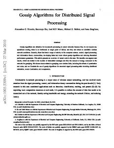
RAM DSP Coreof heterogeneous In [3], the concept IC architectures for real-time signal processing systems µ-Sequencer has been described. The idea is to combine architectural modules of the following types on Accelerator a single chip : the core of a programmable instruction-set processor, one or more customised datapath control datapaths,Master memories and logic (see Figure 1). The processor core is used to implement system functions with low to mediumRAM throughput (sample frequency). By virtue of its programmaGlue bility, logic late speci cation Interface changes or customer-speci c features can be accommodated rather easily. Customised datapaths, on the other hand, are used to implement high-throughput parts of the algorithm. They can be viewed as accelerators for time-critical functions.
Figure 1: Outline of heterogeneous IC architecture for real-time signal processing systems. In this context, architectural synthesis for complex signal processing systems amounts to a hardware/software co-design problem. The hardware component of the design problem consists of synthesising the accelerator datapaths. The software component consists of the generation of embedded microcode for the instruction-set processor core. This paper describes the Cathedral 2nd high-level synthesis system1. Cathedral 2nd is a compiler for exible microcoded instruction-set architectures , in the domain of real-time signal processing systems in the low to medium throughput range, i.e. with sample frequencies up to a few hundred kHz. Cathedral 2nd generates highly optimised microcode, starting from an algorithmic speci cation in the form of a signal- ow graph and a fully or incompletely speci ed description of a target architecture . The compiler has the following attractive features : � It o�ers a large exibility in the de nition of the target architecture. The user can build a wide variety of processor datapaths , by selecting microprogrammable building blocks from a library and connecting them in an appropriate way. As such, Cathedral 2nd provides a rst step in the direction of a retargetable microcode generator , i.e. a system that can generate code for any microcoded architecture speci ed by the designer. In the current version of the compiler, retargetability is provided with respect to the datapath component of the architecture. Retargetability with respect to the controller component is still restricted : currently only a horizontal VLIW controller model is supported, which implements conditions through multi-way branching. This model The methodology implemented in the methodology described in [4][5]. 1
Cathedral 2nd
2 To be published in : Journal of VLSI Signal Processing, 1994. Copyright Kluwer Academic Publishers 1994.
compiler is a follow up of the
Cathedral II
is di�erent from the controller architectures used in several existing commercial DSP cores. The controller implementation is currently based on microcode stored in ROM, and includes application-speci c logic circuitry. As a result, eld programmability is not supported today. Extensions are however under way to alleviate these restrictions. This will result in a powerful microcode compilation environment for heterogeneous IC architectures. � It can handle architectures in which the register structure and interconnection network are not or incompletely speci ed. These elements will then be determined and optimised by the compiler during the synthesis process. For example, the compiler can determine the required size of register les, and the required interconnections between di�erent datapaths or between datapaths and memories. This is a powerful feature : in practice, a designer can rather well judge about the required arithmetic building blocks for a certain application, but not about the register and interconnect requirements. As such, Cathedral 2nd provides capabilities for interactive architectural exploration . For a given application or even for a set of applications, the designer can design an applicationspeci c programmable processor by specifying the basic arithmetic blocks and leaving the architectural re nement and the code generation to the compiler. The synthesis process is fast enough to allow several design iterations in a short period of time. This paper is organised as follows. Section 2 contains a literature survey on high-level synthesis and on code generation work. In Section 3, the architecture model supported by the Cathedral 2nd compiler is introduced. Section 4 describes the data models used in the design process, and the way they are supported by the compiler. Section 5 outlines the overall synthesis trajectory. The di�erent steps are described in more detail in Sections 6 and 7. Conclusions are drawn in Section 8.
2 Literature survey Architectural or \high-level" synthesis is a very active eld of research [6]. Today a lot of e�ort is spent on well de ned but isolated problems , like scheduling and binding. As a result, the theoretical basis of high-level synthesis is clearly growing. A major challenge is to design a compiler that covers the complete trajectory from behavioural speci cation language to layout, and to demonstrate its use on applications of industrial size. A few attempts in this direction have recently triggered industrial interest [7][4][8][9][10]. Most of this work is oriented towards synthesising a customised datapath architecture that is tuned to one speci c signal processing function. This approach is well suited for high-throughput systems (e.g. video or image processing), where the architectural topology needs to be highly customised to meet the speed constraints. These techniques can be used to synthesise accelerator datapaths in a heterogeneous architecture as show in Figure 1. For low to medium throughput functions (e.g. audio, speech processing, or end-user telecom), extreme customisation of datapaths is not required. In this case, a programmable processor architecture can be de ned for a set of applications. The main challenge now is to map large ow graphs in an e�cient way on a partially or fully speci ed instruction-set architecture [3][11]. In the high-level synthesis community, only few authors have addressed this problem. Mimola [12] contains a retargetable code generator for a class of non-DSP architectures. The 3 To be published in : Journal of VLSI Signal Processing, 1994. Copyright Kluwer Academic Publishers 1994.
address
data
STATUS LOGIC
Progr'ble adder
Register file
Progr'ble shifter
BRANCH LOGIC
Latch
µC-to-Silicon [13] and Cbc [14] compilers can generate microcode for programmable DSP +1
architectures. The central idea behind bothCompacompilers is to investigate CODE di�erent data distriPROG. rator ROM CNT. bution strategies during the scheduling task, in a process called data routing. C-to-Silicon LOCALmodel CONTROLLER INSTR.REG is based on a dedicated architectural which restricts the retargetability of the compiler. Cbc supports a microcoded machine model with a special-purpose machine description MICROCODED CONTROLLER language [15]. None of these systems allows to enter incompletely speci ed architectures. Retargetable code generation has been studied in compiler theory and in the context of microprogramming, in the early eightees. An overview of techniques can be found in Ganapathi's paper [16]. In general, these techniques do not consider real-time applications, and they are tuned towards conventional Von Neumann architectures which di�er signi cantly from modern parallel RISC or VLIW processors. Interesting results in the domain of microprogramming have been reported by Vegdahl and Mueller [17][18]. Although machine-independent code generation is intended, a labour-intensive preprocessing step is required before switching the target. This is necessary to allow the user to optimise the implementation of data transfers during code generation. These approaches are especially useful for infrequent retargeting, which excludes their use in a design exploration environment. An alternative approach to retargetable code generation has been implemented in the Mpg compiler [19]. This approach is tuned to processors with a specialised instruction sequencer model. Today, instruction-set architectures are appropriate for low to medium throughput signal processing functions. However, technological evolution results in a continuous performance improvement of such architectures. Of-the-shelf programmable instruction set processors are already being introduced in the domain of video and image processing, and rst compilers are being developed [20]. A growing importance of retargetable code generation techniques can therefore be predicted, for the next ve years.
3
Cathedral 2nd's
architecture model
Cathedral 2nd supports a exible microcoded ASIC architecture model, controlled by a
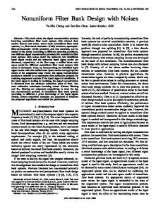
horizontal VLIW controller. In this section, the architecture model will be introduced. The architecture consists of three parts : the datapath, the memory structure, and the controller. Figure 2 shows a typical architecture, as obtained after completion of the synthesis process.
Figure 2: A typical Cathedral 2nd ASIC architecture, containing a centralised RAM, customised EXU's, and a microcoded controller.
4 To be published in : Journal of VLSI Signal Processing, 1994. Copyright Kluwer Academic Publishers 1994.
3.1 Datapath model
A Cathedral 2nd datapath consists of a number of microprogrammable entities called execution units or EXU's [21]. EXU's can be composed in a exible way, by selecting primitive hardware building blocks from a library, and connecting them using local interconnections . The building block library currently contains some 30 parametrised elements, including adders, shifters, comparators, multiplexers, registers, decoders, shift registers, etc. An EXU contains registers or register les located at each data input. This register structure permits \foreground storage" of signals, i.e. the execution of an operation and the access of its operands can be performed in the same machine cycle. EXU's can optionally be provided with a local controller, to decode instructions sent by the processor controller (see Section 3.3), or to speed up time critical decision making. The set of EXU's that can be built is very large. The compiler can support any combination of building blocks connected according to the EXU model. Moreover, extensions of the model are under way, e.g. to support EXU's without local registers at their data inputs. Data communication between EXU's occurs over a bus network. The model supports both direct connections and shared busses. As mentioned in Section 1, Cathedral 2nd can handle incompletely speci ed datapaths. Optionally, the following elements of the architecture can be left unspeci ed : the size (number of words) of the register les, and the bus network between the di�erent EXU's or between EXU's and memories (see Section 3.2). These elements can be synthesised by the compiler, which will try to minimise the associated silicon area subject to a constraint on the overall execution time.
3.2 Memory model
Signal processing applications typically contain one or multi-dimensional array data types. To store these arrays, memory is provided. In a Cathedral 2nd architecture, the memory structure typically consists of one or two central RAM's, possibly with additional pointeraddressed memories for realising delay lines [2]. Communication between memories and EXU's occurs over the bus network. In contrast to registers (see Section 3.1), the memory structure can only be used for \background storage", i.e. each access to memory requires a separate machine cycle.
3.3 Controller model
The datapath and memory architecture is controlled by a microcoded controller. Currently, a horizontal VLIW controller model is supported [22], as shown in Figure 2 (right). Such a model is well suited for parallel architectures. Figure 3 shows the instruction word model. The di�erent elds in the instruction word are orthogonal, i.e. they can be set independently. When an EXU does not contain a local controller, separate orthogonal elds can be provided for each of the composing building blocks. The controller implements conditions through multi-way branching. For that purpose, dedicated logic is added for status handling and branch address generation. The function of these logic blocks is controlled via separate elds in the instruction word, in parallel with and orthogonal to the datapath and memory instruction elds. Due to the presence of status and 5 To be published in : Journal of VLSI Signal Processing, 1994. Copyright Kluwer Academic Publishers 1994.
reg.file reg.file 1 2
EXU core
reg.file reg.file 1 2
EXU core
Figure 3: Generic instruction word model. branch logic, the controller is currently not eld programmable. The microcode is stored in ROM. Work is under way to circumvent this restriction. The content of the microcode ROM and of both logic blocks is determined by the compiler during the synthesis process.
4 Design representation and the data model backbone The Cathedral 2nd compiler is built on top of a software backbone, implementing an object-oriented data model [23]. This backbone acts both as a central data structure and as a uni ed design representation at all design levels in the synthesis trajectory. A rule base , containing methods for design transformation , forms an integral part of the backbone. Although tuned to real-time signal processing problems, the backbone is highly independent from the architectural styles and the application domains supported by the compilers which are integrated on top of it. Currently, the backbone is in use by several high-level synthesis systems : Cathedral 2nd, Cathedral 3 [24] and Cbc [14]. Throughout the synthesis process, any design can be consistently represented using two linked information models : a signal- ow graph model to represent the algorithm under synthesis, and a netlist model to represent the architecture. Hence, the backbone provides two linked information kernels (see Figure 4) : the DSFG kernel (decorated signal- ow graph) and the ANL kernel (architecture netlist). The DSFG{ANL links which indicate operation-tohardware bindings, as well as the scheduling information, are introduced during the synthesis process and are represented by means of attributes to DSFG nodes. The input speci cation of Cathedral 2nd consists of an algorithmic description in the data- ow language Silage [25], and an architectural description (of a partially de ned architecture) in the netlist language Hilarics [26]. These textual inputs can be translated into the DSFG and ANL models respectively. The output of the compiler is a detailed and complete netlist description, which can be sent to a layout generation environment based on regular modules or on standard cells, and a controller description which can be sent to a controller and logic synthesis environment [27]. These outputs are available in the ANL and DSFG formats respectively. In addition to the DSFG and ANL kernels, a LIB kernel (library) is provided in which a designer can describe the behavioural and structural primitives available to the compiler, i.e. all high-level operations (functions) and all building blocks with their local instructions. Moreover, the LIB kernel contains transformation rules describing alternative implementation schemes of these operations onto hardware (see Section 6.1 for details). For all three information kernels, both a binary and a textual representation are de ned 6 To be published in : Journal of VLSI Signal Processing, 1994. Copyright Kluwer Academic Publishers 1994.
DATA ROUTING
MEMORY MANAGEMENT FLOWGRAPH REFINEMENT
DSFG
OPERATION CHAINING
ANL
INTERCONNECT DEFINITION
SCHEDULING
LIB CONTROLLER MAPPING
EXU ASSIGNMENT
Controller spec
Final netlist TO SILICON IMPLEMENTATION
Figure 4: Operation principle of Cathedral 2nd's data model backbone. and maintained during synthesis. The textual DSFG and ANL representations can be used by designers as an archival data base . In this way it is possible to store intermediate results at any level throughout the synthesis trajectory, or to resume a synthesis session based on previous intermediate results. An important aspect of use is the adaptability of the LIB data kernel . Although one standard LIB description has been developed for Cathedral 2nd, the user can easily extend the LIB with new operations, operators and transformation methods (rules) when desired. This is accomplished through a user-friendly textual LIB format. Fore more details about the backbone concept, the reader is referred to [28].
5 Overview of the compilation process
5.1 Design example : dynamic-range compression system
Throughout this paper, the concepts and techniques will be illustrated on a practical example. The application selected is a dynamic-range compression algorithm for digital audio, published in [29]. The purpose of this algorithm is to adapt the dynamic range of an audio signal to the listening situation. The acceptable dynamic range is determined by the background noise level (for low-level passages) and by the maximal acceptable sound level (for high-level passages). The main signal ow in the algorithm is indicated by the block diagram of Figure 5. The stereo signals are sent through a DC o�set lter and a delay line, while the gain factor by which they must be multiplied is calculated in parallel in a feedforward control path (bottom of gure). With a clock frequency of 15 MHz, 339 instruction cycles are available to compute the entire algorithm.
5.2 Starting point
Figure 6 shows an example of an initial ANL and DSFG description, as provided by the designer at the start of the compilation process. The ANL description shown is the target architecture of the dynamic-range compression chip. The DSFG description shown corresponds to the left channel of the DC o�set lter (see Figure 5). 7 To be published in : Journal of VLSI Signal Processing, 1994. Copyright Kluwer Academic Publishers 1994.
sign
24
/
ALU 24
/
SH 1
CONSTANT DECODER
24
24
/
mean sign
/
24
ALU 24
24
/
SH 1
ANL
+/s
in
ampli
/ 24 1 24 / MPY 34 delay / / / 10 24x10 / 1 / / comp. OUTPAD 1 level loop exp. 24 / 1 / / CONS- 24 TANT / ROM 8 8 24 / / / RAM 24
offset SIGN
/
SIGN
inright
1 INPAD
CONSTANT DECODER
24
= add with saturate
b
16
24
outright
cast
24
*
24
48
+
cast
24
24
+/s out
24
DSFG
Figure 5: Top level signal ow graph of the dynamic-range compression system. Functions \mean", \compress/expand", \delay", and \ampli" contain programmable modes.
Figure 6: Example of ANL and DSFG input, provided by the designer.
� Initial ANL : The designer de nes the necessary memory elements, with their size and
number of ports. Furthermore, the designer de nes a set of customised EXU's. Each EXU is described as an interconnection of instanciated building blocks selected from the LIB. The size of the register les at the EXU's inputs, as well as the content of the router boxes (marked with an \X" in the gure) are unknown. Router boxes serve to align the bits of the signals on the available hardware (see Section 6.5). Furthermore, the interconnection network between EXU's and memories is unknown as well. � Initial DSFG : The starting point is a high-level DSFG description containing \algorithmic" operations, which often cannot be directly mapped onto the building blocks described in the ANL kernel. Examples of algorithmic operations are a division, arithmetic operations on complex or oating point numbers, etc. For every algorithmic operation, several alternative implementation schemes may be stored in the LIB kernel, each with di�erent area/time tradeo�s .
5.3 Design script
Figure 7 outlines the design script for mapping an algorithm onto a Cathedral 2nd architecture. The design trajectory contains three major phases ; the second and third phase are supported by the Cathedral 2nd compiler. 1. Memory management : In this phase, all array signals are bound to memory locations and to access ports in the available memory structure. As shown in [30], the required 8 To be published in : Journal of VLSI Signal Processing, 1994. Copyright Kluwer Academic Publishers 1994.
MEMORY MANAGEMENT
DATAPATH MAPPING FLOWGRAPH REFINEMENT OPERATION CHAINING EXU ASSIGNMENT
SCHEDULING
DATA ROUTING
SCHEDULING
INTERCONNECT DEFINITION
SCHEDULING
CONTROLLER MAPPING
Global netlist
TO SILICON IMPLEMENTATION
Figure 7: Design script. Shaded parts are supported by the Cathedral 2nd compiler. memory size and bandwidth can be drastically reduced by applying automated control
ow transformations on the initial signal- ow graph. Such transformations allow to fold individual array elements onto the same memory location. In complex signal processing systems, memory often constitutes a critical resource. Therefore, memory optimising transformations should be applied in the very rst design phase, until the memory requirements comply with the available memory space and bandwidth. After memory management, all memory accesses should be indicated in the DSFG description by means of \memory read" or \memory write" operations, assigned to memory ports in the ANL description. For every access to memory, an address must be provided. The corresponding address calculations have to be added to the DSFG description. The control ow transformations are re ected in the DSFG's loop structure. 2. Datapath mapping : In this phase, the DSFG description is rst transformed whereby each high-level algorithmic operation is replaced by a set of low-level \building block operations". Each building block operation can be mapped directly onto at least one building block instance available in the datapath. This transformation process is termed
owgraph re nement . Next, the re ned owgraph (described in the DSFG kernel) is mapped onto a given EXU con guration (described in the ANL kernel). In this step, various binding decisions are made between DSFG elements, ANL elements, and the time axis (see below). In case the architecture is incompletely speci ed, its remaining parameters (interconnection network, register le sizes, routing boxes) are determined. 9 To be published in : Journal of VLSI Signal Processing, 1994. Copyright Kluwer Academic Publishers 1994.
Datapath mapping is a complex process which strongly interacts with scheduling . A global optimisation approach is infeasible for practical applications. Therefore, in the Cathedral 2nd compiler, the datapath mapping process is divided into several subtasks as shown in Figure 7. In each subtask, one speci c type of binding is determined : � Operation chaining and EXU assignment determine the binding of operations to building blocks and EXU's; � Data routing determines the binding of scalar signals to registers and to routing paths; � Interconnect de nition synthesises the bus network and determines the bit-wise alignment of signals on available wires. Within each subtask, an intermediate schedule is constructed. Each of these schedules (except for the last one) is an approximation , because it cannot take into account resource con icts related to hardware bindings to be determined in a later subtask. However, the obtained scheduling views are su�ciently accurate to steer the search process in each subtask, and in practice the di�erences between the various scheduling passes are small. The datapath mapping tools are able to handle any type of EXU's de ned according to the model described in Section 3. 3. Controller mapping : In the last phase, the scheduled DSFG description is mapped onto the microcoded controller structure . The content of the microcode ROM is determined as well as a logic description for the status and branch logic, needed to implement data-dependent decision making. The datapath and controller mapping phases, which are covered by the Cathedral 2nd compiler, are described in more detail in Sections 6 and 7.
6 Datapath mapping 6.1 Flowgraph re nement
Flowgraph re nement is a transformation process on the DSFG description during which every algorithmic operation is replaced by a set of building block operations, each of which can be mapped directly onto at least one building block instance available in the datapath. This is a non-trivial process, since various design tradeo�s can be made. In the LIB kernel of the data model backbone, a variety of implementation schemes is described, for each algorithmic operation . The implementation schemes are organised in a re nement tree . Figure 8 shows a part of the re nement tree, describing the algorithmic operation \multiply" (\*"). In this case, tradeo�s can be made between single and multiple precision arithmetic , parallel implementation on a Booth multiplier, serial implementation on an ALU, etc. With an implementation scheme, a parametrised sub- owgraph may be stored termed its \DSFG-view", that indicates how the high-level operation can be implemented using low-level operations from the re nement tree. Examples of parameters are signal types of operands, the multiplicity in case of multiple precision arithmetic (double, triple, : : : precision), etc.
10 To be published in : Journal of VLSI Signal Processing, 1994. Copyright Kluwer Academic Publishers 1994.
... sgle-prec on MPY
on ALU
• operator()
• DSFG-view();
mple-prec with cst on ADD • DSFG-view();
with
... with
sgle-prec acc. dble-prec acc. • DSFG-view();
• DSFG-view();
Figure 8: Part of Cathedral 2nd's re nement tree, showing various implementation schemes of the multiply operation. The owgraph re nement process is handled by the tool DsfgExp. This tool selects a speci c implementation scheme for the algorithmic operations, determines the necessary parameter values, and carries out an expansion of the owgraph based on the selected parameter values and on the DSFG-views in the re nement tree. Expansion implies a recursive call to other nodes in the re nement tree, until all operations in the DSFG can be mapped onto building block operators. When alternative implementation schemes are available for a given operation, DsfgExp picks the rst one stored in the LIB that can be realised on the given datapath. This choice can however be overruled by the designer. In the o�set lter example (see Figure 6), a multiplication occurs of two 24-bit signals, yielding a 48-bit product. These large wordlengths are typical in audio applications. On the other hand, the datapath contains a 24�10-bit multiplier building block and two 24-bit ALU's. In this case, the designer selects a multiplication scheme with one triple-precision operand and with double-precision accumulation , from the LIB [31]. Figure 9 shows possible re nements of the multiplication, including expansion, for two sets of parameters. The re ned graph of Figure 9 (b) can be implemented on our target architecture. The availability of a LIB kernel containing many implementation alternatives, allows to make e�ective tradeo�s in the architectural search space . For example, the use of multiple precision arithmetic leads to a signi cant reduction of the necessary datapath area, at the expense of execution time (required number of clock cycles) and controller area. In real-time signal processing applications, like envisioned by Cathedral 2nd, the execution time is normally speci ed as a result of the sample rate speci cation. Therefore, the intention is to nd a solution with minimum controller area, that satis es both the resource and throughput constraints.
6.2 Operation chaining
Complex EXU's typically contain multiple building blocks, connected in a single combinational path. An example is the ALU-SIGN-SHIFT combination in Figure 6. The power of these EXU's is in the fact that they can execute patterns consisting of multiple operations , which occur in the re ned DSFG, in a single clock cycle . The purpose of the operation chaining tool Choice is to detect patterns in the DSFG description which can be mapped on the available EXU's, and to determine all legal bindings 11 To be published in : Journal of VLSI Signal Processing, 1994. Copyright Kluwer Academic Publishers 1994.
2
2 16
16
8
split
24 bits
split
24
split
split
split
cat cat
= carry flow
p (a)
split
sign
24 bits
p
48 bits
48 bits
sign
cast cast cast cast
12 bits
8
12 bits
8 bits
sign split
split
32 bits
b 24
split
p
(b)
48 bits
bits
24 bits
a
split
(c)
Figure 9: Two re nements of a 24�24-bit multiplication, using multiple precision arithmetic. of these patterns to the EXU's. For one pattern, several bindings may be possible. A binding is legal if the di�erent building blocks in an EXU can be set in the appropriate control mode to execute the pattern. For example, to execute a simple addition on the ALU-SIGN-SHIFT EXU, ALU has to be set in \add" mode and SHIFT has to be set in a transparent \pass" mode. After chaining, all selected patterns (including single-operation patterns) are replaced by single nodes, called EXU operations . The chaining tool uses a graph-based clustering technique [32] that tries to come up with a minimal number of EXU operations , as this results in a low machine cycle count. The technique is di�erent from traditional instruction selection techniques used in software compilers [33, pp. 572{580], in two respects. First of all, no prede ned list of patterns is used, but the legal patterns are automatically derived from the given EXU structure. Secondly, the selected patterns can be general graph structures rather than traditional expression trees. Patterns may be found that cross the boundaries of loops, conditional branches, or common subexpressions. During the chaining process, Choice produces statistical information that can be used by the designer to tune the datapath composition. For example, Choice prints a list of frequently occurring DSFG patterns for which no legal bindings could be found due to limitations in the EXU composition. In the o�set lter example (Figure 6), Choice successfully identi ed a number of \addsign" patterns in the DSFG, matching on the ALU-SIGN-SHIFT EXU.
6.3 EXU assignment
At this level of the design script, the DSFG consists of EXU operations, each with a list of legal bindings to EXU instances. The nal binding of these operations to EXU instances is performed by the EXU assignment tool ExuSel. A heuristic assignment technique is used that minimises the number of data transfers between di�erent EXU instances [34]. This results in a reduced bandwidth requirement for communication between EXU's, so that a low-cost (possibly shared) bus network can be synthesised later on (see Section 6.5). 12 To be published in : Journal of VLSI Signal Processing, 1994. Copyright Kluwer Academic Publishers 1994.
pass
tn-1
t1
t1
t1
t1
tn t1 tn store in register spill to memory
t2
broadcasting
serial routing
direct
converse
To obtain good results, the EXU assignment process should be steered with scheduling multi-read delay line information (cf. Figure 7).from Formemory this reason, an initial schedule is computed in a preprocessing stept before callingt thet ExuSelt tool. The only type of resource constraint that is accounted t t t t for in this scheduling pass is the available number of EXU instances; therefore the obtained t t t schedule The actual scheduling t technique will be t t of the nal t one. t t t will be an approximation circulating discussed 6.6. multi-fetch serial routing FIFO single fetch recomputein Section buffer In the o�set lter example, the EXU RAM assignment technique allows to nd an e�cient assignment of operations to the di�erent instances of the ALU-SIGN-SHIFT unit.
multi-consumption signal
pass
t1
t2
1
2
1
2
1
1
tn store
n-1
n
n
n-1
n
pass
1
2
1
1
1
1
1
6.4 Data routing
The purpose of data routing is to select a routing path for every scalar signal in the DSFG. This path will be used to transport the signal from the output port of the EXU where it is produced to the input ports of the EXU's where it is consumed. A routing path consists of interconnections, registers and/or memories, and in some cases also of EXU's that execute a transparent \pass" instruction. The data routing process includes the binding of signals to registers, commonly known as register allocation . After data routing, every operation in the DSFG corresponds to a data transfer between registers or memories; these operations are called register transfer (RT) operations . For a given signal, a direct connection between the producing and consuming EXU (via an intermediate register) is not always desired, as this may result in excessive register and interconnect cost. E�ective area/time tradeo�s can be made. In the case of a prede ned register and/or interconnect structure, certain direct connections may even not be allowed. The search space of the data routing task is large, as is illustrated by the following nonexhaustive list of tradeo�s (Figure 10) :
Figure 10: Typical tradeo�s in data routing. Labels t denote time steps at which data transfers occur. i
� Signals with multiple destinations can be transferred from the EXU output port where they are produced to each of their destinations, either via parallel broadcasting , or via serial routing (through EXU's that can execute a \pass" instruction); 13 To be published in : Journal of VLSI Signal Processing, 1994. Copyright Kluwer Academic Publishers 1994.
� Signals with long lifetimes can be kept in a register ( le), or temporarily spilled to memory to free the register. Spilling is indispensable in architectures with limited registers or with register les of small sizes [35].
� In the case of a commutative operation, the operands can optionally be switched . � Signals which are to be consumed twice in an EXU, can be produced once and then stored
until the last consumption, or can be recomputed on every consumption . A special case occurs when the source of the signal is a memory : the above alternatives then amount to single fetch from memory followed by foreground storage in a register or register le, and to multiple fetch from memory respectively. � Signal delay lines (as for example in digital lters) can be stored in RAM, with a circulating address scheme , or stored in a FIFO queue , or serially routed between registers . The data routing tool Amnesia tries to nd a solution that minimises the area cost within the execution time constraint. To that extent, a branch-and-bound search strategy has been developed, which makes use of reliable estimators for the actual hardware cost (i.e. the impact of a data routing decision on register and interconnect cost) and the actual execution time (i.e. the impact on the schedule) [36][28]. The execution time is estimated by building a probabilistic scheduling view, which is updated during the data routing process (cf. scheduling interaction in Figure 7). In the example of the o�set lter, the data routing technique allows to nd an e�cient implementation of the delay lines (see feedback arcs in Figure 6 (b)), by means of serial routing.
6.5 Interconnect de nition
For architectures with an incompletely speci ed bus network, the actual interconnection structure can be de ned after data routing. The interconnect de nition tool Id automatically adds a dedicated bus in the ANL description, for every connection that is required. The designer can interactively merge certain busses to further reduce the area cost. To that extent, the designer can specify merging constraints to Id and run the tool again. Since bus merging may reduce the communication bandwidth, the e�ect on the execution time has to be evaluated by calling a scheduler after each merging step. This scheduling interaction is indicated in Figure 7. The signal alignment tool Align decides on the bit-wise alignment of signals, when the latter have been mapped on nets of larger bit widths. This is an important problem for highly multiplexed architectures, as operations using di�erent wordlengths can be mapped onto the same building block. Signals can be given the appropriate alignment by means of programmable router boxes, consisting of multiplexers and wiring (see Figure 6(a)), or by means of speci c programmable building blocks like shifters. The internal content of each router box is synthesised by Align. The tool determines a valid alignment for every signal, such that the corresponding cost of the router boxes between building blocks is minimised. An optimisation strategy based on graph propagation and linear programming is being used [37]. The Align tool ensures the bit-trueness [38] of the compiler. Cathedral 2nd starts from a description in the Silage language (see Section 4), in which the number system (e.g. 14
To be published in : Journal of VLSI Signal Processing, 1994. Copyright Kluwer Academic Publishers 1994.
unsigned or two's complement) and type (e.g. word length, position of binary point) of every signal is speci ed. A bit-true compiler implements every signal type exactly as speci ed. In the o�set lter example, dedicated busses were synthesised for each required connection. Furthermore, correct alignments were implemented by Align, by including the appropriate bit connections in the router boxes (Figure 6).
6.6 Scheduling
As explained in Section 5.3 and Figure 7, the Cathedral 2nd design script contains three scheduling passes. The schedule obtained during the third pass (interconnect de nition) is exact, in the sense that it takes into account all types of resource constraints. This schedule can be used to derive the nal controller implementation. In the rst and the third pass, use is made of a deterministic scheduling tool Tron, which is described below. The second pass, on the other hand, uses a probabilistic scheduling estimator as indicated in Section 6.4. Medium throughput applications inherently bring about large ow graphs (i.e. several hundreds of nodes or more). For DSFG descriptions of this size, it is of prime importance to balance the resource utilisation within the available number of clock cycles. Experience has shown that schedules which are not well balanced may imply a large register cost (number of registers inside register les) [5]. In the case of a prede ned register structure, such solutions may violate the resource constraints and therefore be invalid. The scheduling tool Tron balances the operations in such a way that the register le size is reduced below a user-speci ed bound [39]. Tron can be used in conjunction with existing schedulers. The operations in the DSFG are clustered based on a graph metric which models the register cost . Next each cluster is scheduled internally with an existing scheduler (e.g. the Smart list scheduler [40][41]). Finally, the scheduled clusters are replaced by macronodes, and the resulting description is scheduled again at the macronode level. This approach reduces the operation mobility as a result of the clustering step, which leads to well balanced schedules. Scheduling the o�set lter with the Smart list scheduler without applying Tron, results in a nal execution time of 19 clock cycles per input sample, and a register cost of 28 registers. By combining Tron and Smart, various hard bounds on register le sizes can be speci ed. In our design, a solution with 24 registers was nally retained, which requires 21 clock cycles.
7 Controller mapping Datapath mapping nally yields a detailed scheduled DSFG description. At this level, the control unit which steers the operations in the programmable datapath can be synthesised. The microcoded controller architecture model was shown in Figure 2 (right). The microcode ROM can be addressed both incrementally and in a data-dependent way. For data-dependent addressing, dedicated branch logic in synthesised. The conditional address provided by the branch logic depends on ag signals produced in the datapath (e.g. the sign bit produced by the ALU EXU of Fig. 6), which are processed by the status logic. Multi-way branching is supported, meaning that the number of cycles needed to compute a conditional next-state ROM address is independent of the number of next-states. The controller mapping tool Cge generates minimised logic for the status and branch circuits and for the microcode ROM [22]. Cge supports various strategies for controller partitioning. This is important, as it has been observed that for highly multiplexed architectures, 15 To be published in : Journal of VLSI Signal Processing, 1994. Copyright Kluwer Academic Publishers 1994.
a single central controller may require too much area and slow down the clock speed of the processor [5]. Supported partitioning strategies include vertical partitioning of the microcode ROM into separate parts per EXU, and separate generation of the least and most signi cant address bits in the branch logic [42]. In the o�set lter example, the latter optimisation yields an area gain of 20 % in the controller.
8 Results and conclusions A new generation of IC architectures is emerging, for integration of real-time signal processing systems. These architectures are heterogeneous, in the sense that they combine an instructionset processor core, with custom hardware. In this paper, a systematic design methodology has been presented for integration of medium throughput signal processing systems on exible instruction-set architectures. This methodology has been implemented in the Cathedral 2nd design system. Attractive features of Cathedral 2nd include : its exible architectural model, its ability to handle speci c types of incompletely speci ed architectures, and its capabilities for retargetable compilation. In this paper, a DC o�set lter has been used as an example to illustrate the design methodology. This lter is part of a dynamic-range compression system for digital audio signals, A rst version of the complete dynamic-range compression system has been synthesised with the help of Cathedral 2nd, up till the chip layout level [31]. In Table 1, two di�erent implementations obtained with Cathedral 2nd are compared. This table illustrates the architectural exploration capabilities o�ered by the compiler. The second solution, which makes use of multiple precision arithmetic, requires 13 % less silicon area. The number of machine cycles is almost the double of the rst solution, but remains within the available cylce budget, so that this solution is preferred. The second solution corresponds to the architecture of Figure 6; the corresponding chip layout is shown in Figure 11. Table 1: Characteristics of single and multiple precision implementations of dynamic range compression system with Cathedral 2nd. Datapath Machine Chip area in mm2 (3 �m CMOS) Architecture cycle count Datapath Controller Total 1 MPY (48�48) 91 50 10 60 1 ALU (48) 1 MPY (48�10) 177 28 24 52 2 ALU's (48)
Several issues related to the code generation process need further research. A number of extensions of the architectural model of the Cathedral 2nd compiler are being studied. Most importantly, the controller model will be extended towards eld programmable and nonVLIW machines. One of the key issues here is to add capabilities for describing prede ned instruction sets, with encoding restrictions on the microcode format. Instruction encoding generally restricts the e�ective architectural parallelism that can be exploited. Furthermore, the interaction between the code generation process and the generation of custom hardware (see below) will be handled more systematically. 16 To be published in : Journal of VLSI Signal Processing, 1994. Copyright Kluwer Academic Publishers 1994.
INCREM. LOGIC
µCODE ROM
STATUS LOGIC
ROM
ALU & REG'S
ALU & REG'S
ROUTER & REG'S MPY MPY REG'S
Figure 11: Chip layout of dynamic-range compression system. Single-chip heterogeneous architectures are indispensable for new generations of telecommunications and consumer electronics products. However, without adequate design technology it is impossible to master the complexity of the design problem, in which complete DSP systems are to be considered rather than isolated functions. Nevertheless, high-level synthesis for heterogeneous DSP architectures is a relatively new eld. Building on existing synthesis technology, high-level synthesis research should therefore concentrate on system level issues. Retargetable code generation, as discussed in this paper, is only a part of the solution. In the Cathedral design project, additional research is being done on the following topics (see also Figure 1) : � Speci cation and partitioning. Existing high-level synthesis systems for real-time signal processing start from a behavioural speci cation in a data ow model (e.g. [25]). Extensions of the speci cation model are needed to mix data ow and control ow semantics. The latter is needed to characterise the system control and protocol layer, which is present in a system. In addition, partitioning strategies are needed to map functions on architectural components. � Memory management. In order to cope with restrictions on the available memory space and bandwidth, transformations of the control ow speci ed in the algorithm will be required [30]. In addition, di�erent arrays may have to be folded into the same memory location, and address arithmetic has to be generated. Memory management is a global 17 To be published in : Journal of VLSI Signal Processing, 1994. Copyright Kluwer Academic Publishers 1994.
optimisation, in which both the high speed and low speed functions are considered simultaneously. � Synthesis of accelerator datapaths. Accelerator datapaths have to be built, starting from an algorithmic description of the functions to be implemented by these datapaths, and from timing constraints. This task is being automated in the Cathedral 3 compiler [24]. Eventually each datapath is represented by a netlist of locally interconnected hardware building blocks. � Veri cation. Hardware veri cation can be done by comparing the algorithmic and layout descriptions using symbolic analysis techniques [43]. In the future, extensions of this method are needed to jointly verify the hardware and software (microcode) parts of the implementation. Acknowledgements | The Cathedral 2nd compiler is the result of work by many people. The authors wish to acknowledge contributions from Johan Van Praet, Lars Svensson, Florin Balasa, Eric Beeckmans, Filip Thoen, Filip Louagie, Koen Van Nieuwenhove, Karl Van Rompaey, Lode Nachtergaele, and Jan Zegers. The ideas on heterogeneous architectures are the result of joint discussions with Bill Lin, Ivo Bolsens, Jan Vanhoof, Paul Six, and Luc Claesen. The work described in this paper was sponsored by the European Communities, under the \SPRITE" project (ESPRIT-2260).
References [1] D. Rabaey et al., \Technology constraints in the VLSI implementation of digital mobile radio terminals," Electronic Communication , vol. 65, no. 1, 1990. [2] F. Catthoor, \The e�ect of the hardware sharing factor on the selection of an architectural style for real-time signal processing," Annales des Telecommunications (special issue on VLSI for signal and image processing), vol. 46, no. 1{2, Jan. 1991, pp. 25{39. [3] G. Goossens et al., \Integration of signal processing systems on heterogeneous IC architectures," Pres. at 6th ACM/IEEE Int. Workshop on High-Level Synthesis , Dana Point, Nov. 1992. [4] H. De Man et al., \Architecture-driven synthesis techniques for mapping digital signal processing algorithms into silicon," Proc. of the IEEE vol. 78, no. 2, Feb. 1990, pp. 319{335. [5] J. Vanhoof et al., \Evaluation of high-level design decisions using the Cathedral-II silicon compiler to prototype a DSP ASIC," Proc. IFIP Working Conf. on Logic and Archit. Synth., Paris, May 1990, pp. 228{236. [6] M.C. McFarland et al., \The high level synthesis of digital systems," Proc. of the IEEE , Feb. 1990, pp. 301{318. [7] R.I. Hartley, J.R. Jasica, \Behavioural to structural translation in a bit-serial silicon compiler," IEEE Trans. on CAD/ICAS , vol. CAD-7, no. 8, Aug. 1988, pp. 877{866. [8] D.E. Thomas et al., \The System Architect's Workbench," Proc. 25th ACM/IEEE DAC , Anaheim, June 1988, pp. 337{343. [9] P. Lippens et al., \Phideo : a silicon compiler for high speed algorithms," Proc. EDAC-91 , Amsterdam, Feb. 1991, pp. 436{441.
18 To be published in : Journal of VLSI Signal Processing, 1994. Copyright Kluwer Academic Publishers 1994.
[10] J.M. Rabaey et al., \Fast prototyping of datapath-intensive architectures," IEEE Design and Test of Computers , June 1991, pp. 40{51. [11] P.Paulin, \DSP design tool requirements for the nineties : an industrial perspective," Pres. at 6th ACM/IEEE Int. Workshop on High-Level Synthesis , Dana Point, Nov. 1992. [12] L. Nowak, P. Marwedel, \Veri cation of hardware descriptions by retargetable code generation," Proc. 26th ACM/IEEE DAC , Las Vegas, June 1989, pp. 441{447. [13] C.B. Shung et al., \An integrated CAD system for algorithm-speci c IC design," IEEE Trans. on CAD/ICAS , vol. CAD-10, no. 4, April 1991, pp. 447{463. [14] R. Hartmann, \Combined scheduling and data routing for programmable ASIC systems," Proc. EDAC-92 , Brussels, March 1992, pp. 486{490. [15] A. Fauth, A. Knoll, \Automated generation of DSP program development tools using a machine description formalism," Proc. IEEE ICASSP-93 , 1993. [16] M. Ganapathi, C.N. Fischer, J.L. Hennessy, \Retargetable compiler code generation," Computing Surveys , vol. 14, no. 4, 1982, pp. 573{593. [17] S.R. Vegdahl, \Phase coupling and constant generation in an optimizing microcode compiler," Proc. 15th Microprogramming Workshop (MICRO-15), 1982, pp. 125{133. [18] R.A. Mueller, J. Varghese, V.H. Allan, \Global methods in the ow graph approach to retargetable microcode generation," Proc. 17th Microprogramming Workshop (MICRO-17), 1984, pp. 275{284. [19] T. Baba, H. Hagiwara, \The Mpg system : a machine-independent e�cient microprogram generator," IEEE Trans. on Computers , vol. C-30, no. 6, 1981, pp. 373{395. [20] G. Essink et al., \Architecture and programming of a VLIW style programmable video signal processor," Proc. 24th ACM/IEEE MICRO , Albuquerque, Nov. 1991, pp. 181{188. [21] F. Catthoor, H. De Man, \Application-speci c architectural methodologies for high-throughput digital signal and image processing," IEEE Trans. on ASSP , vol. 38, no. 2, Feb. 1990, pp. 339{ 349. [22] J. Zegers et al., \CGE : automatic generation of controllers in the CATHEDRAL-II silicon compiler," Proc. EDAC-90 , Glasgow, March 1990, pp. 617{621. [23] D. Lanneer et al., \An object-oriented framework supporting the full high-level synthesis trajectory," Proc. IFIP Int. Symp. on CHDL-91 , Marseille, April 1991, pp. 281{300. [24] W. Geurts, F. Catthoor, H. De Man, \Time constrained allocation and assignment techniques for high throughput signal processing," Proc. 29th ACM/IEEE DAC , Anaheim, June 1992, pp. 124{127. [25] P.N. Hil nger et al., \DSP speci cation using the Silage language," Proc. IEEE ICASSP-90 , Albuquerque, April 1990. [26] P. De Worm, R. Severyns, E. Willems, \Hilarics-2 user's manual," IMEC Technical Report , Leuven, Oct. 1992. [27] E. Katsadas et al., \Regular module generation on standard cells : two alternative implementations of a library of functional building blocks," Proc. IFIP Workshop on Synthesis, Generation and Portability of Library Blocks for ASIC Design , Grenoble, March 1992.
19 To be published in : Journal of VLSI Signal Processing, 1994. Copyright Kluwer Academic Publishers 1994.
[28] D. Lanneer, \Design models and data-path mapping for signal processing architectures," Ph.D. thesis Kathol. Univ. Leuven, IMEC technical report, March 1993. [29] E.F. Stikvoort, \Digital dynamic range compressor for audio," J. Audio Eng. Society , vol. 34, no. 1/2, Jan./Feb. 1986. [30] M.F.X.B. van Swaaij et al., \Modelling data ow and control ow for high level memory management," Proc. EDAC-92 , Brussels, March 1992, pp. 8{13. [31] M. Pauwels et al., \An application speci c multi-precision multiplier architecture for a dynamic range compressor for audio," Proc. European Signal Processing Conf. Brussels, Aug. 1992. [32] D. Lanneer et al., \Open-ended system for high-level synthesis of exible signal processors," Proc. EDAC-90 , Glasgow, March 1990, pp. 272{276. [33] A.V. Aho, R. Sethi, J.D. Ullman, Compilers | principles, techniques, and tools," Reading : Addison Wesley, 1986. [34] D. Lanneer et al., \An assignment technique for incompletely speci ed data-paths," Proc. EDACEUROASIC-93 , Paris, Febr. 1993, pp. 284{288. [35] G.J. Chaitin, \Register allocation and spilling via graph coloring," Proc. ACM SIGPLAN Conf. on Programming Language Design and Implementation , vol. 17, 1982, pp. 98{105. [36] D. Lanneer et al., \A data routing technique for incompletely speci ed architectures," Submitted for publication , April 1993. [37] K. Schoofs, G. Goossens, H. De Man, \Bit-alignment in hardware allocation for multiplexed DSP architectures," Proc. EDAC-EUROASIC-93 , Paris, Feb. 1993, pp. 289{293. [38] M. Pauwels et al., \Models for bit-true simulation and high-level synthesis of DSP applications," Proc. IEEE Great Lakes Symp. on VLSI , Kalamazoo, February 1992. [39] F. Depuydt et al., \Clustering techniques for register optimization during scheduling preprocessing," Proc. IEEE ICCAD-91 , Santa Clara, Nov. 1991, pp. 280{283. [40] G. Goossens et al., \An e�cient microcode compiler for application-speci c DSP-processors," IEEE Trans. on CAD/ICAS , vol. CAD-9, no. 9, Sept. 1990, pp. 925{937. [41] K. Van Rompaey, I. Bolsens, H. De Man, \Just in Time Scheduling," Proc. IEEE ICCD-92 , Cambridge, October 1992. [42] A. Ki i et al., \Flag/condition handling and branch assignment for large microcoded controllers," Proc. IFIP Workshop on Control Dominated Synthesis from a Register Transfer Description , Grenoble, Sept. 1992. [43] M. Genoe et al., \Automatic formal veri cation of Cathedral-II circuits from transistor switch level implementation up to high level behavioral speci cations by the SFG-tracing methodology," Proc. EDAC-92 , Brussels, March 1992, pp. 54{58.
20 To be published in : Journal of VLSI Signal Processing, 1994. Copyright Kluwer Academic Publishers 1994.