Index Termsâ low power design, voltage scaling, ripple carry adder, stochastic processing. 1. INTRODUCTION. In the era of nanotechnology, Moore's law has ...
LOW-POWER ADDER DESIGN TECHNIQUES FOR NOISE-TOLERANT APPLICATIONS Ihab Nahlus
Lama Shaer
Ali Chehab
Ayman Kayssi Mohammad Mansour
Electrical and Computer Engineering Department American University of Beirut Beirut 1107 2020, Lebanon {inn02, las24, chehab, ayman, mm14}@aub.edu.lb ABSTRACT In the nanometer era, there is a critical need for low power design. In this paper we employ voltage scaling in a new sophisticated manner to reduce the power consumption of a particular circuit targeted for noise-tolerant applications. We show that we can save up to 40 times in power consumption in the case of applications that can tolerate long delays. On the other hand, we investigate how far we can reduce the power consumption of a circuit without affecting its speed of operation. Our results show 58% and 168% reduction in the power consumption when using multi supply voltages, with the drawback of having some errors in the major reduction technique (168%) which could be suitable for applications that can tolerate some loss of accuracy such as the case in stochastic processing. For such applications, we also show that we can even go further into power savings by eliminating altogether the least significant part of our circuit and hence accepting errors for an additional savings of 41% over the savings in the previous methods. Index Terms— low power design, voltage scaling, ripple carry adder, stochastic processing 1. INTRODUCTION In the era of nanotechnology, Moore’s law has been put on hold. It seems that we have reached a power barrier which is hindering the evolution in IC fabrication. This has driven many researchers to relentlessly investigate methodologies to achieve low power design in integrated circuits. The methods varied from voltage scaling and frequency scaling to the use of voltage islands. However there was a significant price to pay in each methodology which is the performance and delay of the circuit. In this paper we will use a new technique based on voltage scaling in order to reach a reduction in power consumption while not affecting the delay of the circuit but exploiting the tolerance of some applications to stochastic processing and hence their tolerance to some loss in accuracy.
978-1-4577-1921-9/11/$26.00 ©2011 IEEE
117
There have been efforts on supply voltage and threshold voltage scaling by finding the optimal operation point for the 250 nm technology using the energy-delay product [1]. This however puts equal weight on the importance of energy and delay while many of the circuits in the modern era focus more on energy rather than delay. Also, there has been efforts in dynamic power management where we selectively turn off the supply voltage on idle parts, in other words ramp the supply voltage down to 0V [2]. This however does not touch on the topic of dynamic power management on a single circuit. In this paper, we focus on the power consumption of a 32-bit adder at a very low voltage, regardless of the delay while checking if the circuit can still function properly at extremely low voltages. One of the many ways to utilize surplus timing in noncritical path is by employing multiple power supplies, multiple threshold voltages, and multiple transistor widths [4]. There are many research papers that handle the problem of using voltage islands on System-on-Chip (SoC), like efficient floor planning for the level converters [5] and low power interface circuit design technique using output feedback and conditional switching [6]. None of the papers about the topic of voltage islands handle the possibility and benefits of integrating this scheme into a single circuit. In this paper, we apply different supply voltage levels for a single 32-bit ripple carry adder circuit and optimize its power consumption by investigating the different signal paths. As we already mentioned, one of the many ways to reduce power consumption is the use of voltage islands. Both dynamic and leakage power consumptions can be reduced by using voltage islands. As for dynamic power, the consumption is proportional to the square of the voltage, and hence a minor scaling in the voltage level can result in major benefits. Recently, there has been great interest in the area of stochastic computing. While this paper doesn’t mainly focus on this topic, many of the important results derived in this paper rely profoundly on stochastic computing. There have
SiPS 2011
been serious efforts into designing a stochastic processor [7, 8] which generates results that are stochastically correct and with major power savings. Applications that tolerate errors are applications such as media processing, speech compression, video compression, in other words, any application where the results are perceived by human vision and hearing can be computed stochastically [9]. 2. HEURISTIC DESIGN
(a)
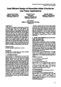
2.1. Circuit Description Our design consists of a 32-bit ripple carry adder in which a 1-bit full adder (see Figure 1) is replicated 32 times with Cin,0 = 0 and Cin,i = Cout,i-1 for i = 1 to 31, where Cin,i and Cout,i are the Carry-In and Carry-Out for the ith full adder, respectively. (b)
The gates are all sized so that each full-adder-circuit provides the same pull-up and pull-down current at the sum output (S) as a unit inverter where the width ratio of PMOS to NMOS in the unit inverter is 2:1. We have also placed 3 unit inverters in parallel with each sum bit to get a fanoutof-3 (FO3) delay. 2.2. Experiments In order to verify our hypothesis, we used extensive HSPICE simulations using a standard 90 nm cell library. All transistors have a minimum length and a minimum width of 120 nm. Experiment 1: Trading Speed for Power In this experiment, we scaled the voltage down while measuring the speed of the circuit for each voltage level. Our goal was to check whether the circuit fails beyond some voltage level or whether it keeps working properly no matter how low the voltage supply gets and as long as we give it enough time to respond.
(c) Figure 1. 1-bit full adder: (a) Schematic, (b) Gate level and (c) Transistor level
Experiment 2: Fixing VDD on Carry Circuit In this experiment, we fixed the voltage level to a high nominal VDD on the carry chain (since it constitutes the critical path) and we fixed the frequency of operation. Then, we started scaling down the voltage on the sum circuits to the point where we lost perfect reliability.
Table 1: Experiment 1 average power and delay VDD(V) 1.2 1 0.8 0.7 0.6 0.5 0.4 0.3 0.25 0.2
Experiment 3: Use of Multi-VDD for Power Reduction We divided the bits of the 32-bit sum into 3 groups (bits [31-22], bits [21-11], bits [10-0]) where we placed the 11 least significant bits at the voltage supply VDD1, the next 11 bits at VDD2 and the 10 most significant bits at VDD3. Inspired by the result of the previous experiment, we kept VDD3 high (at the same voltage as the carry circuit) but we scaled down VDD1 and VDD2.
118
AVG PWR (W) ���������� � ����������� � ����������� ���������� ���������� � ����������� ���������� � ���������� � ���������� �����������
Delay (s) ���������� ���������� � ���������� ���������� ���������� ���������� ���������� ���������� ���������� ����������
Experiment 4: Trading Reliability for Power In this experiment, we removed completely the sum circuit for the 11 least significant bits and measured the additional power savings. 3. RESULTS AND ANALYSIS The results of the first experiment are summarized in Table 1. We simulated the circuit using a worst-case input (one vector is all 0’s while the other vector is all 1’s). The bits that are ‘0’ are simply grounded whereas the bits that are ‘1’ switch to VDD with a 50 ps rise time. To measure the delay, we measured the time from the instant the input reaches 50% of its final value to the output bit to reach 50% of its final value. We took the worst-case delay of the 32 bits as the result. Even at a supply level of 0.2 V, none of the bits failed. Hence, if an application could wait up to ����������� s (this is the worst case delay of a 0.2V) it can consume 40 times less power than if it were to use a supply at 1.2V, while still achieving 100% reliability. Note that trading delay for power is very common in the nanometer era [4, 6]. What we want to emphasize here is the robustness of the adder since it operates with perfect reliability if it was given enough time and this will be the inspiration for our next experiment. We first note that the worst-case delay of a 32-bit adder is given by: ������ � ��������� � ����
(1)
The carry circuit is on the critical path and hence, in order to speed up our circuit we need to make the carry circuit fast. This also tells us that since the sum circuit is not on the critical path, we can relax the constraints on it. This is why we will fix the voltage to a nominal value on the carry circuit (in our case, we fixed it to 0.8V) while we scale the voltage down on the sum circuit only and hence maintaining the performance while gaining in power reduction. The delay at 0.8V (for both carry and sum circuits) for a worst case input is used as the maximum time to wait for the outputs of the other test cases. The results are summarized in Table 2. We stopped scaling the voltage at 0.4V since already 2 of the outputs (most significant bits) were generating erroneous results. From Table 2, we can deduce that going down from 0.8V to 0.6V saves 19% in power consumption.
119
Table 2: Experiment 2 average power VDD (V) 0.8 0.7 0.6 0.5 0.4
AVG Power (W) ���������� ���������� ���������� ���������� ����������
The problem with Experiment 2 was that the most significant bits were being scaled down along with the other bits which made the circuit fail at 0.4V because the most significant bits need to generate their results faster than the others and not much time was given for them to compute correctly. Hence, what we propose is to fix the 10 most significant bits to 0.8V (along with the carry circuit) and simply scale down the rest of the bits. It makes sense to even separate the rest of the bits into 2 parts since the intermediate bits can be given less time than the least significant bits to produce their results. We performed the simulations of this experiment using 33 test cases with random inputs according to a pseudorandom, uniform distribution. The results of Table 3 show the average value of the power consumption over all 33 test cases. The 3 rightmost columns of Table 3 represent the combination of voltage supplies we used in each case. All the cases presented in Table 3 (except for cases X, XII and XIII) showed perfect reliability and hence, we present the errors of the exceptional cases in Table 4. The columns labeled 0 to 21 represent the sum bits 0 to 21 respectively; the sum bits from 22 to 31 are not shown since they all had 100% reliability (for all cases). The percentage in the cells represents the percentile error of each of the bits over our sample of the 33 test cases. Looking carefully at Table 4, it seems that the optimal voltages to use while still achieving perfect reliability are present in Case III which consists of 0.6V on the first 22 bits and 0.8V on the rest of the bits and on the carry circuit. In this case, the results show savings of 58% in power consumption when compared to the power consumption in the standard case, Case I.
Table 3. Experiment 3 Power consumption and voltage settings
Case I Case II Case III Case IV Case V Case VI Case VII Case VIII Case IX Case X Case XI Case XII Case XIII
AVG Power (W) ����������� ����������� ����������� ����������� ����������� ����������� ���������� ����������� ����������� ����������� ����������� ����������� �����������
Bits [0-10] 0.8V 0.6V 0.6V 0.6V 0.5V 0.5V 0.5V 0.4V 0.4V 0.4V 0.3V 0.25V 0.2V
Bits [11-21] 0.8V 0.7V 0.6V 0.4V 0.5V 0.4V 0.3V 0.4V 0.3V 0.25V 0.3V 0.25V 0.2V
Bits [12…31] 0.8V 0.8V 0.8V 0.8V 0.8V 0.8V 0.8V 0.8V 0.8V 0.8V 0.8V 0.8V 0.8V
Table 4. Experiment 3 Percentage errors 0
1
2
3
4
5
6
7
8
9
10
Case X Case XII Case XIII
0% 0% 64%
0% 0% 52%
0% 0% 52%
0% 0% 55%
0% 0% 48%
0% 0% 55%
3% 3% 52%
3% 3% 55%
3% 3% 52%
0% 0% 61%
0% 0% 45%
Case X Case XII Case XIII
11 0% 3% 58%
12 0% 0% 61%
13 0% 3% 61%
14 0% 3% 45%
15 0% 6% 55%
16 0% 0% 39%
17 0% 3% 52%
18 0% 0% 67%
19 0% 0% 33%
20 0% 6% 58%
21 0% 6% 55%
In the last experiment, we completely removed the sum circuits for the 11 least significant bits. The results for this experiment are summarized in Table 5. We simulated the circuit using 33 inputs that are pseudo-randomly generated, and uniformly distributed. We fixed in this experiment the voltage on the carry chain and on the 10 most significant bits at 0.8V while we scaled down the voltage on the 11 intermediate bits.
Finally, we note that some applications like the ones discussed in [4] and [5], are error tolerant up to some percentage (usually lower than 10%) and hence the results in Table 4 would be useful for such applications. Obviously, a more detailed study should be done about the exact error that the adder circuit produces when it comes to adding two binary numbers, which will be a prospect for future study. Cases X and XII have low percentages of errors and hence they are far more accurate than Case XIII, but the power savings in Case XIII are far greater. In Case XII, we get 148% savings in power while in Case XIII, we get 168% (both are compared to Case I, the standard case). An important conclusion to draw at this point is that we are able to obtain substantial savings in power at a reasonable loss in accuracy.
Table 5. Experiment 4 average power VDD (V) Case 1: 0.8 Case 2: 0.7 Case 3: 0.6 Case 4: 0.5 Case 5: 0.4 Case 6: 0.3
120
AVG Power (W) ����������� ����������� ����������� ����������� ����������� �����������
REFERENCES
Comparing Case 1 and Case I (from experiment 3), we realize that we have additional savings of 41% in power consumption. Also, comparing Case 3 with Case III (from experiment 3), we have 26% additional savings in power consumption.
[1] R. Gonzalez, B. M. Gordon, and M. A. Horowitz, “Supply and Threshold Voltage Scaling for Low Power CMOS,” IEEE Journal of Solid-State Circuits, vol. 32, no. 8, August 1997. [2] M.Á. Gonzalez, “Low Power Design Techniques for Embedded Systems, Dynamic Power Management,” found at: http://www.iti.unistuttgart.de/~rainer/Lehre/SOCfCA01/Present ation10/Seminar.pdf
4. SUMMARY AND CONCLUSIONS There are many ways to reduce the power consumption of a circuit. One of them is voltage scaling, which is what we exploited in this paper. The results showed that the voltage supply level can be brought down to 0.2 V, and yet, the adder will give a correct result, as long as we give it enough time to produce those results. However, if there is a constraint on the delay, we would have to resort to multi-VDD supplies. The voltage on the critical path of the circuit (which is the carry circuit in this case) should remain at its nominal level, while we can scale the voltage down on the other paths (the sum circuit in this case). It is important to avoid errors in the most significant bits and hence we should not scale the voltage down on the most-significant sum-bit circuits. This method of scaling enables us to trade reliability for power, but in such a way as to only lose reliability in the least significant bits, with benefits reaching 58% in power savings while achieving perfect reliability, and 168% if we can tolerate some errors. Finally, by eliminating the sum circuit for the 11 least significant bits, we can reach 41% additional power savings. Finally, we note that since multi-VDD supplies are becoming readily available in low-power chips, the additional overhead of using such supplies is minimal.
[3] A.P. Chandrakasan, S.Sheng, and R.W. Brodersen, “LowPower CMOS Digital Design,” IEEE Journal of Solid-State Circuits”, vol. 27, no. 4, April 1992. [4] M. Hamada, Y.Ootaguro, and T. Kuroda, “Utilizing Surplus Timing for Power Reduction,” IEEE 2001 Custom Integrated Circuits Conference, 2001, pp. 89-92. [5] Q. Ma and E.F. Y. Young, “Voltage Island-Driven Floor planning,” IEEE/ACM International Conference on Computeraided design, 2007, pp. 1401 -1404. [6] S. Lin, H. Yang, R. Luo, “A Novel Low Power Interface Circuit Design Technique for Multiple Voltage Islands Scheme,” IEEE International Symposium on Circuits and Systems, 27-30 May 2007, pp. 1401-1404. [7] S. Narayanan, J. Sartori, R. Kumar, and D. L. Jones, “Scalable Stochastic Processors,” Design, Automation & Test in Europe Conference & Exhibition, 2010, pp. 335 – 338. [8] P. S. Duggirala, S. Mitra, R. Kumar and D. Glazeski, “On the Theory of Stochastic Processors,” Seventh International Conference on the Quantitative Evaluation of Systems, 2010, pp. 292 – 301. [9] Roundtable Discussion, “Designing Chips without Guarantees,” IEEE Design & Test of Computers, Vol. 27, No. 5, pp. 60-67, 2010.
5. FUTURE WORK Future work includes extending the number of bits in the ripple carry adder up to 1028, and investigate the power savings in a larger circuit. Also, the same strategy of using multiple voltage supplies to balance the critical path along with the other paths will be applied to other circuits starting with different adder topologies. 6. ACKNOWLEDGMENTS This work was supported by Intel’s Middle East Energy Efficiency Research (MER).
121