order for reading the coefficients from the ROM and the other .... h_reg. 4% rom. 0% c) TDF/norm d) TDF/min. Figure 3: Distribution of power consumption for the.
Low Power FIR Filter Implementations Based on Coefficient Ordering Algorithm A. T. Erdogan1 and T. Arslan1,2 1 University of Edinburgh, School of Engineering and Electronics, Edinburgh, EH9 3JL, UK 2 The Institute for System Level Integration, Alba Centre, Alba Campus, Livingston, EH54 7EG, UK {ate,arslan}@ee.ed.ac.uk Abstract The authors present a number of low power FIR filter implementations. The implementations are based on processing coefficients in a non-conventional order using both direct form and transpose direct form realisation of FIR filters. The paper describes the overall filter architecture of each implementation and their key components. An overall power reduction of up to 34% is reported as compared to a conventional filter implementation. A power profile of the main contributing components in each implementation is also provided.
1. Introduction One of the fastest growing areas in the computing industry is the provision of high throughput DSP systems in a portable form [1]. With the advent of SoC technology, DSP algorithms such as FIR filters are being prototyped as parameterisable cores which could be embedded within the SoC platform. For high performance low power applications, there is a continuous demand for DSP cores, which provide high throughput while minimising power consumption. In recent years a number of techniques have been proposed for low power implementation of FIR filters. These include the following: use of differential coefficients [2], multirate architectures [3], and dynamic adjustment of filter order [4]. A number of researchers including the authors have investigated the use of coefficient ordering for low power implementation of FIR filters [5-6]. However, most reported work considers power reduction at multiplier inputs or within the multiplier unit alone. In this paper, the authors present a number of low power FIR filter implementations. The implementations are based on processing coefficients in a non-conventional order using both direct form and transpose direct form FIR filters. The paper describes the overall filter architecture of each implementation and their key components. An overall power reduction of up to 34% is reported as compared to a conventional filter implementation. A power profile of the main contributing components in each implementation is also provided.
2. Implementation Two common methods of realizing FIR filters are the direct form (DF) and the transpose direct form (TDF). In the DF realization of the filter, there are delay units between multipliers. This implies that the present input, x(n), and N-1 previous samples of the input, that is x(n-1) to x[n-(N-1)], are applied to each multiplier input and the outputs of these multipliers are summed together to form the filter output y(n). In the TDF,
however, delay units are placed between adders so that the multipliers can be fed simultaneously. A DF filter is implemented such that at each clock cycle a new data sample and the corresponding filter coefficient are applied to the multiplier inputs. This continuous change at both inputs will cause a high level of switching activity within the multiplier, and hence leading to higher power consumption. Using a TDF realization, however, the switching activity at data inputs of the multiplier is significantly reduced since the data input remains unchanged for a significant number of multiplication operations. This results in a considerable reduction in switching activity within the multiplier circuit and consequently leads to less power consumption than the DF realization. A further reduction in switching activity within the multiplier section of both DF and TDF filters can be achieved by implementing the filters such that respective data samples are multiplied with filter coefficients in a non-sequential order [5]. This results in reducing the switching activity at both multiplier inputs. A block diagram of the DF FIR filter implementation is illustrated in Figure 1. There main blocks can be identified as the coefficient memory, the data memory, and the multiplyaccumulator (MAC). The coefficient memory consists of a ROM, a look-up table (LUT), an address counter, and a data multiplexer. A demultiplexer, a ring memory (data_ring), a multiplexer, and a write and read address counter are the subblocks of the data memory. The data_ring is latch-based and realized in the form of a circular buffer for reducing its power consumption. The MAC module contains a multiplier, an adder and an accumulator register (accu). The controller module is not shown in this diagram. This filter architecture can also be used for filter implementations where filter coefficients are processed in a non-sequential manner for reduced switching activity at the coefficient input of the multiplier, as described earlier. This involves creating two LUTs, one indicating the new coefficient order for reading the coefficients from the ROM and the other indicating the corresponding data sample to be read from the RAM. The TDF FIR filter architecture, shown in Figure 2, looks very similar to the DF FIR filter architecture. However, in this case x data input is directly connected to the multiplier and hence the data_ring is no longer required for storing x data samples. On the other hand, the accumulator register (accu) in DF filter is replaced with a set of registers (accu_ring) in TDF filter for storing each multiply-add output into a different register. In addition, this accumulator memory (accu_ring) has an increased wordlength (i.e., N*2w) compared to the DF FIR filter (i.e., Nw). Clearly, this reduces the switching activity at the data input of the multiplier (since data sample remains
Proceedings of the IEEE Computer Society Annual Symposium on VLSI Emerging Trends in VLSI Systems Design (ISVLSI’04) 0-7695-2097-9/04 $20.00 © 2004 IEEE
Nw Nw
N:1w
N:1w
x h
ROM
h
ROM ROM LUT b_addr h_addr 1:Nw
Nw
f
f
f
α
β
γ
f
f
f/N
α
β
γ
LUT LUT h_addr
* +
*
N:1w +
1:N*2w accu
f/N
r_addr
f
data_ring
r
2w bit
e a leb at LUT
x
w_addr
f
+
N*2w
y LUT write w_addr
f
+
accu_ring accu_ring
read r_addr
y
Figure 1: DF FIR filter architecture. unchanged for N clock cycles), with the expense of increased memory size. Similar to the DF filter case, the coefficients can be processed in a non-sequential order for reducing switching activity at the coefficient input of the multiplier. This can easily be achieved with the use of LUTs for generating read addresses for ROM, and read/write addresses for accu_ring. However, this will require further increase in accu_ring memory size. This increase will depend on the new coefficient order (more detail on this issue can be found in [5]). Terms used to illustrate the complexity of the different cells in these diagrams are as follows: • The width of the different cells such as counters and multiplexers are defined using the number of coefficients (N) and the wordlength (w). For example, Nw indicates a Nxw-bit memory, and N:1w is a N-to-1 (w-bit) multiplexer. • Symbols such as f of f/N indicate the activity of a node. A node with activity f/N is therefore changing every N clock cycles. • The LUTs are used for the implementation of coefficient ordering.
3. Simulations and results
N:1*2w
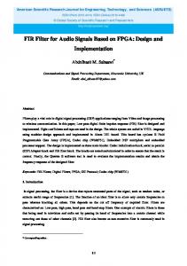
Figure 2: TDF FIR filter architecture. layouts was then used by the Synopsys DesignPower™ tool to compute power consumptions for the different FIR filter implementations, assuming a clock rate of 10 MHz and a supply voltage of 3 Volt. The power analysis results for each implementation are presented in Figure 3 and Table 1 for a 24-tap linear phase lowpass filter using 16-bit data/coefficient wordlength and a low power Booth multiplier described in [7]. According to Figure 3, for DF based implementations 73-80% of the total power is consumed by MAC, 8-11% by CTRL the remaining 12-16% by the rest of the filter components. Whereas, for TDF based implementations RAM power increases to 21-34%, MAC power decreases to 45-59%, CTRL consumes 8-13% and the remaining 8-12% of the total power is consumed by the rest of the components. round 0%
h_reg 2%
rom 1% ram 3% ctrl 8%
x_reg 5% o_reg 1%
round 0% rom 0%
h_reg 2%
x_reg 6%
o_reg 2%
ram 6% ctrl 11%
A number of cores were designed and implemented based on the processing of coefficients in their normal order (norm) and in a non-sequential order (min) for minimum Hamming distance between successive filter coefficients as described in section II. The cores were implemented for both DF and TDF filter realizations. Therefore, the implemented filters were named as DF/norm, DF/min, TDF/norm, and TDF/min based on the filter structure and coefficient order employed in each implementation. The cores were designed using Verilog HDL and then synthesized using Ambit BuildGates targeting a 0.35u standard cell CMOS technology library. A maximum circuit delay of 35ns has been defined for all the cores. A layout for each core was generated with the Envisia™ Silicon Ensemble™ place-and-route software. SDF back-annotated post-layout gatelevel simulations were performed for randomly generated data samples using Verilog-XL™ simulator. The resulting switching activity information and the capacitive loads extracted from the
mac 73%
mac 80%
a) DF/norm round 1% rom 1%
h_reg 6%
b) DF/min
x_reg 2% o_reg 2%
rom 0%
round 0%
h_reg 4% x_reg 2% o_reg 2% mac 45%
ram 21%
mac 59%
ram 34%
ctrl 8%
ctrl 13%
c) TDF/norm
d) TDF/min
Figure 3: Distribution of power consumption for the different FIR filter implementations.
Proceedings of the IEEE Computer Society Annual Symposium on VLSI Emerging Trends in VLSI Systems Design (ISVLSI’04) 0-7695-2097-9/04 $20.00 © 2004 IEEE
Table 1: Power consumption Cell
DF/norm DF/min
%
TDF/norm
%
TDF/min
%
9
6.416
4.796
25
3.513
45
2.354
63
8
ctrl
0.607
0.688
-13
0.470
23
0.700
-15
7
o_reg
ram
0.261
0.394
-51
1.229
-371
1.817
-596
6
x_reg
power [mW]
mac
h_reg 5
round
4
rom
rom
0.044
0.022
50
0.045
-2
0.024
45
round
0.012
0.012
0
0.037
-208
0.020
-67
h_reg
0.171
0.129
25
0.342
-100
0.198
-16
3
x_reg
0.394
0.373
5
0.102
74
0.103
74
2
0.101
0.101
0
0.101
0
0.103
-2
Total
8.006
6.515
19
5.839
27
5.319
34
Table 1 provides the power consumed by each filter component and the percentage reduction/increase in the power consumption by comparing DF/min, TDF/norm and TDF/min against DF/norm implementation. As can be clearly seen, MAC power is decreased by 25%, 45% and 63% for DF/min, TDF/norm, and TDF/min respectively. These reductions are directly related to the switching activity reduction at one (coefficient input in the case of DF/min and data input in the case of TDF/norm) or both multiplier inputs (in the case of TDF/min). The increase in RAM power for TDF implementations is mainly due to the increased RAM size as well as increased memory accesses. DF implementations involve one read access each clock cycle, and one write access every N clock cycles (for a N-tap filter). Whereas, TDF implementations require both read and write accesses to the memory every clock cycle. Therefore, RAM power for TDF/norm increases significantly compared to the RAM power for DF/norm. RAM power for TDF/min is even higher due to the further increase in RAM size (as explained in Section 2). Clearly, this increased RAM size represents both area and power overheads for TDF implementations. Figure 4 depicts the total power consumption for each FIR filter implementation. It is clear that although RAM power increased significantly for TDF implementations, the best overall power reductions are still obtained by TDF implementations (27% by TDF/norm and 34% by TDF/min). However, as shown in Figure 5, these power savings come with an increase in area (26% for TDF/norm and 56% for TDF/min). On the other hand, DF/min achieves 19% overall power saving with no area overhead.
4. Conclusions The authors have presented a number of low power FIR filter implementations. Coefficient ordering was applied to both DF and TDF filter structures. Until now researchers in the literature have studied the effect of ordering coefficients focusing on the multiplier without considering the overall filter implementations. Results were demonstrated indicating an overall power reduction of up to 34% with up to 56% area overhead in the case of a TDF filter structure with coefficient ordering. However, when coefficient ordering was applied to a DF filter structure an overall 19% power reduction was achieved without incurring any area overhead.
ctrl mac
1 0 DF/norm
DF/min
TDF/norm
TDF/min
Figure 4: Total power consumption.
40 30 20 10 % saving
o_reg
ram
0 Power
-10
Area -20 -30 -40 -50 -60 DF/min
TDF/norm
TDF/min
Figure 5: Power and area comparison.
5. References [1] I.S. Abu-Khater, A. Bellaouar, M.I. Elmasry: “Circuit Techniques for CMOS Low-Power High-Performance Multipliers”, IEEE Journal of Solid-State Circuits, vol. 31, no. 10, pp. 1535-1546, Oct. 1996. [2] N. Sankarayya, K. Roy, D. Bhattacharya: “Algorithms for Low Power and High Speed FIR Filter Realisation Using Differential Coefficients”, IEEE Trans. on Circuits and Systems-II, 1997, vol. 44, no. 6, pp. 488-497. [3] M. Mehendale, S.D. Sherlekar, G. Venkatesh: “Low Power Realisation of FIR Filters Using Multirate Architectures”, 9th Int. Conf. on VLSI Design, pp. 370-375, Jan. 1996. [4] J.T. Ludwig, S.H. Nawab, A.P. Chandrakasan: “Low Power Digital Filtering Using Approximate Processing”, IEEE J. of Solid-State Circuits, vol. 31, pp. 395 399, Mar. 1996. [5] A.T. Erdogan and T. Arslan: “On the Low Power Implementation of FIR Filtering Structures on Single Multiplier DSPs”, IEEE Trans. on Circuits and Systems II, vol. 49, no. 3, March 2002, pp. 223-229. [6] M. Mehendale, S.D. Sherlekar, G. Venkatesh: “Low-Power Realization of FIR Filters on Programmable DSPs”, IEEE Trans. on VLSI Systems, vol.6, no.4, pp.546-553, Dec. 1998. [7] R. Fried: “Minimizing energy dissipation in high-speed multipliers”, IEEE Symposium on Low Power Electronics and Design, ISLPED’97, pp. 214-219.
Proceedings of the IEEE Computer Society Annual Symposium on VLSI Emerging Trends in VLSI Systems Design (ISVLSI’04) 0-7695-2097-9/04 $20.00 © 2004 IEEE