MODELING AND CHARACTERIZATION OF LOGARITHMIC CMOS ACTIVE PIXEL SENSORS
Muahel Tabet, Nick Tu, and Richard Hornsey
[email protected] Department of Electrical and Computer Engineering, University of Waterloo, 200 University Avenue West, Waterloo, Ontario, N2L 3G1 Canada
ABSTRACT We present a detailed analysis of logarithmic active pixel sensors (Log-APS) to be used in CMOS imagers for real-time on-chip motion detection. Based on an equivalent circuit model for CMOS-compatible photodiodes, an HSPICE simulation has been used to characterize different configurations of these sensors under various conditions of light intensities and switching speeds. These investigations are supported by the experimental results obtained from the chip fabricated with standard 0.5 µm CMOS technology. It is concluded that more robust on-chip motion detection in CMOS imagers can be achieved with careful design of its Log-APS photocircuits that consider the issues discussed here.
Tabet et al.
Modeling and Characterization of Logarithmic CMOS Active Pixel Sensors
1
I.
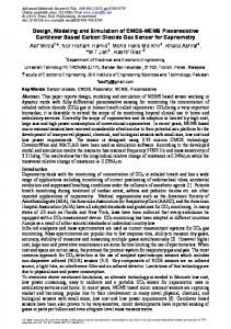
INTRODUCTION Logarithmic active pixel sensors (Log-APS), shown in Fig. 1, have been the basic
photocircuit of many CMOS imagers,
1-3
because of their smaller size, and large optical
dynamic range. Their "logarithmic" compression arises from the saturated sub-threshold operation of their MOS diode(s) [diode connected MOSFET(s)], which continuously performs logarithmic photocurrent-to-voltage conversion. This also facilitates random temporal access to the imaging array. Accordingly, these sensors gained potential to be used in applications such as the on-chip real-time motion detection of interest here. The motion detection is performed by continuous (temporal) differentiation of the light intensity. This is accomplished by differentiating pixel output voltage (which is related to the incident light intensity) using analog differentiators. For the intended application here, industrial inspection (interiors with controlled lighting), there is no optical dynamic range constraint (especially when using Log-APS) and the rate of change of light intensity is directly related to the motion. The main issues in this case are the sensitivity of the Log-APS pixel and its speed of response, since the sensitivity of the differentiators is usually limited, especially in the presence of digital noise. In contrast, this kind of photocircuits suffers from an extreme compression due to its logarithmic response that can limit its ability to detect small changes in light intensity, especially at low rates of change of light intensity (slow motion). Therefore, these photocircuits have to be studied and analyzed carefully under different conditions of light intensity (levels and speed of change) in order to optimize their performance for motion detection. 4, 5 In this paper, we present HSPICE 6 simulations for a variety of configurations of CMOS Log-APS. Supporting experimental results are also presented where appropriate.
Tabet et al.
Modeling and Characterization of Logarithmic CMOS Active Pixel Sensors
2
All experimental results are obtained from the prototype imager chip fabricated with standard 0.5µm CMOS digital process. This imager consist of an array of a 64 x 64 pixels, with pixel pitch of 30µm. Each pixel (as shown in Fig. 1) contains a photodiode and three transistors, which result in a fill-factor (defined as the fraction of the pixel area that is photosensitive) of about 60%. The chip also contains digital circuits for timing and control. Section II describes the electrical sensitivity analysis and results. In section III, we investigate the speed of response, where the optical modulation frequency response was used to determine the switching speed of these sensors. Finally, results are discussed and concluding remarks are made.
II. ELECTRICAL SENSITIVITY ANALYSIS A typical response of the Log-APS to light intensity is shown in Fig. 2. The photocircuit exhibits a wide optical dynamic range; ~5 orders of magnitude change in light intensity results in less than 250-mV change in output voltage. This is in contrast to linear active pixel sensors where output voltage swing (~1.2 V) is typically the limiting factor for dynamic range. Simulated results using HSPICE are also shown in the same figure, showing a good agreement between simulated and measured results. In these simulations, we used MOSFET model level 13 (which considers all associated parasitic capacitances) 6, and a suitable equivalent circuit model
7, 8
for the
CMOS-compatible photodiode. The photodiode model parameters are either selected from the standard HP 0.5µm CMOS technology data used in the fabrication of the chip or extracted from measurements. Moreover, to include the body effect in our simulation, all
Tabet et al.
Modeling and Characterization of Logarithmic CMOS Active Pixel Sensors
3
bodies of MOSFETs are connected to the substrate (not shown in the figures for the sake of simplicity) as usually the case in integrated circuits. There are several other configurations of Log-APS,
1-5, 9
however they can all be
classified in two main categories, either conventional or inverted. The difference between these two categories is in their output responses as shown in Fig. 3, and in the respective locations of their MOS diode(s) and the photodiode as shown in the insets of Fig. 4 and Fig. 5. The two kinds have qualitatively a mirror-image response with the conventional having a descending response to higher light intensity, and inverted have an ascending one. Also, both kinds exhibit the same amount of logarithmic compression, i.e. they have the same electrical sensitivity in mV/[W/m2], as shown in Fig. 3. In both configurations, the photosensor can be either photodiode or phototransistor, and can be implemented using one, two, or three (series) MOS diodes. Increasing the number of MOS diodes will reduce the compression (thus increase the electrical sensitivity), as illustrated in Fig. 4 and Fig. 5. The effect is more pronounced in conventional Log-APS than inverted pixels, as shown. This is attributed to the circuit configuration of the conventional Log-APS which is more affected by the body-effect than the inverted one if extra MOS diodes are added. The reason is due to the fact that the source(s) of the added MOS diode(s) is always in higher potential in conventional LogAPS than those in inverted ones. This in turn leads to larger changes in the threshold voltages, thus, larger resistance added to the circuit. In spite of that, conventional LogAPS are more suitable for motion detection applications as they allow sensitivity to be increased by reducing the compression.
Tabet et al.
Modeling and Characterization of Logarithmic CMOS Active Pixel Sensors
4
III. OPTICAL MODULATION FREQUENCY RESPONSE ANALYSIS In the operation of Log-APS, the photodiode capacitance, and other associated parasitic capacitances, are charged or discharged by means of the photocurrent. This can limit the speed of response, especially during a transition from high- to low- illumination, when the final photocurrent can be as low as 10 fA. One way to measure the speed of response of Log-APS is by using the "optical modulation frequency response" as a measure of the speed of response. In this method, the electrical frequency response of the pixel is measured for optical ac inputs. The term "optical modulation" is used here to distinguish it from the so-called "spectral response". By calculating the 3-dB frequency from the measured frequency response, one can estimate the range of speeds under which the Log-APS can perform. This approach can be a very reliable technique especially for the motion detection applications. However, to our knowledge, there has been little work done on studying the pixel response speed using this method .10 The optical modulation frequency response was measured using red laser diode (670 nm) modulated with a square wave to give a peak output of ~ 2 mW/cm2, with frequency range 200 Hz to 1M Hz. Figure 6 shows that the response of conventional pixel (size 30µm) has 3-dB cut-off frequency of about 97.5 kHz. This corresponds to maximum focal plane speed of ~ 6m/s; the corresponding speed of an imaged object depends on the optics of the system. Simulated results obtained using HSPICE are also depicted in the same figure. Comparison shows a good agreement between measured and simulated cut-off frequencies.
Tabet et al.
Modeling and Characterization of Logarithmic CMOS Active Pixel Sensors
5
Simulation results presented above showed that the electrical sensitivity of the conventional Log-APS can be improved (as shown in Fig. 4) by increasing the number of the MOS diodes in the pixel. However, this improvement can only be achieved on the expense of the speed of the response as illustrated in Fig. 7. The higher the sensitivity the lower the 3-dB frequency (or maximum speed) of the optical modulation frequency response of Log-APS and vise-versa. There is thus a tradeoff between pixel sensitivity and frequency response, arising because the same photocurrent must cause a larger voltage swing at the gate of the source-follower. Another interesting result in this context (shown in Fig. 8) is the effect of the ambient (dc) illumination on the speed of response. This is a very important issue especially at low ambient illumination where the low photocurrents generated tend to slow the charge/discharge mechanism of diode capacitance and other associated parasitic capacitances. This indicates that the speed of response to a moving object will be lower at lower illumination levels.
IV. DISCUSSION AND CONCLUSION CMOS Log-APS performance has been analyzed in terms of electrical sensitivity and speed of response. Results showed a good agreement between simulation and measurements (Fig. 2, and Fig. 6). These results suggest that the conventional Log-APS have superiority over the inverted one, because it has higher output voltage levels (especially at low light intensity levels) compared to those of the inverted (refer to Fig. 3). Therefore conventional pixels expected to have higher output signal-to-noise-ratio in this early (and important) stage of
Tabet et al.
Modeling and Characterization of Logarithmic CMOS Active Pixel Sensors
6
signal processing than the inverted ones. Moreover, the electrical sensitivity of the conventional structure can be improved by increasing the number of the MOS diodes in the pixel (Fig. 4). However, this action has some drawbacks; it will not only decrease the fill-factor but will also reduce the speeds of response, as predicted by HSPICE simulation (see Fig. 7). Therefore there is a tradeoff between the electrical sensitivity of the pixel and its speed of response. For the present application, motion detection, both figures of merit are important. Accordingly, the choice of conventional pixel with two MOS diodes would be a good compromise. In this case we sacrifice some speed and fill-factor for the sake of more electrical sensitivity. Another important result is the effect of the ambient illumination on the speed of response of the pixel, which shows that for low light intensity the speed of response (3dB-frequency) will be reduced (refer to Fig. 8). Thus we should take this effect in our consideration when designing for low light intensity illumination, especially in application where speed of response is vital. Its is concluded that a more robust on-chip motion detection in CMOS imagers with Log-APS as photocircuit can be achieved with careful designs that consider all issues discussed here.
Tabet et al.
Modeling and Characterization of Logarithmic CMOS Active Pixel Sensors
7
REFERENCES 1
N. Ricquier and B. Dierickx, IEEE Workshop CCD's and Advanced Image Sensors,
Dana Point, CA, Apr. 20-21, 1995. 2
B. Dierickx, D. Scheffer, G. Meynants, W. Ogiers, and J. Vlummens, in Europto Conf.
Advanced Focal Plane Array and Electronic Cameras, Berlin, Germany, Oct. 9-10, 1996, pp. 1-5. 3
D. Scheffer, B. Dierickx, and G. Meynants, IEEE Trans. Electron Devices ED-44, 1716
(1997). 4
A. Moini, A. Bouzerdoum, A. Yakovleff, D. Abbott, O. Kim, K. Eshraghian and R.E.
Bogner, The Proceedings of 1993 Int. Symposium on VLSI Technology, Systems, and Applications, 1993, p. 283. 5
A. Yakovleff, A. Moini, J. Analog Integrated Circuits and Signal Processing 15, 183
(1998). 6
HSPICE user’s Manual, (Meta-Software, Campbell, 1992). Vol. 2 & 3.
7
E. Uiga, Optoelectronics (Prentice Hall, New Jersey, 1995).
8
S. M. Sze, Physics of Semiconductor Devices (Wiley, New York, 1981).
9
C. Mead, Analog VLSI and Neural Systems (Addison-Wesley, New York, 1989).
10
J. Huppertz et al., IEEE Workshop on Charge-Coupled Devices and Advanced image
Sensors, Bruges, Belgium, June 5-7, 1997.
Tabet et al.
Modeling and Characterization of Logarithmic CMOS Active Pixel Sensors
8
FIGURE CAPTIONS Figure 1. The conventional Log-APS with one MOS diode M1 connected to the column data bus via the source-follower M2 and the row select switch M3. All MOSFETs bodies are connected to the substrate. Figure 2. Typical response of Log-APS to light intensity (at node N2 in Fig. 1). Simulated results obtained using HSPICE modeling are shown for comparison. Figure 3. Comparison between responses (at N1 in Fig. 1) of the conventional and inverted LogAPS using HSPICE simulation. Figure 4. Comparison of the responses (at N1 in Fig. 1) of conventional pixels with different number of MOS diodes using HSPICE simulation. All MOSFETs bodies are connected to the substrate. Figure 5. Comparison of the responses (at N1 in Fig. 1) of inverted pixels with different number of MOS diodes using HSPICE simulation. All MOSFETs bodies are connected to the substrate. Figure 6. Comparison between measured and simulated optical modulation frequency response for Log-APS, at node N2 in Fig. 1.
Tabet et al.
Modeling and Characterization of Logarithmic CMOS Active Pixel Sensors
9
Figure 7. Comparison of the simulated optical modulation frequency responses of the conventional Log-APS with one, two and three MOS diodes, at node N2 in Fig. 1. Figure 8. Simulated ambient illumination effect on 3-dB frequency for Log-APS (Conventional configuration, at node N2 in Fig. 1).
Tabet et al.
Modeling and Characterization of Logarithmic CMOS Active Pixel Sensors
10
Tabet et al.
Modeling and Characterization of Logarithmic CMOS Active Pixel Sensors
Figure 1.
Column Bus
VDD
Pixel Borders
M1
VDD
Row
N1
Light IPhoto
M2 N2
N+ P- substrate
M3 Vbias Current source load
M2
Tabet et al.
Modeling and Characterization of Logarithmic CMOS Active Pixel Sensors
Figure 2.
Output voltage (V)
3.04 3 2.96 2.92 2.88 2.84 2.8 0.0001
Measurement Simulation
0.001
0.01
0.1
Light intensity (W/m2)
1
10
Tabet et al.
Modeling and Characterization of Logarithmic CMOS Active Pixel Sensors
4.25
0.6
4.2
0.5
4.15
0.4
4.1 0.3 4.05 0.2
4 Conventional Inverted
3.95
0.1
3.9 0.0001
0 0.001
0.01
0.1
1
Light intensity (W/m2)
10
100
Output voltage (V)
Output voltage (V)
Figure 3.
Tabet et al.
Modeling and Characterization of Logarithmic CMOS Active Pixel Sensors
Figure 4.
Normalized output voltage
1.05 1 0.95 0.9
VDD M1 Light
Vo IPhoto
0.85 PD
0.8 0.75
1 MOS-diode 2 MOS-diodes 3 MOS-diodes
0.7 0.0001 0.001
0.01
0.1
1
10
Light intensity (W/m2)
100
1000
Tabet et al.
Modeling and Characterization of Logarithmic CMOS Active Pixel Sensors
Figure 5.
Normalized output voltage
3.5 3
Light VDD IPhoto
PD 2.5
M1
Vo
2 1.5
1 MOS-diode 2 MOS-diodes 3 MOS-diodes
1 0.5 0.0001
0.001
0.01
0.1
1
10 2
Light intensity (W/m )
100
1000
Tabet et al.
Modeling and Characterization of Logarithmic CMOS Active Pixel Sensors
Figure 6.
3
Attenuation (dB)
-3
-9
-15
-21
Simulation Measurement
-27 100
1000
10000
Frequency (Hz)
100000
1000000
Tabet et al.
Modeling and Characterization of Logarithmic CMOS Active Pixel Sensors
Figure 7.
6
Attenuation (dB)
-3 1 MOS Diode
-12 -21 -30
2 MOS Diodes
-39 -48
3 MOS Diodes
-57 1.E+03
1.E+04
1.E+05
1.E+06
Frequency (Hz)
1.E+07
1.E+08
Tabet et al.
Modeling and Characterization of Logarithmic CMOS Active Pixel Sensors
Figure 8.
3 d B -freq u en cy (H z)
1 .E + 8
1 .E + 7
1 .E + 6
1 .E + 5
1 .E + 4 1 .E -1
1 .E + 0
1 .E + 1
1 .E + 2
1 .E + 3
1 .E + 4
A m b ie n t lig h t in te n sity (W /m 2 )
1 .E + 5
Tabet et al.
Modeling and Characterization of Logarithmic CMOS Active Pixel Sensors
Figure 1.
Column Bus
VDD
Pixel Borders
M1
VDD
Row
N1
Light IPhoto
M2 N2
N+ P- substrate
M3 Vbias Current source load
M2
Tabet et al.
Modeling and Characterization of Logarithmic CMOS Active Pixel Sensors
Figure 2.
Output voltage (V)
3.04 3 2.96 2.92 2.88 2.84 2.8 0.0001
Measurement Simulation
0.001
0.01
0.1
Light intensity (W/m2)
1
10
Tabet et al.
Modeling and Characterization of Logarithmic CMOS Active Pixel Sensors
4.25
0.6
4.2
0.5
4.15
0.4
4.1 0.3 4.05 0.2
4 Conventional Inverted
3.95
0.1
3.9 0.0001
0 0.001
0.01
0.1
1
Light intensity (W/m2)
10
100
Output voltage (V)
Output voltage (V)
Figure 3.
Tabet et al.
Modeling and Characterization of Logarithmic CMOS Active Pixel Sensors
Figure 4.
Normalized output voltage
1.05 1 0.95 0.9
VDD M1 Light
Vo IPhoto
0.85 PD
0.8 0.75
1 MOS-diode 2 MOS-diodes 3 MOS-diodes
0.7 0.0001 0.001
0.01
0.1
1
10
Light intensity (W/m2)
100
1000
Tabet et al.
Modeling and Characterization of Logarithmic CMOS Active Pixel Sensors
Figure 5.
Normalized output voltage
3.5 3
Light VDD IPhoto
PD 2.5
M1
Vo
2 1.5
1 MOS-diode 2 MOS-diodes 3 MOS-diodes
1 0.5 0.0001
0.001
0.01
0.1
1
10 2
Light intensity (W/m )
100
1000
Tabet et al.
Modeling and Characterization of Logarithmic CMOS Active Pixel Sensors
Figure 6.
3
Attenuation (dB)
-3
-9
-15
-21
Simulation Measurement
-27 100
1000
10000
Frequency (Hz)
100000
1000000
Tabet et al.
Modeling and Characterization of Logarithmic CMOS Active Pixel Sensors
Figure 7.
6
Attenuation (dB)
-3 1 MOS Diode
-12 -21 -30
2 MOS Diodes
-39 -48
3 MOS Diodes
-57 1.E+03
1.E+04
1.E+05
1.E+06
Frequency (Hz)
1.E+07
1.E+08
Tabet et al.
Modeling and Characterization of Logarithmic CMOS Active Pixel Sensors
Figure 8.
3 d B -freq u en cy (H z)
1 .E + 8
1 .E + 7
1 .E + 6
1 .E + 5
1 .E + 4 1 .E -1
1 .E + 0
1 .E + 1
1 .E + 2
1 .E + 3
1 .E + 4
A m b ie n t lig h t in te n sity (W /m 2 )
1 .E + 5