Proceedings of COBEM 2011 Copyright © 2011 by ABCM
st
21 Brazilian Congress of Mechanical Engineering October 24-28, 2011, Natal, RN, Brazil
MODELING, SIMULATION AND FABRICATION OF A MEMS-BASED ELECTROSTATIC CAPACITIVE EFFECT – CMUT: FOR GENERATION AND RECEPTION OF ACOUSTIC WAVES. Victor Inacio de Oliveira,
[email protected] Escola Politécnica da Universidade de São Paulo, Av. Prof. Mello Moraes, 2231 – São Paulo - SP Escola Senai “Jorge Mahfuz”, Rua Jerônimo Telles Jr., 125 – São Paulo - SP
Ricardo Cury Ibrahim,
[email protected] Delson Torikai,
[email protected] Bruno Luis Soares de Lima,
[email protected] Lucas G. Dias Mendonça,
[email protected] Escola Politécnica da Universidade de São Paulo, Av. Prof. Mello Moraes, 2231 – São Paulo - SP
Maria Helena de Oliveira Piazzeta,
[email protected] Angelo Luiz Gobbi,
[email protected] Laboratório Nacional de Luz Sincontron (LNLS), Rua Giuseppe Máximo Scolfaro, 10.000 Pólo II de Alta Tecnologia Campinas - SP
Abstract. Micro Electro-Mechanical Systems (MEMS) are becoming essential to modern life. There are many applications of these devices in various areas of engineering . The present work aims to model, simulate and propose a process of manufacturing a MEMS electrostatic device called Capacitive Micromachined Ultrasound Transducer (CMUT). The simulations were done in two stages, by approximate analytical equations and by finite element method. Analyzes were made from two different materials Si and SU-8. Simulation results gave an approximate idea of suitable dimensions of the devices. In this way, two microfabrication methods are proposed, one for each material. Preliminary results allowed us to assert that the process for producing SU-8 CMUTs is very promising. Keywords: MEMS, CMUT, Ultrasound Transducer, Finite Element Method, Microfabrication process.
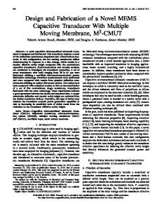
1. INTRODUCTION Micro Electro-Mechanical Systems (MEMS) are becoming essential to modern life. There are many applications of these devices in various areas of engineering (J.J. ALLEN, 2005). The present work aims to model, simulate and propose a process of manufacturing a MEMS electrostatic device called capacitive micromachined ultrasound transducer (CMUT). (B.T, KHURI-YAKUB, ET AL, 2000). CMUT technology emerged recently as an alternative to generate and receive acoustic signals. The acoustic signals have been used in several areas, such as in medical ultrasound analysis, in industrial instrumentation which uses ultrasonic sensors, in quality control for fault analysis, improve efficiency in electrical machines and many others (KINSLER, L. E., 1982). The main advantage of CMUT technology is the use of the same fabrication techniques used in microelectronics. Being the high points of the manufacturing techniques of microelectronics integrability, reduced in size, and large-scale production which creates a low cost final product. The basic structure of the CMUT can be seen in Figure 1a. With the application of electric voltage on the contacts electrical charges accumulate in the membrane over the substrate. This effect causing attractive forces between the two appears. If the applied voltage is alternating with a frequency f, force of attraction will vary causing the membrane to vibrate at a frequency determined by f (HALLIDAY, D.; RESNICK, R., 2003). The gap allows the membrane to vibrate freely thus generating acoustic waves (Figure 1b). conversely the CMUT can be used as a receiver of acoustic waves (figure 1c).
st
Proceedings of COBEM 2011 Copyright © 2011 by ABCM
21 Brazilian Congress of Mechanical Engineering October 24-28, 2011, Natal, RN, Brazil
(a)
(b)
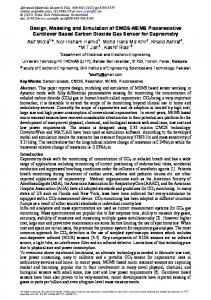
(c) Figure 1. (a) Representation of the physical structure of the CMUT. Note the empty space (cavity) bellow the membrane allowing complete vibration. The second driver is physically connected to the substrate. In (b) the process of sending the signal: applying an AC voltage on the plates (1) the membrane vibrates and generates sound waves (3). And finally (c) the process of sensing. the wave hits the membrane (1) causing its vibration (2), which changes the measured capacitance (3). A DC bias voltage can be applied to enhance the effect. This work consists basically of two main parts. The first is the modeling of CMUTs, involving the steps of analytical analysis and simulation using the finite element program ANSYS. This phase will show suitable dimensions for the devices. The second part of the proposed work focuses on manufacturing processes using two different materials: silicon and SU-8 (an epoxy-based photosensitive polymer).
2. MODELING Static simulations of CMUT's membranes subjected to atmospheric pressure serve as a basis for determining the value of the maximum deformation of the membrane. Membranes cannot deform too much in order to avoid its contact with the bottom electrode (below the cavity), what could cause a short circuit in the capacitor structure. Basically the important parameters for deformation of the membrane are: the geometry and material properties. The materials used as the membrane in the simulations are: the photoresist polymer (SU-8) (Chang, M., 2006) and silicon. Their mechanical properties can be viewed below (Table 1).
st
Proceedings of COBEM 2011 Copyright © 2011 by ABCM
Table 1: Mechanical Properties of SU-8 and Silicon. Material Young Poisson Modulus (E) () SU-8 4,2 GPa 0,220 Si 127GPa 0,278
21 Brazilian Congress of Mechanical Engineering October 24-28, 2011, Natal, RN, Brazil
Density (kg/m3) 1190 2330
First, we made an analytical analysis of how the membrane is deformed when it is subjected to a uniform load q (where q the atmospheric pressure). The results of this analysis can be seen in section 2.1. In section 2.2 we can see the computer simulation done by finite element method. 2.1. Analytical modeling Analytical analysis shows how the membrane is deformed when subjected to a uniform load q applied throughout the surface of one of its faces, as shown in Figure 2. Note that the geometry of the membrane is circular, its radius is a and its thickness is t.
Figure 2. Illustration of the load q (indicated by arrows) uniformly distributed on the membrane surface of circular radius a and thickness t. Load q is the atmospheric pressure. The textbook by Young and Budynas (2002) presents a suitable formula for the case of “bending of flat circular plate of constant thickness, with outer edge fixed and a uniform load over the entire plate on one face”. The following considerations apply: a membrane of a material with. Young´s modulus E and Poisson's ratio v, the membrane is flat, of uniform thickness, of homogeneous isotropic material, the thickness is at least four times smaller than the diameter, the maximum deflection is less than half the thickness, all forces are normal to the membrane, and the resulting stresses are lower than the elastic limit. The deflection of the membrane can be found by:
(1) Here r is the variable distance from the center of the membrane to its edge, y (r) is the deflection as a function of r, yc is the maximum deflection (found in the center of the membrane), Mc is the central bending moment, D is the rigidity Bending membrane. Equations (2), (3) and (4) below show how to obtain D, yc and Mc.
(2)
(3)
(4) The other parameters used are: membrane thickness t and the radius of the membrane a. With equation (1) one can plot the profile of deformation of the membrane. Through this profile, the point of maximum deflection is found. Figure 3 shows the profile for the two materials: silicon and SU-8. The profile was obtained by considering a thickness t = 3.5 m and a radius a = 50 m.
Proceedings of COBEM 2011 Copyright © 2011 by ABCM
st
21 Brazilian Congress of Mechanical Engineering October 24-28, 2011, Natal, RN, Brazil
Figure 3. The deformation of membranes for silicon and SU-8. The point of maximum deflection is highlighted, for silicon is 0.02011 m e to the SU-8 is 0.62750 m. These points are important in determining the thickness of the cavity of the CMUT. These results can be used as initial parameters for a more complexcomputational model (finite element method for example). Time spent with these analytical simulations is drastically reduced. 2.2. Computional Modeling The computational model was constructed using the commercial application for the finite element method Ansys (ANSYS 10.0, Ansys Inc., Canonsburg, PA.). The membranes are modeled three-dimensionally, which ensures a good precision in the results. A thin cylinder was constructed with diameter d (em µm) and thickness t (em µm) (figure 4a), and then the cylinder was discretized (figure 4b).
(a) (b) Figure 4. In (a) one can see the view of the cylinder. In (b) see if the same cylinder discretized. The basic element used for the formation of the membrane is a solid tetrahedral from ANSYS library: SOLID92. Figure 5 shows this element. After discretization, the movement of edge nodes is restricted in three directions, this is one of the boundary conditions.
st
Proceedings of COBEM 2011 Copyright © 2011 by ABCM
21 Brazilian Congress of Mechanical Engineering October 24-28, 2011, Natal, RN, Brazil
Figure 5. SOLID92 element belonging to the library of Ansys. This element is used as a basis to generate the cylinder representing the membrane of the CMUT. The letters (I, J, K, L, M, N, O, P, Q, R) represent nodes used to interconnect the various elements. The coordinate system is shown alongside. After defining and shaping the structure, static analysis were performed in order to obtain the deformation of the membrane with the application of atmospheric pressure and also with the application of both atmospheric pressure and DC voltage.
2.2.1. Static analyzes. The static analysis shows the effect of atmospheric pressure and also the effect of DC voltage on the deflection of the CMUT's membrane. Only circular membranes of silicon and SU-8 were considered. The mechanical properties of these materials can be seen in Table 1. The value of atmospheric pressure was considered 101.325KPa. Figure 6a (silicon) and figure 6b (SU-8) shows the results of static analysis only with the application of atmospheric pressure. These simulations were done considering the value of t = 3.5 m for the thickness and a diameter of d = 100m, same values considered for the analytic simulation. The results for deformation are: For the Silicon of 0.020211m for the SU-8 of 0.632244 m. As expected, deformation of the SU-8 is higher than that of Silicon, due to its lower modulus of elasticity.
(a)
(b)
Figure 6. Result of static simulation of the CMUT membrane made in the software Ansys considering only the application of atmospheric pressure. Figure (a) shows the result for silicon, the strain was approximately 0.020211m. In (b) shows the result for the SU-8, the deformation was about 0.632244 m. The values are negative because the reference used. Table 2 below compares the results from analytical model with the results from FEM. The small error shows that both models are consistent.
Proceedings of COBEM 2011 Copyright © 2011 by ABCM
st
21 Brazilian Congress of Mechanical Engineering October 24-28, 2011, Natal, RN, Brazil
Table 2. Maximum deformation of CMUT membranes of different materials. Membranes had thickness t= 3.5 m and diameter d = 100 m. Material Silicon SU-8
Maximum deformation from Analitical Model 0.02011 µm 0.62750 µm
Maximum deformations from FEM Model 0.02021 µm 0.63224 µm
Percentual error ≈ 0.5% ≈ 0.7%
Further analyzes take into account DC bias voltage as an extra load applied to the CMUT membrane. A practical reason to apply a DC bias is to approximate the top and bottom electrodes in order to enhance the capacitance or the electrostatic energy in each CMUT cell. The following analyzes consider both the atmospheric pressure and a DC bias voltage applied to the top electrode (membrane). Basically the parameters that affect the deformation of the membrane are: membrane thickness, membrane diameter, applied load (voltage and atmospheric pressure), the mechanical properties of materials making up the membrane. In the study below the value of atmospheric pressure was kept constant. Deformation curves were obtained as a function of voltage and membrane thickness. CMUT structure used as a model consists of a SU-8 or silicon circular plate with clamped edges, which also serves as the upper electrode of the capacitor, assembled on a highly doped silicon substrate that is also used as bottom electrode. The membrane and substrate are separated by an evacuated cavity (Figure 7). Ansys element TRANS126 is used to simulate the capacitive effect of the structure. This element is capacitive in nature and basically serves to convert electrostatic energy into mechanical energy or mechanical energy into electrostatic energy.
Figure 7. Model for the electrostatic simulations using Ansys element TRANS126. The DC voltage is applied in the model between the two nodes of a TRANS126 element, and Ansys software calculates the corresponding deformation (supposed unidirectional). The generation of TRANS126 elements is basically done as follows: First it is necessary to identify each node on the lower side of the previously meshed membrane (element SOLID92). Then, for each node of the membrane a new node must be generated immediately below it and at a distance corresponding to the capacitor gap. Finally, a TRANS126 element is generated with these two nodes (figure 7). Figures 8a and 8b show the results of the simulations for membranes with a diameter of 100 m made of silicon and SU-8, respectively. These simulations considered applied bias voltage in the range from 0V to 600V. The thicknesses of the membranes were 3.0 m, 3.5 m, and 4.0 m. SU-8 membranes showed a much higher dependency on the applied voltage when compared to Si membranes, as expected. This is due to the lower Young's Modulus of SU8.
st
Proceedings of COBEM 2011 Copyright © 2011 by ABCM
21 Brazilian Congress of Mechanical Engineering October 24-28, 2011, Natal, RN, Brazil
(a)
(b) Figure 8. Maximum deflection of the membranes as a function of the applied bias voltage: a) for silicon membrane, b) for SU-8 membrane. With these results it is possible to determine the dimensions that will be used in the manufacturing process. These values are summarized in Table 3. Table 3. Dimensional CMUT parameters determined through simulations Parameter Dimesion SU-8 Dimension Si Membrane Thickness (t) 3 – 4 µm ~ 3 µm Membrane diameter (d) ~ 100 µm ~ 100 µm Thickness gap cavity (g) 2 – 4 µm ~ 2 µm 3. FABRICATION PROCESS The majority of CMUTs studied nowadays use silicon technology in its fabrication. The membrane generally is fabricated by CVD (chemical vapor deposition) using a metal, polycrystalline silicon or silicon nitride or another dielectric covered with a conductor. Surface micromachining (Allen, 2005) is the most used technique for CMUTs, and several variations have been proposed (Buhrdorf et. al., 2003; Caronti et. al., 2006; Ergum; Yaralioglu; Khuri-Yakub, 2003; Kinight; Mclean; Degertekin, 2004). There is another method called wafer bonding, in which the device is fabricated in two parts in two distinct substrates. Then, in the final step, the two parts should be placed together and bonded (ERGUN et. al., 2005). In both methods the bottom electrode can be formed by a metallic film deposited or by doping silicon. Recently, CMUTs with membranes fabricated by with polymers (Chang; Deng, 2006) have been attracting much interest. These devices have a more flexible membrane, with better performance at frequencies in the range of several kilohertz. This work presents a fabrication route optimized for CMUTs with SU-8 membranes on glass substrates, instead of the traditional silicon technology. SU-8 is an epoxy-based negative photoresist, commonly used for MEMS. Samples of
st
Proceedings of COBEM 2011 Copyright © 2011 by ABCM
21 Brazilian Congress of Mechanical Engineering October 24-28, 2011, Natal, RN, Brazil
several sizes were fabricated in order to test the limits of fabrication process. CMUTs with circular and square shape membranes were obtained with the following sizes (lateral size in case of square membranes; diameter in case of circular membranes): 50 m, 100 m, 200 m, 350 m and 500 m. The thickness was around 5 m. 3.1. Manufacturing process for SU-8 CMUTs The manufacturing process proposed for the SU-8 is the bonding method where two pieces of structure are fabricated on separate substrates, being merged in the end (Carmen et. al, 2010). The process uses SU-8 bonding with SU-8, figure 9. Cavities and bottom electrodes are defined at the bottom part of the device in such a way that electrodes are arranged in groups (arrays). This is achieved by using a glass substrate covered with a thin layer of a metallic conductive film: the bottom electrodes pattern is etched in that film. Then, the whole structure is covered with a layer of SU-8 about 5 m thick. Finally, the cavities are etched in the SU-8 layer right on top of each electrode. SU-8's own developer was used as the etchant. Spin and bake processes were performed following the manufacturer recommendations for a 5 m coating (MicroChem, 2002). In parallel, the top part of the device includes the membrane structure prepared on another substrate. The membrane structure is composed of a layer of SU-8 about 4 m thick on an acetate substrate. However, between the substrate and the SU-8 membrane structure, it is deposited a sacrificial material to help release the substrate in the final step of the process. At this time, the positive photoresist AZ4620 is being tested as the sacrificial layer. Only the soft bake processes for each photoresist were carried out in this case in order to facilitate the release of the sacrificial layer.. As soon as both parts are finished, they must be immediately bonded applying some pressure at a temperature around 100°C for a period of time long enough to enhance the bonding, but short enough not to modify the properties of the sacrificial layer. Using a 0.5kg load for 5 minutes resulted in reasonably good CMUT samples.
(a)
(b)
(c)
(d)
(e)
(f)
Figure 10. Microfabrication process. The bottom part is shown from (a) to (c), while the top part is shown in (d). In (a) glass substrate and the conductive metallic layers deposited on it. In (b) the bottom electrode structure patter is achieved after lithography etching. (c) shows the SU-8 layer deposited on the bottom electrodes and etched to produce the cavities. (d) shows the membrane structure on acetate substrate. (e) shows the bonding. (f) shows the final CMUT structure.
3.2. Results of fabrication process Figure 10 shows some CMUT structures fabricated with SU-8. Figure 10(a) shows the bottom part, before the bonding process, with the cavities already etched within the SU-8 layer on top of the circular electrodes. Figure 10(b) shows final circular CMUT structures after completing the bonding process. Figure 10(c) shows square shape CMUTs. Finally, figure 10(d) shows some types of faults observed in some membranes, which probably occurred during the release of the sacrificial layer.
Proceedings of COBEM 2011 Copyright © 2011 by ABCM
st
21 Brazilian Congress of Mechanical Engineering October 24-28, 2011, Natal, RN, Brazil
(a)
(b)
(c)
(d)
Figure 10. CMUT structures fabricated using the bonding process. (a) Structure of the base for some CMUT with diameter of 200m. (b) Test sample with circular membranes of 50m after the bonding process . (c) square membranes of 200m after the bonding process . (d) CMUT wit membranes of 500 m bonded to base
5. CONCLUSIONS This work presented a very useful design methodology for capacitive micromachined ultrasound transducers. It includes a simple and fast analytical method using common formulas available in textbooks and suitable for initial assumptions. Using such first results as a starting point, more complex computer simulations can be carried out based on the “Finite Element Method”. Such simulations are very useful to design CMUT devices that fulfill certain applications. Such methodology was applied for the design of CMUTs based on silicon and on SU-8. Particularly, this group is interested in mastering SU-8 based CMUTs for applications in the range of tenths to hundreds of kilohertz. A fabrication process based on the bonding of two SU-8 parts was successfully demonstrated in this article for the first time. Such process is relatively inexpensive, but requires strict control since several parameters affect the bonding: temperature, pressures, SU-8 conditions (bake, exposure to ultra-violet light, thickness), etc. Therefore, a great effort will be spent on optimizing this process for use in mass production. Electrical tests will be performed in future in order to evaluate operating conditions of the device like vibration operations and real electrical voltage values. CMUT have showed to have potential to be a good device to emit and receive sound waves in different frequency ranges and replace the piezoelectric devices in some applications. 7. ACKNOWLEDGEMENTS The authors are grateful to Microfabrication Laboratory of the Brazilian Synchrotron Light Laboratory (LNLS); Laboratory of Integrated Systems of Polytechnic School (LSI-EPUSP) and CNPq.
Proceedings of COBEM 2011 Copyright © 2011 by ABCM
st
21 Brazilian Congress of Mechanical Engineering October 24-28, 2011, Natal, RN, Brazil
8. REFERENCES Allen, J.J., 2005, “Micro electro mechanical system design”, CRC Press. BUHRD0RF A. et. al., 2003 “Fabrication and Characterization of a New Capacitive Micromachined Ultrasonic Transducer (CMUT) Using Polysilicon as Membrane and Sacrificial Material”. 2003 IEEE Ultrasonics Symposium, p. 1951-1954. Carmen A., Perdigones F., Moreno, J. M., and Quero, J. M., 2010, BETTS: bonding, exposing and transferring technique in SU-8 for microsystems fabrication, J. Micromech. Microeng. 20 035008 (7pp). CARONTI, A.; CALIANO, G.; CAROTENUTO, R.; SAVOIA, A.; PAPALARDO M.; CIANI, E.; FOGLIETTI, V. , 2006. “Capacitive micromachined ultrasonic transducer (CMUT) arrays for medical imaging”. Microelectonics Journal, v. 37, p. 770-777. Chang, M. M-W.; Deng, M. T-M., 2006, “Polimer-based Capacitive Micromachined Ultrasonic Transducers (CMUT) for Micro Surgical Imagim Applications”. Porceedings of the 1st IEEE International Conference on Nano/Micro Enginnered and Molecular Systems, p. 61-65. Chen, et. al., 2008. “A Capacitive Micromachined Ultrasonic Transducer Array for Minimally Invasive Medical Diagnosis”. Journal of Microelectromechanical systems, p. 599-610. v. 17. Chiou, D. et. al., 2007. “Characterization Optimization Dsign of the Polymer-Based Capacitive Micro-Arreyed Ultrasonic Transducer”. Japanese journal of Applied Physics. Vo. 46 pp. 7496-7503. 2007. ERGUM, A. S.; YARALIOGLU, G. G.; KHURI-YAKUB, B., 2003. Capacitive Micromachined Ultrasonic Transucers: Theory and Technology. Journal of Aerospace engeneering, April, p76-84. Ergun, A. S. et, al. 2005, “Capaicitive Micromachined Ultrasonic Transducers: Fabrication Technology” IEEE Trans. Ultrason., Freq. Contr., v. 52, p. 2242-2258. Halliday D.; Resnick, R., 2003, “Fundamentos de Física III”. 5ed.,Livros Técnicos e Científicos, Brasil. Jiguet, S. et. al., 2005. “Conductive SU8 Photoresist for Microfabrication”. Adv. Funct. Mater. V15, p. 1511-1516 KINIGHT, J.; MCLEAN, J.; DEGERTEKIN, L., 2004. “Low Temperature Fabrication of Immersion Capacitive Micromachined Ultrasonic Transducers on Silicon and Dielectric Substrates”. IEEE Trans. Ultrason., Freq. Contr., v. 51, p. 1324-1333. Kinsler, L. E., et. Al.,1982, “Fundamentals of Acoustics”, John Wiley & Sons. Khuri-Yakub, B.T., Cheng, C.H., Degertekin, F.L., Ergun, A.S., Hansen, S.T., Jin, X.C., Oralkan, O., 2000 “Silicon micromachined ultrasonic transducers”, Jpn. J. Appl. Phys., vol. 39, pp. 2883 - 2887. Madou, M. J., 2002, “Fundamentals of Microfabrication the Science of Miniaturization”. CRCPress, USA. MicroChem, 2002, “NANO SU-8 Negative Tone Photoresist Formulations 2-25”, Micro Chem, USA, 14 March 2011, Sheng Li, et. al., 2003, “Fabrication of micronozzles using low-temperature wafer-level bonding with SU-8”, J. Micromech. Microeng. 13 (732–738). Young, W. C.; Budynas, R. G.,2002, “Roark's Formulas for Stress and Strain”. McGraw-Hill, USA, 2002.
9. RESPONSIBILITY NOTICE The authors are the only responsible for the printed material included in this paper.