MPA14-9 Design Methodology of Multiple-Valued Logic Voltage-Mode
Recommend Documents
AbstractâIn this paper we propose a new digital system design methodology which ... and VerilogHDL for FPGA implementation. ... other will convert the NSL to SystemC or VerilogHDL or VHDL. ... It says, âThe components may be of digital,.
MP4. MP3. MP2. MP5. MP6. MP0. MP7. Fig. 2. Modular behavioural specification by means of Petri nets. To obtain the economical implementation and easy ...
In the sequel, a detailed presentation of those advantages ... the advantages of the fuzzy logic controllers (FLC), that is ... calculus or first-order predicate logic.
Logic circuits perform operation on digital signal. • Digital signal: signal values
are restricted to a few discrete values. • Binary logic circuits: signals can have two
...
This thesis presents a systematic approach to füzzy-logic modeling and control ...
In the proposed methodology, the füzzy mode1 of the system and control rules ...
science. The last section concludes with some suggestions about the art and practice of system design. 1. While âsystem designâ in this paper refers primarily to ...
Proposed work describes methodology, content development and implementation of hardware based training on complex programmable logic devices (CPLD) ...
MOTIVATION. Digital signal processing, traditionally the domain of Government ... multirate signal processing applications. Asynchronous ... Applications to multirate signals process- ... Note, however, that vectors and arrays have always been.
Methodisch ontwerpen : ontwerpmethoden, voorbeelden ... Denken en doen bij experimenteel onderzoek : een inleiding tot het begrijpen en zelf verrichten van ...
electrical contractors, wanted to show their design and engineering capabilities. It had to be innovative and so they decided to design an office building with a flexible construction and notable use of .... Each layer represents an abstraction of th
CHAPTER 3. RESEARCH ... Study Description: Sample Population. The study ...
The third part included a comparison of computer exam scores to paper and.
considering the limitations of teaching hardware along with necessary ... board along with necessary electronic devices, components and laboratory tools; ...
applications of linear differential equations in engineering problems –Electrical
Circuits, Mechanical .... solutions, pH measurement, Polarisation, Overvoltage. ...
John E. McMurry and Robert C. Fay, Chemistry, 5th Edition, Pearson, 2008. 3.
Introduction ...... (even) parity for a 3-bit message. Three-Bit Message. Odd Parity
Bit. Even Parity Bit. X. Y. Z. P. P ... 0 nul 16 dle 32 sp 48 0 64 @ 80 P 96 ` 112 p.
marketing; they form together the provisions for good service performance [15, .... or in a luxury restaurant, the purch
Xfuzzy is free software; you can redistribute it and/or modify it under the terms of the GNU. General Public .... 4*a*(1-a) defuzzification, defuz defuzzification center of area ...... The bindkey used to introduce a new module (a call to a rule base
Digital Logic Design. Chapter 1. Introduction. Fall 2011. CSE3201. 2. Introduction
. • This course is about Design Techniques for. Digital System, a more exact ...
89. 6. BOOLEAN LOGIC DESIGN. 6.1 INTRODUCTION. The process of
converting control objectives into a ladder logic program requires structured
thought.
Number System, Digital Design Fundamentals, Understand and Design
Functions of Combinational ... Floyd T. L., Digital Fundamentals, 10th edition,
Pearson ... Mano M. M, Kime C. R , Logic and computer design fundamentals,
2nd edition.
To learn how to analyze a given digital logic circuit by finding the Boolean ... Now after drawing the circuit above, we find that its truth table is as shown below ...
Digital Design: Principles and Practices, Wakerly,. Prentice Hall. • Advanced
Digital Design with the Verilog HDL, M. Ciletti, Prentice hall. • Contemporary
Logic.
□C. H. Roth, Jr. Fundamentals of Logic. Design, 7th edition, Cengage Learning,.
2013. 4. Schedule. □ 9/12. §1 Introduction, Number Systems and Conversion.
24. Draw the Q output of each flip-flop, if they are initially RESET. .... How many flip-flops are required to divide a frequency by thirty-two? 5 Flip-flops. 1 kHz.
MPA14-9 Design Methodology of Multiple-Valued Logic Voltage-Mode
of MOS transistor and can function with only one control signal. (usually a clock), i.e., its complementary form is not needed. Exploiting the latter useful feature, one can design MVL data ... cascade inverter circuits, with their source and ground voltages connected ... voltage, y, of the node x reduces to the voltage 3-VTH volts,.
DESIGN METHODOLOGY OF MULTIPLE-VALUED LOGIC VOLTAGE-MODE STORAGE CIRCUITS I. Thoidis, D. Soudris, I. Karafyllidis, A. Thanailakis, T. Stouraitis* Laboratory of Electrical and Electronic Materials Technology Dept. of Electrical and Computer Eng. Democritus University of Thrace 671 00 Xanthi, Greece, [email protected] *VLSI Design Lab, Dept. of Electrical and Computer Eng. University of Patras, 26110, Patras, Greece
ABSTRACT A novel methodology designing for Multiple-Valued Logic voltage-mode storage circuits is introduced. Using the proposed inverter-based unit, uni-signal controlled pass gates and True Single-Phase Clocked Logic-based output units, efficient r-ary (where r is the radix) dynamic and pseudo-static latches can be designed. They exhibit regular, modular, and iterative structure, which means that the for Multiple-Valued Logic circuits are VLSI implementable. Also, These circuits use two kinds of MOS transistors, i.e., enhancement and depletion mode. Since we use only clock signal, additional contribution to low power dissipation of the derived circuits is been made. Comparisons with existing circuits prove substantial improvements in terms of speed, power consumption, and transistor count.
1.
Comparing the quaternary pseudo-static produced by the proposed methodology with an existing circuit [11], it is concluded that the former circuit exhibits substantially-improved features.
2.
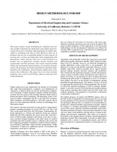
THE DESIGN METHODOLOGY
Applying the proposed methodology r-ary latches, where r is the radix, can be designed. Their general structures are shown in Fig. 1. They consist of three basic building blocks, namely the inverter-based unit (level-corrector), the uni-signal controlled pass gate, and the TSPCL-based output unit. The main features of these building blocks are presented in the next paragraphs. It should be noted that, both enhancement and depletion transistors are used [12].
INTRODUCTION
Multiple-Valued Logic (MVL) circuits have been attracting researchers in recent years, the reason arises from the fact that some critical features related to the reduction of the number of the interconnections and the increased information content per unit area [1-3]. Two kinds of MVL circuits based on MOS technology have been developed, namely the current-mode MVL circuits [4] and the voltage-mode MVL circuits [5-8, 10, 12]. In this paper, a methodology for designing MVL voltage-mode dynamic and pseudo-static latches is presented. Efficient new building blocks, namely, inverter-based unit (level-corrector), the uni-signal controlled pass gate, and the True Single-Phase Clocked Logic (TSPCL)-based output unit, for r-ary logic implementations, are introduced. Combining the first circuit with the TSPCL-based output unit or the uni-signal controlled pass gates, which are also introduced, an r-ary latch can be designed. As an application, the implementation of the above MVL latches in quaternary logic (r=4) is provided. The proposed MVL circuits are characterized by two threshold voltages for each type of MOS transistor and can function with only one control signal (usually a clock), i.e., its complementary form is not needed. Exploiting the latter useful feature, one can design MVL data paths similar to the True Single-Phase Clocked Logic (TSPCL) [9] approach of the binary logic, which avoids race condition problems. Also, the existence of TSPCL design style results into MVL circuits with low power consumption.
INVERTERBASED UNIT
x
TSPCL-BASED OUTPUT UNIT
(a)
z
clock
Uni-signal controlled pass gate x
INVERTER-BASED UNIT
clock (b)
z
Uni-signal controlled pass gate
Figure 1. The structure of MVL latches, (a) dynamic and (b) pseudo-static.
0-7803-4455-3/98/$10.00 (c) 1998 IEEE
2.1
Inverter-based unit
m
The inverter-based unit performs voltage level correction, i.e., it produces the exact logic level voltage, when the input voltage value has small difference from the precise voltage value of the associated logic level. For a given radix r, the proposed inverter-base unit (levelcorrector) has the structure shown in Fig. 2. It comprises two aary Logic Level-Correction Module (aLLCM), where 0