NCL+: Return-to-One Null Convention Logic Matheus T. Moreira, Carlos H. M. Oliveira, Ricardo C. Porto, Ney L. V. Calazans Pontifical Catholic University of Rio Grande do Sul GAPH – Faculty of Informatics Porto Alegre, Brazil {matheus.moreira, carlos.oliveira, ricardo.porto}@acad.pucrs.br,
[email protected] As far as the authors could verify, this is the first work to propose the design and evaluate the performance of NCL gates assuming the RTO protocol. Albeit other works like references [7]-[10] discuss alternative implementations of NCL gates, all previous proposals rely on the assumption of an RTZ handshake protocol. In this way, this work stands off by proposing a novel design style for asynchronous circuits, which enables more power efficient designs and better design space exploration, while maintaining delay insensitive and the support for standard-cell-based design.
Abstract— Asynchronous paradigms are a way to deal with hard problems in newer technologies. Among the templates for ensuring efficient asynchronous design, Null Convention Logic (NCL) appears as a fast and relatively low area and power option, enabling semi-custom design. This work proposes a new asynchronous logic template, NCL+, which is a modification of NCL to support the return-to-one protocol. A basic library of NCL+ standard-cells, with different driving strengths enables comparison between NCL and NCL+. While no significant differences in area arise, results suggest that a trade-off of power versus forward propagation delay exists. Accordingly, NCL+ provides more power efficiency and NCL provides smaller forward propagation delays.
I.
II.
The asynchronous paradigm is, in fact, a class that encompasses several possible design templates. Each template can employ a distinct combination of delay model, data encoding and handshake protocol [2] [3] [4] [11]. Furthermore, each may require different components to be implemented in silicon. Yet, often used templates employ the QDI design style using an m-of-n DI code coupled to the 4-phase handshake protocol. One of the reasons behind the adoption of these templates is the fact that they allow simple timing closure and analysis, while maintaining the robustness inherent to QDI [11]. Also, due to the 4-phase protocol, completion can be easily computed and logic/arithmetic blocks are easier to implement than with 2-phase protocols, which reduces design complexity and hardware overhead [2].
INTRODUCTION
As process variations get critical and integration scales evolve to billions of transistors in a single chip, timing closure of high complexity synchronous integrated circuits (ICs) becomes an increasingly complex task [1]. Thus, asynchronous design techniques receive growing attention from the VLSI community. Currently, the most used circuit delay model for asynchronous design is the quasi-delayinsensitive (QDI) [2], because it allows simpler timing closure and analysis and can be implemented using standardcell based approaches. Also, according to Martin [2], to design QDI circuits, 1-of-n delay insensitive (DI) codes [3] coupled to a 4-phase handshake protocol [4] are mostly used, due to their high power/area/speed efficiency and reduced complexity. For such circuits, different templates support building sequential/combinational logic. Among these, the null convention logic (NCL) [5] enables power-, area- and speed-efficient standard-cell-based design.
There are many ways to encode data in a DI manner. Even though new codes (see e.g. [11]) are often suggested for specific applications, the m-of-n class of codes and specifically 1-of-n codes, are widespread in VLSI design [2]. A key factor for the success of 1-of-n data codes is the fact that in such codes data validity tests are simple and completion circuits require little hardware when compared to other DI codes. In 1-of-n codes, data is represented using n wires. Data validity is identified when exactly one of the n wires is at a given logic value and data absence can be marked by any of the 2n-n other code words. The data absence code word is called spacer, as it always separates two successive 1-of-n codes in a data channel. Classically, the return-tozero (RTZ) protocol is used, where the spacer is a code word formed by n zeroes and valid code words are all those with exactly a single wire at logic ‘1’.
NCL gates assume the use of return-to-zero (RTZ) handshake protocols [5]. However, recent findings of the authors demonstrated the potentials of using the return-to-one (RTO) protocol for other QDI templates [6]. This paper proposes and evaluates NCL+, a modification of NCL where gates assume the use of the RTO protocol. Doing so, the unavoidable series of n transistors in the pull-up network of an NCL gate, where n is the number of inputs, is moved to the pull-down network, classically preferred for its higher electron mobility. A set of 70 NCL+ gates employing 14 different functionalities, each with 5 different driving strengths, was designed to layout level and compared in a practical design to a previously designed equivalent set of NCL gates. Electrical simulation results point to a tradeoff of power versus forward propagation delay, where NCL+ provides better power efficiency and NCL presents lower propagation delay figures.
978-1-4799-0066-4/13/$31.00 ©2013 IEEE
THE RETURN-TO-ONE PROTOCOL
Figure 1(a) depicts the 1-of-2 code RTZ conventions, which use two wires, called D.t and D.f, to represent a single bit of information, a '0' bit is denoted by D.f at logic ‘1’ and a '1' bit by D.t at logic ‘1’. In 1-of-n RTZ conventions, any code word with more than one wire at 1 cannot represent valid data.
836
Wire Name Spacer Bit '0' Bit '1' Wire Name Spacer Bit '0' Bit '1' 1 1 0 D.t 0 0 1 D.t 1 0 1 D.f 0 1 0 D.f (a) (b) Figure 1 – 4-phase 1-of-2 data encoding for (a) RTZ, (b) RTO protocols.
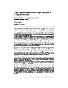
Figure 3 – Symbol of an NCL gate.
In a system using the RTZ protocol, data transmission occurs as Figure 2(a) depicts. Communication starts with all wires at logic ‘0’ (the all-0s spacer). Next, the sender puts data in the channel (D.f, D.t), which is acknowledged by the receiver with the ack signal. After the sender receives ack, it produces a spacer to end communication. The receiver then lowers ack, after which another communication can take place.
In NCL gates, the output will switch to logic ‘0’ when all N inputs are at logic ‘0’ and to logic ‘1’ when at least M of its N inputs are at logic ‘1’. Otherwise, it keeps its output state. There are different ways to design NCL gates in CMOS, such as the six approaches that Parsan and Smith discuss in [9]. Among these, classical static implementations are of particular interest, as they are simpler and constitute a good area and power compromise. Accordingly, this work assumes the use of static implementations of NCL gates. In NCL+, gates also implement a threshold function, a subset of which appears in Figure 4, where M is the defined gate threshold (written inside each gate). However, the assumption of the RTO protocol mandates the switching function of an NCL+ gate to be the reverse of its NCL counterpart: the output will only switch to logic ‘1’ when all inputs are at logic ‘1’ and will only switch to logic ‘0’ when at least M of its inputs is at logic ‘0’. For other combinations of inputs, the output keeps the previous value. Figure 5(a) shows the CMOS schematic of a 3-input, M=2 NCL threshold gate, and Figure 5(b) shows the schematic of an equivalent NCL+ gate. Note that the gate drawn with dotted lines in Figure 4 is the 2-of-3 gate described in Figure 5.
(a) (b) Figure 2 – Example of 4-phase (a) RTZ and (b) RTO 1-of-2 data transmission, where sp stands for the spacer.
The RTO protocol, described in [6] is similar to RTZ. The only difference is that data wire values are reversed. Figure 1(b) shows the conventions for the 1-of-2 RTO protocol. A spacer is represented by n wires at 1 (all-1s). Here, a '1' bit is given by D.t at logic ‘0’ and a '0' bit by D.f at logic ‘0’. As Figure 2 (b) shows, differently from RTZ, RTO data transmission starts after the all-1s value is in the data channel. As soon as the sender puts valid data in the channel (D.f, D.t) the receiver may acknowledge it, by lowering ack. Next, all data wires must return to logic ‘1’ to denote a spacer, which ends the transmission. When the receiver detects a spacer, it raises ack and new data can follow. The idea behind the RTO protocol is very simple, and albeit a 1-of-2 example is used here, any m-of-n code can support both protocols. Also, an RTO-RTZ domain interface for a same m-of-n code requires only n inverters. As a generalization for m-of-n codes, an RTO-based D.x wire logic value can be translated from RTZ by Equation (1): {x ∈ Ν | 0 ≤ x ≤ m − 1} , RTO ( D.x) = ¬RTZ ( D.x )
Figure 4 - Basic set of 14 NCL+ gates.
(1)
where expressions RTO(D.x) and RTZ(D.x) correspond to the wire logic values in the RTO and RTZ domains, respectively. In this way, according to Martin [12], the conversion of data from one domain to another is DI. III.
NCL+
In NCL design, basic components are sometimes called threshold gates, but this is imprecise. In fact, NCL gates couple a threshold 1 function [13] with positive integer weights assigned to inputs to the use of a hysteresis mechanism. This supports DI circuit design using dual rail or 1-of-4 data encoding [5]. Figure 3 shows the NCL gate symbol: N is the number of inputs, and M is the gate threshold.
Figure 5 – Transistor topology for the 3-input M=2 threshold gate in NCL (a) and NCL+ (b).
Authors designed a set of 70 NCL+ threshold gates at the layout level as standard-cells in the STMicroelectronics 65nm technology, according to the flow proposed in [14]. The fourteen distinct threshold functions described in Figure 4 were designed, each being implemented in five different
1
The authors reinforce that this use of the term threshold has no relationship with the term threshold applied to define the voltage at which a transistor starts switching.
837
driving strengths: X2, X4, X7, X9 and X18. This set effectively supports a wide variety of functionalities. Note that the shadowed gates, where the threshold is the same as the number of inputs. These have exactly the same implementation in either NCL or NCL+, as the threshold for the output to switch to logic ‘1’ or to logic ‘0’ is the same. In terms of standard-cell area, NCL and NCL+ are typically equivalent, because they require the same number of transistors and have similar topology. IV.
digital and analog parts were Cadence Incisive and Spectre, respectively. Simulation scenarios assumed typical fabrication process and typical operating conditions (25o C and 1 Volt). Also, the adder inputs slope was fixed at 50ps and output loads varied depending on the cells´ driving strength, to obtain a load equivalent to FO4 in the last full-adder and in the S outputs as well. The SystemC verification block consists of a random data generator that feeds the adder inputs, and a data checker that verifies its correct behaviour. Also, this block measures average, best and worst case delays to perform the sum of two values for forward delay and transmission delay, as well as the module throughput, measured in millions of operations per second (MOPS). Precise dynamic and idle power values were measured using the analog simulator. The former is given as the average power of the adder when operating, while the latter is the average power when idle (quiescent and filled with spacer data, i.e. all-0s for NCL and all1s for NCL+). As dual-rail data values are always balanced for both logic values '1' and '0', random data can be used without compromising the generality of the obtained results.
NCL VERSUS NCL+
To compare the NCL and NCL+ templates a 32-bit ripple carry adder described in SPICE, corresponding to the block diagram of Figure 6(a) was used. The circuit writes the sum of X and Y to the S output and produces carry signal C. The internal carry signals are represented by Ci. For simplicity the adder assumes the use of dual-rail (or 1-of-2) encoding. Thus, each data bit takes two wires, false (f) and true (t). Figure 6(b) and Figure 6(c) describe the NCL+ gate level implementation of the blocks that compose the circuit. Five versions of the adder exist, one for each of the driving strengths.
TABLE I summarizes the measured values for throughput (MOPS), forward propagation delay (fwd. delay), total computation delay (tot. delay), dynamic power (dyn. pwr.) and idle power (idle pwr.). Area results are omitted, because the observed areas for the same driving strength circuits are always equivalent.
(a)
TABLE I – Simulation results for NCL and NCL+ adders.
(b) (c) Figure 6 –32-bit ripple carry adder: (a) block diagram; gate level schematics of the NCL+ (b) half adder and (c) full adder.
For comparison, the adder was also implemented using the NCL template for the same five driving strengths. Previously designed NCL gates [15] were employed. The gate level schematics for the NCL implementations are the same as those of NCL+ in Figure 6(a) and (b), where NCL+ gates are replaced by NCL gates of the same threshold. The choice for this case study circuit is due to the fact that it employs a series connection of a half adder to a series of 31 full adders, resulting in long gate level combinational paths. This is a good case study for evaluating the efficiency of threshold gates in each template in terms of delay and power. Also, it provides a fixed fan-out of 4 (FO4) for gates that generate internal carry signals, avoiding unrealistic power and timing analysis.
MOPS fwd. delay (ps) tot. delay (ps) dyn. pwr (mW) idle pwr. (µW)
X2 536 564 1866 0.370 2.785
X4 622 485 1608 0.530 3.898
NCL X7 691 444 1446 0.845 6.032
X9 694 488 1440 1.164 8.002
X18 835 424 1197 1.748 10.343
MOPS fwd. delay (ps) tot. delay (ps) dyn. pwr (mW) idle pwr. (µW)
X2 600 692 1668 0.409 2.245
X4 657 673 1521 0.549 3.131
NCL+ X7 673 602 1484 0.711 4.069
X9 744 549 1344 0.901 5.159
X18 820 473 1219 1.745 9.587
As TABLE I shows, circuits with similar driving strength have similar MOPS. However some of them present considerable deviations, like X2, for instance, which presents almost 12% higher MOPS for NCL+. These deviations are due to parasitic and gate capacitance effects, given that the delay of the standard-cells depends not only on its driving strength but also on factors such as input slope and output load, which are directly related to these effects. Also, deviations were expected, given the differences in NCL and NCL+ gate design processes.
To scrutinize the effects of each design style, a mixedsignal simulation environment was set up for each of the 10 adders. It consists of a VHDL testbench that instantiates an adder described in SPICE and a verification block, described in SystemC. A VHDL-AMS description was used for converting analog to digital signals and vice-versa. All SPICE descriptions employed post-layout extracted gates, in order to account for parasitics. The employed simulators for
Figure 7 gives another perspective on the results. First, Figure 7(a) presents the average energy consumption per operation for each NCL and NCL+ design. These results were obtained from the measured dynamic power and MOPS of each design. Similarly, Figure 7(b) presents the
838
results for idle power and Figure 7(c) the percentage of forward propagation delay in total delay. Note that only the intersection between similar MOPS intervals appears in the graphs.
V.
CONCLUSION
This paper proposes a new asynchronous design template, named NCL+, which furnishes an alternative to NCL. It provides a new trade-off of power and forward propagation delay. The area occupied by equivalent circuits in both templates is roughly the same. Accordingly, the proposed template is promising for coping with power requirements in current and future technologies. In this way, NCL+ enables a new approach for asynchronous design, providing better design space exploration capability.
(a)
Finally, reducing idle power and increasing energy efficiency is of great importance for contemporary challenges like battery-based systems low power budgets and green computing challenges. Asynchronous techniques are already an appealing solution for such challenges. In this context, the proposed NCL+ can lead to further improvements for these techniques. ACKNOWLEDGEMENTS This work is partially supported by the CAPESPROSUP (under grant 11/0455-5). Ney Calazans acknowledges CNPq support under grant 310864/2011-9. Authors acknowledge support granted by the INCT-SEC, process no. 573963/2008-8.
(b)
REFERENCES [1] [2]
[3] [4] (c)
[5]
[6]
Figure 7 – Energy, power and delay comparison between NCL and NCL+: (a) energy consumption per operation; (b) idle power; (c) percentage of the total delay represented by forward propagation delay.
[7]
The obtained results suggest that NCL+ is more energy efficient when compared to NCL. As Figure 7(a) shows, its energy consumption per operation is typically lower for equivalent MOPS designs. Also, as Figure 7(b) shows, the total idle power is lower in all cases, presenting significant savings and suggesting lower leakage currents at the standard-cell level for NCL+. This is particularly interesting for asynchronous designs, as some parts of these circuits are usually quiescent while others are operating. In this way, NCL+ potentially leads to systematic total power savings. However, for forward propagation delay, results show that NCL+ presents worse results in all cases. In this way, the obtained results point to a power and forward propagation delay trade-off for NCL and NCL+.
[8] [9] [10] [11]
[12] [13]
[14]
[15]
839
ITRS, “Design Section”, 2011, available at http://www.itrs.net. A. J. Martin and M. Nyström. Asynchronous Techniques for Systemon-Chip Design. Proceedings of the IEEE, June 2006, 94(6), pp. 1089-1020. T. Verhoeff. “Delay-insensitive codes- an overview”. Distributed Computing, 3(1), 1988, pp. 1-8. P. Beerel, R. Ozdag M. Ferretti. “A Designer’s Guide to Asynchronous VLSI”. Cambridge University Press, 2010, 337 p. K. M. Fant, S. A. Brandt. “NULL convention logic: a complete and consistent logic for asynchronous digital circuit synthesis”. In ASAP’96, 1996, pp. 261-273.
M. Moreira, R. Guazzelli and N. Calazans, “Return-to-One Protocol for Reducing Static Power in C-elements of QDI Circuits Employing m-of-n Codes”. In: SBCCI’12, Brasilia, Brazil, 2012. 6 p. L. Zhou. “Bit-Wise MTNCL: An ultra-low power bit-wise pipelined asynchronous circuit design methodology”. In: MWSCAS’10, 2010, pp. 217-220. S. Yancey, S. C. Smith. “A differential design for C-elements and NCL gates”. In: MWSCAS’10, 2010, pp. 632-635. F. A. Parsan and S. C. Smith. “CMOS implementation comparison of NCL gates”. In: MWSCAS’12, 2012, pp. 394-397. J. F. Pons. “State-holding free NULL Convention LogicTM”. In: MWSCAS’12, 2012, pp. 322-325. W. J. Bainbridge, W. B. Toms, D. A. Edwards, and S. B. Furber. “Delay-insensitive, point-to-point interconnect using m-of-n codes”. In: ASYNC´03, 2003, pp. 132- 140. A. J. Martin. “The limitations to delay-insensitivity in asynchronous circuits”. In: AUSCRYPT’90, 1990, pp. 263-278. S. L. Hurst. “An Introduction to Threshold Logic: A Survey of Present Theory and Practice”. The Radio and Electronic Engineer, 37(6), June 1969, pp. 339-351. M. Moreira, B. Oliveira, J. Pontes, N. Calazans. “A 65nm Standard Cell Set and Flow Dedicated to Automated Asynchronous Circuits Design”. In: SOCC’11, 2011, pp. 99-104. M. Moreira, C. Oliveira, R. Porto and N. Calazans. “Design of NCL Gates with the ASCEnD Flow”. In LASCAS’13, 2013, 4p.